Structures of Fluorinated Graphenes and Their Signatures
Abstract
Recent synthesis of fluorinated graphene introduced interesting stable derivatives of graphene. In particular, fluorographene (CF), namely fully fluorinated chair conformation, is found to display crucial features, such as high mechanical strength, charged surfaces, local magnetic moments due to vacancy defects and a wide band gap rapidly reducing with uniform strain. These properties, as well as structural parameters and electronic densities of states are found to scale with fluorine coverage. However, most of the experimental data reported to date neither for CF, nor for other CnF structures complies with the results obtained from first-principles calculations. In this study, we attempt to clarify the sources of disagreements.
pacs:
73.22.Pr, 63.22.Rc, 61.48.Gh, 71.20.-bI Introduction
Active research on graphenenovo1 revealed not only numerous exceptional properties geim ; berger ; kats ; hasan2010 but also have prepared a ground for the discovery of several graphene based materials. Preparation of freestanding graphene sheets with nonuniform oxygen coverage have been achieved.dikin More recently the synthesis of two-dimensional hydrocarbon in honeycomb structure, so called graphane novo-graphane (CH), showing diverse electronic, magnetic and mechanical properties sofo ; boukhvalov ; graphane-h1 ; graphane-h2 ; graphane-m is reported.
According to Pauling scale F has electronegativity of 3.98, which is higher than those of C(2.55), H(2.20) and O(3.44), and hence fluorination of graphene is expected to result in a material, which may be even more interesting than both graphene oxide and CH. Before the first synthesis of graphene, fluorinated graphite has been treated theoretically. charlier ; takagi Owing to promising properties revealed for CH, fluorinated graphene structures are now attracting considerable interest boukhvalov2 ; cheng ; robinson ; nair ; yeni1 ; yeni2 ; yeni3 ; yeni4 despite uncertainties in their chemical compositions and atomic structures. In an effort to identify the structures of fluorinated samples, previous theoretical models attempted to deduce the lowest energy structures. charlier ; boukhvalov2 In addition, band gaps of different structures calculated within Density Functional Theory (DFT) are compared with the values revealed through specific measurements.robinson ; nair However, neither the stability of proposed structures are questioned, nor underestimation of band gaps within DFT has been a subject matter. Raman spectrum by itself, has been limited in specifying CnF structures.nair
In this work, we first determined stable CnF structures for . Then we revealed specific properties (such as internal structural parameters, elastic constants, formation and binding energies, energy band gap and photoelectric threshold) for those stable structures as signatures to identify the derivatives probed experimentally. We placed an emphasis on fully fluorinated graphene or fluorographene (CF), in which D and G Raman peaks of bare graphene disappear after long fluorination period.robinson ; nair Present study reveals that the properties, such as structural parameters, binding energy, band gap and phonon modes of various fluorinated structures are strongly dependent on the binding structure of F atoms and their composition. Some of these properties are found to roughly scale with F coverage. While the stable C2F chair structure is metallic, CF is a nonmagnetic insulator with a band gap, , being much larger than 3 eV, i.e. a value attributed experimentally to fully fluorinated graphene. In view of the calculated diffusion constant, Raman active modes and other properties, available experimental data suggest that domains (or grains) of various CnF structures with extended and imperfect grain boundaries can coexist after fluorination process. Hence the measured properties are averaged from diverse perfect and imperfect regions.
II Computational Methodology
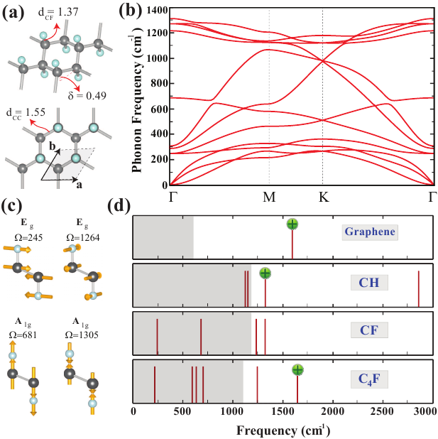
Our predictions are obtained from first-principles plane wave calculationsvasp within DFT, which is demonstrated to yield rather accurate results for carbon based materials. Calculations are performed using spin-polarized local density approximation (LDA)lda and projector augmented wave (PAW) potentials.paw Kinetic energy cutoff for plane-wave basis set is taken as 500 eV. In the self-consistent potential and total energy calculations of fluorographene a set of (25x25x1) k-point sampling is used for Brillouin zone (BZ) integration. The convergence criterion of self consistent calculations for ionic relaxations is eV between two consecutive steps. By using the conjugate gradient method, all atomic positions and unit cells are optimized until the atomic forces are less than 0.03 eV/Å. Pressures on the lattice unit cell are decreased to values less than 0.5 kBar. The energy band gap, which is usually underestimated in DFT, is corrected by frequency-dependent GW0 calculations.gw In GW0 corrections screened Coulomb potential, W, is kept fixed to initial DFT value W0 and Green’s function, G, is iterated four times. Various tests are performed regarding vacuum spacing, kinetic energy cut-off energy, number of bands, k-points and grid points. Finally, the band gap of CF is found 7.49 eV after GW0 correction, which is carried out by using (12x12x1) k-points in BZ, Å vacuum spacing, default cut-off potential for GW0, 192 bands and 64 grid points. Phonon frequencies and phonon eigenvectors are calculated using the Density Functional Perturbation Theory (DFPT).pwscf
III Structures of fluorinated graphene
Each carbon atom of graphene can bind only one F atom and through coverage (or decoration) of one or two sides of graphene, one can achieve diverse CnF structures. Uniform F coverage is specified by (namely one F adatom per C atoms), whereby corresponds to half fluorination and is fluorographene CF. The adsorption of a single F atom to graphene is precursor for fluorination. When placed at diverse sites of a supercell of graphene, simple F atom moves to the top site of a carbon atom and remains adsorbed there. For the resulting structure spin-polarized state (with 0.4 Bohr magneton) is only 2 meV favorable than the nonmagnetic state. The binding energy of F is =2.71 eV in equilibrium, that is a rather strong binding unlike many other adatoms adsorbed to graphene. An energy barrier, 0.45 eV, occurs along its minimum energy migration path. Our calculations related with the minimum energy path of a single F atom follow hexagons of underlying graphene. Namely, F atom migrates from the highest binding energy site, i.e. top site (on top of carbon atom) to the next top site through bridge site (bridge position between two adjacent carbon atoms of graphene). The corresponding diffusion constant for a single F atom, is calculated in terms of the lattice constant, Å and characteristic jump frequency 39 THz. Experiments present evidences that energy barriers on the order of 0.5 eV would make the adatoms mobile.nair ; ref1 Moreover, this energy barrier is further lowered even it is collapsed in the presence of a second F atom at the close proximity. Consequently, this situation together with the tendency towards clustering favors that CnF grains (or domains) of different on graphene can form in the course of fluorination. We note that the energy barrier for the diffusion of a single carbon adatom adsorbed on the bridge sites of graphene was calculated to be in the similar energy range. Carbon adatoms on graphene were found to be rather mobile. That energy barrier for single C adatom was found to decrease, even to collapse at the close proximity of a second adatom.carbon-adatom
| Material | |||||||||||||||
| (Å) | (Å) | (Å) | (Å) | (deg) | (deg) | () | () | ( ) | () | () | () | () | () | ||
| Grapheneh-ansiklopedi | 2.46 | 1.42 | - | 0.00 | 120 | - | 0.00 | 0.00 | -80.73 | - | - | - | 4.77 | 335 | 0.16 |
| CHgraphane-h1 | 2.51 | 1.52 | 1.12 | 0.45 | 112 | 107 | 3.42 | 5.97 | -110.56 | 0.39 | 2.8(2.5) | 4.8 | 4.97 | 243 | 0.07 |
| CF | 2.55 | 1.55 | 1.37 | 0.49 | 111 | 108 | 2.96 | 7.49 | -113.32 | 2.04 | 3.6(2.9) | 5.3 | 7.94 | 250 | 0.14 |
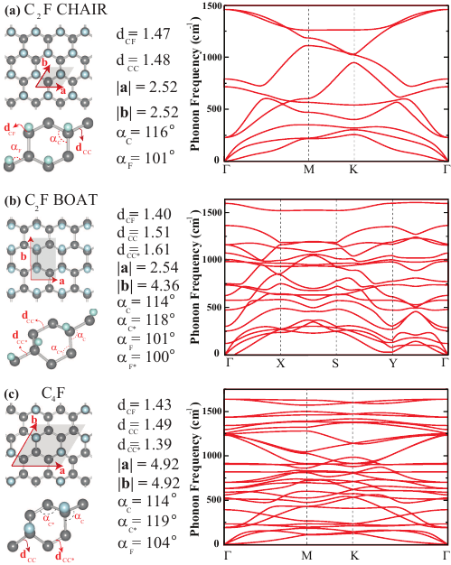
| C2F chair | 2.52 | 1.48 | 1.47 | 0.29 | 116 | 101 | metal | metal | -89.22 | 0.09 | 1.7(0.9) | 1.2 | 8.6/5.6 | 280 | 0.18 |
| C2F boat | 2.54(4.36) | 1.51/1.61 | 1.40 | 0.42 | 114/118 | 100/101 | 1.57 | 5.68 | -92.48 | 0.91 | 2.5(1.6) | 2.4 | 7.9/5.1 | 286(268) | 0.05 |
| C4F | 4.92 | 1.49/1.39 | 1.43 | 0.34 | 114/119 | 104 | 2.93 | 5.99 | -87.68 | 1.44 | 3.0(2.7) | 3.5 | 8.1/5.6 | 298 | 0.12 |
In earlier theoretical studies, charlier ; boukhvalov2 ; robinson the total energies and/or binding energies were taken as criteria for whether a given CnF structure exists. Even if a CnF structure seems to be in a minimum on the Born- Oppenheimer surface, its stability is meticulously examined by calculating frequencies of all phonon modes in BZ. Here we calculated phonon dispersions of most of optimized CnF structures. We found C4F, C2F boat, C2F chair (See Fig. 1) and CF chair (See Fig. 2) structures have positive frequencies throughout the Brillouin zone indicating their stability.
Some of phonon branches of CnF structures (for example, CF boat) have imaginary frequencies and hence are unstable, in spite of the fact that their structures can be optimized. The possibility that these unstable structures can occur at finite and small sizes is, however, not excluded. For stable structures, the gap between optical and acoustical branches is collapsed, since the optical branches associated with the modes of C-F bonds occur at lower frequencies. This situation is in contrast with the phonon spectrum of graphane, graphane-h1 where optical modes related with C-H bonds appear above the acoustical branches at 2900 cm-1.
The formation energy of fluorination is defined as in terms of the total ground state energies of optimized structures of graphene and fluorinated graphenes at different composition, respectively, , , and the total ground state energy of single carbon atom, , of F2 molecule and F atom, and . Similarly, the binding energy of F atom relative to graphene including F-F coupling is and without F-F coupling . Here is the total energy of suspended single or double layers of F occupying the same positions as in CnF. The desorption energy, is the energy required to remove one single F atom from the surface of CnF. and are numbers of F2 molecules and F atoms, respectively. The total energies are calculated in periodically repeating supercells comprising 8 carbon atoms and keeping all the parameters of calculations described above using spin-polarized as well as spin unpolarized LDA. Lowest (magnetic or nonmagnetic) total energy is used as ground state total energy.
Fluorographene (CF), where F atoms are bound to each C atom of graphene alternatingly from top and bottom sides is energetically most favorable structure. Upon full fluorination, the planar honeycomb structure of C atoms becomes buckled (puckered) and C-C bond length increases by 10%. At the end, while planar -bonding of graphene is dehybridized, the buckled configuration is maintained by -like rehybridization. In Table 1, the calculated lattice constants, internal structural parameters, relevant binding energies and energy band gaps of stable CnF structures are compared with those of bare graphene and CH.graphane-h1 Notably, internal parameters (such as , C-C bond length) as well as lattice constants of various CnF structures vary with F coverage, . CF, has highest values for , , and given in Table 1; those of C4F are second highest among stable CnF structures.
Since Raman spectrum can convey information for a particular structure and hence can set its signature, calculated Raman active modes of stable C4F and CF structures together with those of graphene and CH are also indicated in Fig. 2 (c) and (d). It is known that the only characteristic Raman active mode of graphene at 1594 cm-1 is observed so far. r-graphene Similarly, for CH the mode at 1342 cm-1 is observed.novo-graphane One of two Raman active modes of C4F at 1645 cm-1 seems to be observed.robinson In compliance with the theory, ferrari phonon branches of all these observed modes exhibit a kink structure. However, none of the Raman active modes of CF revealed in Fig. 2 has been observed yet. Raman spectroscopy in the low frequency range may be useful in identifying experimental structures.
IV Electronic Structures
Energy bands, which are calculated for the optimized C4F, C2F boat, C2F chair and CF chair structures are presented in Fig. 3 and Fig. 4 structures, respectively. The orbital projected densities of states (PDOS) together with the total densities of states of these optimized structures are also presented. Analysis of the electronic structure can also provide data to reveal the observed structure of fluorinated graphene. As seen in Table 1, stable CnF structures have LDA band gaps ranging from 0 eV to 2.96 eV. Surprisingly, C2F chair structure is found to be a metal owing to the odd number of valance electrons in the primitive unit cell. Even if various measurements on the band gap of fluorinated graphene lie in the energy range from 68 meVcheng to 3 eV,nair these calculated band gaps are underestimated by LDA. Incidentally, the band gaps change significantly after they are corrected by various self-energy methods. In fact, the correction using GW0 self-energy method predicts a rather wide band gap of 7.49 eV for CF. The corrected band gaps for C2F boat structure and C4F are 5.68 eV and 5.99 eV, respectively. It should be noted that the GW0 self-energy method has been successful in predicting the band gaps of 3D semiconductors.hse06
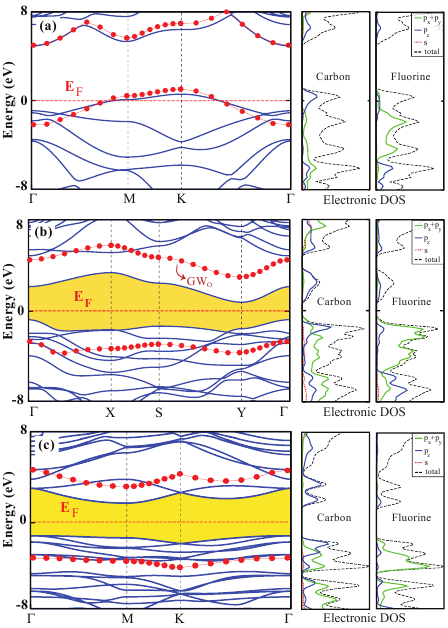
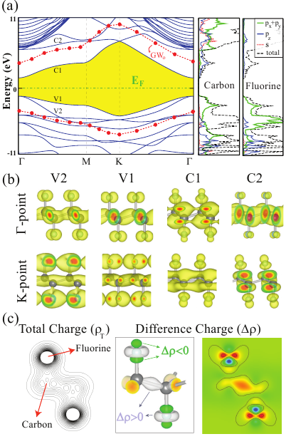
While predicting much larger band gap for CF, the measured band gap of 3 eV reported by Nair et al.nair marks the serious discrepancy between theory and experiment. The character of the band structure of CF are revealed from the analysis of projected density of states as well as charge densities of specific bands in Fig. 4 (b). Conduction band edge consists of the antibonding combination of -orbitals of F and C atoms. The -orbitals of C atoms by themselves, are combined to form -bands. The bands at the edge of the valence band are derived from the combination of C- and F- orbitals. The total contribution of C orbitals to the valence band can be viewed as the contribution of four tetrahedrally coordinated -like hybrid orbitals of - and -orbitals of C atoms. However, the deviation from tetrahedral coordination increases when increases or single side is fluorinated. As a matter of fact, the total density of states presented in Fig. 3 and Fig. 4 mark crucial differences. In this respect, spectroscopy data is expected to yield significant information regarding the observed structures of fluorinated graphenes.
The contour plots of the total charge density, , in the F-C-C-F plane suggests the formation of strong covalent C-C bonds from the bonding combination of two C- hybrid orbitals. The difference charge density, (which is obtained by subtracting the charges of free C and free F atoms situated at their respective positions in CF), indicates charge transfer to the middle of C-C bond and to F atom, revealing the bond charge between C atoms and ionic character of C-F bond. However, the value of charge transfer is not unique, but diversifies among different methods of analysis.charge-analysis Nevertheless, the direction of calculated charge transfer is in compliance with the Pauling ionicity scale and is corroborated by calculated Born effective charges, which have in-plane () and out-of-plane () components on C atoms, , and on F atoms , .
Finally, we note that perfect CF is a nonmagnetic insulator. However, a single isolated F vacancy attains a net magnetic moment of 1 Bohr magneton () and localized defect states in the band gap. Creation of an unpaired - electron upon F vacancy is the source of magnetic moment. However, the exchange interaction between two F-vacancies calculated in a (7x7x1) supercell is found to be nonmagnetic for the first nearest neighbor distances due to spin pairings. Similar to graphane,graphane-h1 ; graphane-h2 it is also possible to attain large magnetic moments on F-vacant domains in CF structures.
V Elastic Properties of CF
Having analyzed the stability of various CnF structures with 1,2 and 4, we next investigate their mechanical properties. The elastic properties of this structure can conveniently be characterized by its Young’s modulus and Poison’s ratio. However, the in-plane stiffness is known to be a better measure of the strength of single layer honeycomb structures, since the thickness of the layer cannot be defined unambiguously. Defining as the equilibrium area of a CnF structures, the in-plane stiffness is obtained as , in terms of strain energy and uniaxial strain .graphane-m The values of in-plane stiffness , and Poisson’s ratio , calculated for stable CnF structures are given in Table 1 together with the values calculated for graphene and graphane. For example, the calculated values of CF are =250 J/m2 and =0.14. It is noted that increases with . For CF (i.e. ), the in-plane stiffness is close to that calculated for CH. It appears that either the interaction between C-F bonds in CF (or the interaction between C-H bonds in CH) does not have significant contribution to the in-plane stiffness. The main effect occurs through dehybridization of bonds of graphene through the formation C-F bonds (or C-H bonds).
A value of Young’s modulus around 0.77 can be calculated by estimating the thickness of CF as =3.84 Å, namely the sum of the thickness of graphene (3.35 Å) and buckling, (0.49 Å). This value is smaller, but comparable with the value proposed for graphene, i.e. 1 . Here the contribution of C-F bonds to the thickness of CF is neglected, since the interaction between C-F bonds has only negligible effects on the strength of CF.
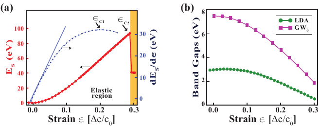
In Fig. 5 the variation of strain energy and its derivative, , with strain, are presented in both elastic and plastic regions. Two critical strain values, and , are deduced. The first one, , is the point where the derivative curve attains its maximum value. This means that the structure can be expanded under smaller tension for higher values of strain. This point also corresponds to phonon instabilitygraphane-m where the longitudinal acoustic modes start to become imaginary for . The second critical point, ), corresponds to the yielding point. Until this point the honeycomb like structure is preserved, but beyond it the plastic deformation sets in. We note that for the system is actually in a metastable state, where the plastic deformation is delayed. Under the long wavelength perturbations, vacancy defects and high ambient temperature approaches to . In fact, our further molecular dynamics simulations show that 0.17 at 300K and to 0.16 at 600K. In the presence of periodically repeating F-vacancy and C+F-divacancy, the value of is also lowered to 0.21 and 0.14, respectively. Apart from phonon instability occurring at high , the band gap is strongly affected under uniform expansion. In Fig. 5(b) we show the variation of LDA and - corrected band gaps under uniform expansion. The LDA gap slightly increases until and then decreases steadily with increasing . The -corrected band gap essentially decreases with increasing strain. For example, its value decreases by 38% for .
VI Conclusions
Present analysis of fluorinated graphenes shows that different CnF structures can form at different level of F coverage. Calculated properties of these structures, such as lattice parameter, distance, band gap, density of states, work function, in plane stiffness , Poisson’s ratio and surface charge, are shown to depend on or coverage . Relevant data reported in various experiments do not appear to agree with the properties calculated any one of the stable CnF structures. This finding lets us to conclude that domains of various CnF structures can form in the course of the fluorination of graphene. Therefore, the experimental data may reflect a weighted average of diverse CnF structures together with extended defects in grain boundaries. In this respect, imaging of fluorinated graphene surfaces by scanning tunneling and atomic force microscopy, as well as x-ray photoemission spectroscopy is expected to shed light on the puzzling inconsistency between theory and experiment.
Finally, our results show a wide range of interesting features of CnF structures. For example, a perfect CF structure as described in Fig. 2 is a stiff, nonmagnetic wide band gap nanomaterial having substantial surface charge, but attains significant local magnetic moment through F-vacancy defects. Moreover, unlike graphane, half fluorinated graphene with only one side fluorinated is found to be stable, which can be further functionalized by the adsorption of adatoms to other side. For example, hydrogen atoms adsorbed to other side attain positive charge and hence permanent transversal electric field, which can be utilized to engineer electronic properties.
VII ACKNOWLEDGMENTS
This work is supported by TUBITAK through Grant No:108T234. Part of the computational resources has been provided by UYBHM at ITU through grant Grant No. 2-024-2007. We thank the DEISA Consortium (www.deisa.eu), funded through the EU FP7 project RI-222919, for support within the DEISA Extreme Computing Initiative. S. C. acknowledges the partial support of TUBA, Academy of Science of Turkey. The authors would also like to acknowledge the valuable suggestions made by D. Alfe.
References
- (1) K. S. Novoselov, A. K. Geim, S. V. Morozov,D. Jiang, Y. Zhang, S. V. Dubonos, I. V. Grigorieva, A. A. Firsov, Science 306, 666 (2004).
- (2) A. K. Geim, K. S. Novoselov, Nat. Mater. 6, 183 (2007).
- (3) C. Berger, Z. Song, T. Li, X. Li, A. Y.Ogbazghi, R. Feng, Z. Dai, A. N. Marchenkov, E. H. Conrad, P. N. First, and W. A. de Heer, Science 312, 1191 (2006).
- (4) M. I. Katsnelson, K. S. Novoselov, and A. K. Geim, Nat. Phys. 2, 620 (2006).
- (5) H. Şahin, R. T. Senger and S. Ciraci, J. Appl. Phys. 108, 074301 (2010).
- (6) D. A. Dikin, S. Stankovich, E. J. Zimney, R. D. Piner, G. H. B. Dommett, G. Evmenenko, S. T. Nguyen and R. S. Ruoff, Nature 448, 457 (2007).
- (7) D. C. Elias, R. R. Nair, T. M. G. Mohiuddin, S. V. Morozov, P. Blake, M. P. Halsall, A. C. Ferrari, D. W. Boukhvalov, M. I. Katsnelson, A. K. Geim and K. S. Novoselov, Science 323, 610 (2009).
- (8) J. O. Sofo, A. S. Chaudhari and G. D. Barber, Phys. Rev. B 75, 153401 (2007).
- (9) D. W. Boukhvalov, M. I. Katsnelson, A. I. Lichtenstein, Phys. Rev. B 77, 035427 (2008).
- (10) H. Şahin, C. Ataca and S. Ciraci, Appl. Phys. Lett. 95, 222510 (2009).
- (11) H. Şahin, C. Ataca and S. Ciraci, Phys. Rev. B 81, 205417 (2010).
- (12) M. Topsakal, S. Cahangirov and S. Ciraci, Appl. Phys. Lett. 96, 091912 (2010).
- (13) J.-C. Charlier, X. Gonze and J. -P. Michenaud, Phys. Rev. B 47, 16152 (1993).
- (14) Y. Takagi and K. Kusakabe, Phys. Rev. B, 65, 121103 (2002).
- (15) D. W. Boukhvalov, Physica E, 43, 199 (2010).
- (16) S. -H. Cheng, K. Zou, F. Okino, H. R. Gutierrez, A. Gupta, N. Shen, P. C. Eklund, J. O. Sofo, and J. Zhu, Phys. Rev. B 81, 205435 (2010).
- (17) J. T. Robinson, J. S. Burgess, C. E. Junkermeier, S. C. Badescu, T. L. Reinecke, F. K. Perkins, M. K. Zalalutdniov, J. W. Baldwin, J. C. Culbertson, P. E. Sheehan, and E. S. Snow, Nano Lett. 10, 3001 (2010).
- (18) R. R. Nair, W. Ren, R. Jalil, I. Riaz, V. G. Kravets, L. Britnell, P. Blake, F. Schedin, A. S. Mayorov, S. Yuan, M. I. Katsnelson, H.-M. Cheng, W. Strupinski, L. G. Bulusheva, A. V. Okotrub, I. V. Grigorieva, A. N. Grigorenko, K. S. Novoselov, A. K. Geim, Small 6, 2877 (2010).
- (19) O. Leenaerts, H. Peelaers, A. D. Hernandez-Nieves, B. Partoens, and F. M. Peeters, Phys. Rev. B 82, 195436 (2010).
- (20) F. Withers, M. Dubois, and A. K. Savchenko, Phys. Rev. B 82, 073403 (2010).
- (21) M. Klintenberg, S. Lebegue, M. I. Katsnelson, and O. Eriksson, Phys. Rev. B 81, 085433 (2010).
- (22) E. Munoz, A. K. Singh, M. A. Ribas, E. S. Penev, and B. I. Yakobson, Diamond Relat. Mater. 19, 368 (2010).
- (23) G. Kresse and J. Hafner, Phys. Rev. B 47, 558 (1993); G. Kresse and J. Furthmüller, Phys. Rev. B 54, 11169 (1996).
- (24) D. M. Ceperley and B. J. Alder, Phys. Rev. Lett. 45, 566, (1980).
- (25) P. E. Blochl, Phys. Rev. B 50, 17953 (1994).
- (26) M. Shishkin and G. Kresse, Phys. Rev. B 74, 035101 (2006).
- (27) P. Giannozzi et al. J. Phys. Condens. Matter 21, 395502 (2009).
- (28) Y. Gan, L. Sun, and F. Banhart, Small 4, 587 (2008).
- (29) C. Ataca, E. Akturk, H. Şahin and S. Ciraci, J. Appl. Phys. 109, 013704 (2011).
- (30) A. C. Ferrari, J. C. Meyer, V. Scardaci, C. Casiraghi, M. Lazzeri, F. Mauri, S. Piscanec, D. Jiang, K. S. Novoselov, S. Roth, and A. K. Geim, Phys. Rev. Lett. 97, 187401 (2006).
- (31) S. Piscanec, M. Lazzeri, F. Mauri, A. C. Ferrari, and J. Robertson, Phys. Rev. Lett. 93, 185503 (2004).
- (32) HSE hybrid functional implemented in VASP [K. Hummer, J. Harl, G. Kresse, Phys. Rev. B 80, 115205 (2009)] is demonstrated to be as succesful as GW0 self-energy correction method in predicting the band gaps of bulk 3D crystals. Consistently, for 2D honeycomb structures HSE is found to yield smaller values than those of GW0. For example, while HSE predicts the band gap of CF as 4.86 eV, GW0 gives 7.49 eV. Similar trends are also found for CH and 2D Boron Nitride (BN). HSE and GW0 corrected band gaps of CH (BN) band gaps are 4.51 (5.74) and 5.97 (6.86) eV, respectively.
- (33) H. Şahin, S. Cahangirov, M. Topsakal, E. Bekaroglu, E. Aktürk, R. T. Senger, and S. Ciraci, Phys. Rev. B 80, 155453 (2009).
- (34) For example, Bader [G. Henkelman, A. Arnaldsson, H. Jonsson, Comput. Mater. Sci.36, 254-360 (2006)], Löwdin [P.-O. Löwdin, J. Chem. Phys. 18, 365 (1950)] and Mulliken [R. S. Mulliken, J. Chem. Phys. 23, 1841 (1955)] methods predict charge transfer from C to F atoms, respectively, 0.59, 0.19 and 0.06 electrons. Further analysis by calculating planarly averaged charge density of CF and of free C and F atoms, where the charge due to the tails of orbitals are carefully accounted deduces that the total of 0.11 electrons are transferred from buckled graphene to each F atom.