Coupling of excitons and defect states in boron-nitride nanostructures
Abstract
The signature of defects in the optical spectra of hexagonal boron nitride (BN) is investigated using many body perturbation theory. A single BN-sheet serves as a model for different layered BN-nanostructures and crystals. In the sheet we embed prototypical defects such as a substitutional impurity, isolated Boron and Nitrogen vacancies, and the di-vacancy. Transitions between the deep defect levels and extended states produce characteristic excitation bands that should be responsible for the emission band around eV, observed in luminescence experiments. In addition, defect bound excitons occur that are consistently treated in our ab initio approach along with the “free” exciton. For defects in strong concentration, the co-existence of both bound and free excitons adds sub-structure to the main exciton peak and provides an explanation for the corresponding feature in cathodo and photo-luminescence spectra.
pacs:
71.35.-y 71.55.-II Introduction
Boron nitride crystals and nano structures are excellent wide band gap materials for the realization of UV-lasers.patent Defects formed during the BN-synthesis or introduced as impurities can bind excitons and act as centers for their recombination. This leads to (desired or undesired) luminescence bands and losses in the photon frequency range of interest. In fact, recent experiments watanabe1 ; watanabe2 ; watanabe3 ; PhysRevB.75.085205 ; Museur2008 ; PhysRevB.78.155204 ; loiseau ; PhysRevB.77.235422 have given evidence that defects strongly effect the luminescence of BN-based materials. In order to achieve optimal optical properties, the relevant defects have to be identified such that methods can be devised to tune their concentration in the material.
Boron nitride (BN) is known to exist in three different crystals structures, namely hexagonal BN (h-BN), cubic BN (c-BN), and wurtzite BN (w-BN). Among these structures, h-BN is the stable one at room temperature and ambient pressure. Like graphite, it consists of stacked BN-layers with a honeycomb structure. BN nanostructuresxblasereview ; wirtz_review ranging from single and multi-wall nanotubes to BN-fullerens and nanocones can be envisaged as having been tailored from a single BN sheet. Unlike in graphite, the partially ionic character of the BN bond results in a wide band-gap of about 6.5 eV for bulk h-BNArnaud2006 . The combination of a large gap with a strong electron-hole attraction makes the optical properties of BN nanostructures largely independent of the layer arrangement.PhysRevLett.96.126104 ; wirtz_review A single layer of h-BN is thus a generic system for studying the optical properties of crystalline and nanostructured BN including the exciton-defect interaction.
Detailed experiments on the cathodo and photo-luminescence of h-BN crystals and BN nanotubes have been performed in the recent years watanabe1 ; watanabe2 ; watanabe3 ; PhysRevB.75.085205 ; Museur2008 ; PhysRevB.78.155204 ; loiseau ; PhysRevB.77.235422 ; zhi:213110 . The origin of some of the features in the BN luminescence spectra remains unsettled. For instance, the occurrence of a defect-related emission band at eV, composed of regularly spaced peaks compatible with phonon replicasPhysRevB.75.085205 ; PhysRevB.78.155204 ; jaffrennou:116102 , can be associated with a deep level impurity. However, the defect that is responsible for this deep level has not yet been identified. Furthermore, the emission band at eV shows different sub-peaks on the low energy side. The origin of its sub-structure is unclear, since the main peak can be understood as being due to the recombination of a Frenkel-type excitonArnaud2006 with a degenerate recombination line.PhysRevLett.96.126104 ; PhysRevLett.100.189701 Interpretations of the experimental findings are based on different mechanisms: quasi-donor-acceptor pairsMuseur2008 , excitons coupled with structural defects PhysRevB.77.235422 ; jaffrennou:116102 , breaking of the exact hexagonal symmetry (e.g., by the presence of defects) PhysRevLett.100.189701 , or a dynamical Jahn-Teller effectPhysRevB.79.193104 (symmetry breaking due to geometry relaxation in the excited state).
Theoretical works on defects in BN-structures have so far focused on the electronic and structural properties of point defects azevedo ; PhysRevB.67.113407 ; PhysRevB.63.125205 ; hou:076103 ; PhysRevB.81.075125 ; PhysRevB.75.193409 ; PhysRevB.76.014405 . The abundance (related to the formation energy) and stability of different defects has been addressed with detailed density-functional theory (DFT) calculations.PhysRevB.63.125205 ; PhysRevB.80.161404 ; PhysRevB.66.014112 ; PhysRevB.81.153407 ; PhysRevB.75.094104 ; zobelli . The position of deep levels within the fundamental band gap has been calculated on the DFT level. However, DFT calculation suffer from the well-known underestimation of the band-gap. Therefore, besides the neglect of the strong excitonic effects in BN, (de)excitation spectra based on DFT energy levels may not be reliable enough for comparison with experimental spectra.
In the present paper we address the optical properties of point defects in BN going beyond the approximation of DFT. We focus on a substitutional carbon impurity on the nitrogen site, the isolated vacancies and the BN di-vacancy that are common defects in BN. We will demonstrate that defects are responsible for the emission lines around eV. Their presence can also explain the experimentally observed splitting of the main exciton peak. The paper is organized as follows: in section II we summarize the computation methods employed in this work; in section III we present the ground state results and the quasi-particle(QP) band structures; in section IV we investigate the role of defects on the optical properties and finally in section V we compare our results with experiments.
II Computational Methods
Density functional theory (DFT) within the local spin density (LSDA) or gradient corrected approximations (GGA) for the exchange-correlation energy has been widely used to study defects in semiconductors and insulators. Although DFT is in principle exact, it is limited to the ground state and as a closed expression for the exchange-correlation energy functional is unknown, approximations like the LSDA or GGA have to be employed. Albeit theoretically well-founded, these approximate functionals bear inherent limitations like the well-known band gap problem which concomitantly affect the prediction of defect levels, in particular in wide band gap insulators. In the last years, many-body perturbation theory within the GW approximationAulbur19991 has become a valid and accurate alternative to predict defects properties in semiconductors and insulators PhysRevLett.102.026402 ; PhysRevB.81.113201 ; PhysRevB.51.7464 starting from the DFT ground state. Moreover, in going beyond the ground state, the optical properties of defects and the host insulator can be addressed by including the electron-hole interaction in the excited state via the Bethe-Salpeter equation (BSE) strinati2 ; PhysRevB.77.115118 ; bockstedte .
Here we use this approach to study the role of prototypical defects in the optical properties of BN nanostructures: a substitional carbon impurity on the nitrogen sublattice (), the boron vacancy (), the nitrogen vacancy () and the boron-nitrogen di-vacancy (). Calculations proceed in three steps: first we obtain the DFT ground state employing the LSDA approximation and a plane wave pseudopotential method,pwscf (see DFT, for details). Second we evaluate the quasi-particle band structure within the G0W0Aulbur19991 ; RevModPhys.74.601 ; hybert approach and third we address the optical spectra via the BSE.strinati A very large supercellDFT is employed to accommodate the defect and to enable at the same time the description of defect bound and free excitons. This becomes possible due to the strong localization of the bulk exciton state in h-BN,Arnaud2006 in the layer, and tubes PhysRevLett.96.126104 ; park2006 .
As it has been shown that a large class of impurities, when introduced into h-BN, is in a spin-polarized state and acquires a local magnetic momentPhysRevB.76.014405 , we have performed spin-polarized calculations for the , , and cases while this was not necessary for the di-vacancy that does not display a net spin polarization. The quasi-particle properties have been calculated starting from the Kohn-Sham Hamiltonian and orbitals within the G0W0 approximationGW :
| (1) |
where and is the LSDA exchange-correlation functional, are the Kohn-Sham eigenvalues, and is the renormalization factorAulbur19991 . The screened electron-electron interaction has been evaluated within the random-phase approximation (RPA) in terms of the dielectric function using a plasmon-pole model.epsilon Neutral excitations are investigated on the basis of the quasiparticle spectrum by solving the Bethe-Salpeter equation (see BSE, for details). Excitonic effects are analysed through a comparison of the absorption spectra for independent particles with absorption spectra where electron-hole attraction is included on the level of the BSE.
As we are studying an isolated monolayer employing three-dimensional periodic boundary conditions, the size of the quasi particle energies and the energy of the electron-hole attraction will depend on the inter-sheet distance. In Ref. PhysRevLett.96.126104, we had shown that the value of the gap of the pure h-BN sheet is 0.6 eV higher for an inter-sheet distance is 80 a.u. than for an inter-sheet distance of 20 a.u. (value which we are using in the calculations presented here). At the same time we had observed an increase of the exciton binding energy with increasing inter-sheet distance that almost exactly cancels the variation of the band-gap. We expect a similar cancellation effect in the presence of defects but cannot exclude a minor effect of the inter-sheet distance on the absolute position of defect peaks.
III DFT-ground state and Quasi-particle states
In this section we address the electronic and geometric structure of the four defects and then compare the DFT-electronic structure with the quasiparticle states obtained from G0W0 calculations.
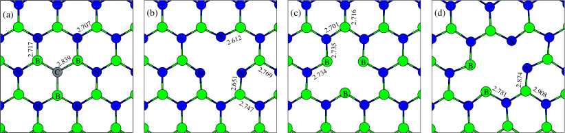
In Fig. 1 the equilibrium geometry of the C and the vacancies V,V and V is shown along with the BN bond distances in the vicinity of the defect center. In the case of subsitutional impurity all the first neighbor B atoms of undergo a small symmetry conserving outward relaxation of 0.113 a.u. (4% of the BN-bond distance) with respect to the ideal lattice positions. The defect retains its threefold symmetry. In the case of and the the outward displacement of the first-neighbor atoms is larger. More importantly, in agreement with Ref. PhysRevB.76.014405, , we find that a (pseudo) Jahn-Teller effect breaks the three-fold symmetry slightly. In the di-vacancy case, the three-fold symmetry is already reduced to a mirror symmetry by the defect configuration itself. We observed that the first N and B neighbors decrease their mutual distance upon relaxation, as shown in Fig. 1d. The defect geometries found here are in good agreement with those reported in Ref. PhysRevB.63.125205, and azevedo, .
As established already in earlier work, the C and the vacancies possess localized defect levels in the band gap. Here we briefly review the electronic structure of the defects as obtained in DFT-LSDA and then compare it with the quasiparticle states obtained on the level of the G0W0 approximation where the DFT band gap-error is corrected. Since the prediction of defect emission and absorption spectra hinges on the defect level positions, a correct prediction of these quantities is a crucial point for the investigation of optical properties. The defect levels as obtained within the DFT-L(S)DA are reported in the left panel of Fig. 2.
In the case of the defect levels arise from the three bonds of the substitutional carbon impurity with its boron neighbors. These bonds combine into two fully occupied states located within the valence band and a third half-occupied localized state within the band gap. As a result of the occupation with only one electron there is a spin-splitting of eV between the occupied (spin-up) and unoccupied (spin-down) state.
The situation is more complex for the boron vacancy. In this case a two-fold degenerate and a non-degenerate defect state are formed from the unpaired orbitals at the three nitrogen neighbors. In agreement with Ref. PhysRevB.66.014112, ; PhysRevB.63.125205, ; zobelli, , these defect levels are located within the band gap. In the neutral vacancy the two-fold degenerate level is occupied by three electrons and the non-degenerate level remains empty. Due to the Jahn-Teller distortion a small splitting of the degenerate level arises in addition to the exchange-splitting of the half- and unoccupied states. behaves as a triple acceptor.
For we obtain a half-filled level in the band gap, and two un-occupied levels almost degenerate in energy with the conduction bands. Due to spin-splitting their counter parts of opposite spin are found as resonances in the conduction band. Finally, in the case of the di-vacancy V, there are four orbitals originating from the two boron and nitrogen neighbors. Only three are located in the band gap, one being occupied by two electrons and the upper two remaining empty.
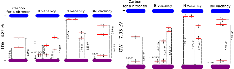
The above picture obtained from the Kohn-Sham eigenvalues gives a qualitative description of the defect levels in the band gap. The position of the states is, however, quantitatively affected by the LSDA-band gap error and the approximate treatment of exchange with this XC-functional as discussed above. Furthermore, the ordering of occupied and unoccupied states on the Kohn-Sham level may be different from that of the “true” quasi-particle energy levels (see e.g. Aulbur19991, ). The G0W0 method yields true quasiparticle energies and an improved description of exchange and screening effects. Due to the reduced dimensionality of the BN mono-layer there is an incomplete screening of the Coulomb interaction, such that the quasi-particle corrections are expected to be quite large. We calculated the quasi-particle band structure for all the cases considered above. The calculated band gap is in agreement with the results of Ref. PhysRevLett.96.126104, . In the right panel of Fig. 2 the position of the defect quasi particle energies within the band gap is shown schematically. The G0W0 corrections to the LSDA levels depend on the orbital occupation and on the wave-function characterAulbur19991 . The exchange splitting between occupied and unoccupied defect levels is strongly enhanced and the ordering of defect levels within the band gap is altered in some cases. In all cases we find that occupied levels are pushed closer to the valence bands and unoccupied ones closer to conduction bands. For C the spin-splitting is significantly increased from eV to eV. A large exchange splitting is also present in the case of V. For all un-occupied levels are pushed up by more then eV, depending on the character of the wave-function, and the level order is modified as well. In the case of V, un-occupied levels are found close to the conduction band edge, while the occupied ones remain in their position close to the valence band edge. This underlines the fact that the di-vacancy contains both donor and acceptor levels. The general picture obtained from G0W0 shows the clear deficiencies of the DFT-LSDA in the description of defect level positions in the case of BN, in particular, for unoccupied states. Vested with the defect quasiparticle spectrum we now turn to the optical properties.
IV Optical properties
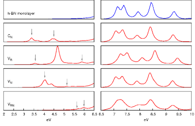
In order to discern excitonic effects on the optical properties, we present first in Fig. 3 the optical spectra in the independent particle picture (IP)convergence (i.e. without the inclusion of the electron-hole coupling). This yields an overview over relevant excitation mechanisms and later allows one to trace down the effect of the electron-hole coupling.
We start the discussion with the case of . Comparing the corresponding panel of figure 3 with the schematic representation of the defect levels in the band gap (Fig. 2) one can identify the different absorption peaks. The first band at eV is due to transitions form the extended states at the valence edge to the defect levels within the band gap; the other band at eV involves extended states below the valence band edge and defect levels. Above eV we find the bulk-like spectrum that is only slightly perturbed by the presence of the defect. For the boron vacancy V there are two bands at eV and eV that are associated with transitions from defect resonances in the valence band to the localized levels in the band gap and a series of small peaks around eV originating from valence band to defect transitions. The defect-related excitation bands of V at eV, in contrast to the previous cases, involves extended states near the conduction band edge as final states. Only the faint defect-related excitation band around eV, not visible in the figure, originates from valance band states. Another faint peak around eV is due to transitions among the defect levels in the band gap. Finally, for the V di-vacancy, we find peaks between eV and eV due to defect-defect transitions and valence-band to defect transitions, respectively.
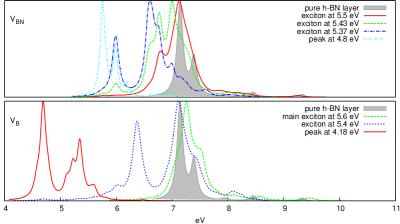
We now turn to the spectraconvergence including the electron-hole interaction via the Bethe-Salpeter equation. These are shown in Fig. 5. The inclusion of the electron-hole interaction has essentially two effects on the defect-related spectra: (i) a general red-shift of the defect excitation energies due to electron-hole attraction and (ii) a coupling of the independent particle excitations. This coupling can give rise to bound electron-hole states, the excitons. In our case the BSE leads to a red-shift of defect-defect transitions in the range from to eV depending on the character and the localization of the wavefunction. A common feature of all spectra is the large peak around 5.5 eV which corresponds to the strongly localized exciton of pure h-BNArnaud2006 ; PhysRevLett.96.126104 ; park2006 which is composed of a large number of independent electron-hole pairs. In the presence of a defect, electron-hole coupling leads to defect bound excitons besides the “free” excitons.
In the case of and , as one can see from Fig. 5, an additional small peak appears just below the main excitons. In the case of the main exciton band has three sub-peaks due to the strong defect field with reduced symmetry. In order to disentangle the nature of the different peaks, we analyze the amplitude of the electron-hole pairs that compose each of the exciton eigenstates , as a function of the energy difference of the quasiparticle states of the corresponding electron and hole states:
| (2) |
For brevity, we report only for and (see Fig. 4). The plots for the other defects show generally a similar behavior.
Comparing for the electron-hole amplitudes of the four
excitation energies with the schematic diagram of
Fig. 2, we can distinguish three kinds of excitations:
(i) transitions from valence bands or defect resonances to the defect
levels, that generate the peaks at eV, (ii) the main exciton at
eV that is entirely composed of extended states, and (iii)
a peak at eV generated by the coupling of bulk excitations
with transitions from and to defect levels in the band gap.
The and cases present a structure similar to the one discussed
above. From these results it is possible to infer three important
consequences: (i) transition from defect levels to valence/conduction
bands with an energy close to the band gap energy mixes with the bulk excitation
giving rise to an additional peak close to the main exciton; (ii)
transition between defect levels are renormalized by the
electron-hole interaction but do not mix with the bulk excitations;
(iii) the main exciton peak maintains a structure similar to the bulk
system.
The excitonic band of the di-vacancy is distinct from the other spectra as the di-vacancy possess both acceptor and donor states of low symmetry in the vicinity of the band edges. The direct transitions between acceptor and donor states give rise to the absorption peaks around eV, while the resonant coupling of transitions between the extended conduction and valence band states with donor and acceptor states splits the main exciton in three sub-peaks respectively at eV, eV and eV (see Fig. 4).
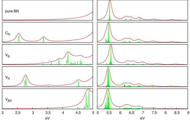
The observed side peaks to the main excitonic peak are compatible with
the fine structure observed in different luminescence experimentsPhysRevB.75.085205 ; jaffrennou:116102 ; Museur2008 ; PhysRevB.79.193104 .
V Conclusion
We have investigated the role of defects on the optical properties of BN nanostructures. We have treated four different plausible defects in a single sheet of hexagonal BN: a subsitutional carbon impurity, a boron vacancy, a nitrogen vacancy, and a BN di-vacancy. Quasi-particle effects strongly modify the defect-level positions within the band-gap and increase the exchange splitting between occupied and unoccupied levels. Electron-hole interaction (treated on the level of the the Bethe-Salpeter equation) not only leads to a strongly bound excitonic state in pure BN but also strongly renormalizes transitions from and to defect levels. This means that the peaks in the optical spectra which are related to “deep level impurities”are strongly affected by the e-e and e-h interaction and can be reliably calculated only on the level of many-body perturbation theory (as opposed to the frequently used random-phase approximation using DFT wave-functions and energies). Experimental luminescence spectra (as presented, e.g., in Ref. jaffrennou:116102, ) display a prominent peak close to eV with phonon replica on the low energy side. Comparing the four theoretical absorption spectra (Fig. 5) with the experimental luminescence spectrum, the best agreement is obtained for the Boron vacancy where the main absorption peak of the low energy regime is at 4.2 eV. The Stokes shift due to possible relaxation of the excited state is not included in our calculation and limits the comparison of experimental luminescence with theoretical absorption spectra. In the case of a strong (0.7 eV) Stokes shift, also the BN-divacancy (where a defect related absorption peak is at 4.8 eV) could be responsible for the experimental observation. The nitrogen vacancy (absorption peak at 4.5 eV) might also explain the experiment. However, in this case a second strong luminescence peak should also be observable below 3 eV which seems not to be the case in experiments.
The 1010 supercell employed in our calculations is considerably larger than the extension of the wave-function of the “free” exciton in pure h-BN. Therefore, besides the defect-related absorption peaks, our calculations also show the prominent absorption peak due to “free” excitions at 5.6 eV. This peak is doubly degenerate in the pure BN sheet. Coupling of the free exciton with one or several transitions from or to defect levels gives rise to a splitting of this peak and additional side peaks. The details of the splitting depend on the nature of the impurity but also on its periodic arrangementnotedefstack . The fine-structurewatanabe1 of the luminescence peak at 5.7 eV (with additional side peaks at 5.64 eV and 5.46 eV) can possibly be explained through our calculations which clearly display defect-related side peaks of the “free” excitonic peak. Furthermore, any kind of breaking of the exact hexagonal symmetry can lead to a splitting of the bright doubly degenerate “free” excitonic peak into two peaks and will also (for bulk h-BN) render the “dark” exciton (located 0.1 eV below the bright exciton) visible PhysRevLett.100.189701 . For reasons of computational feasibility, we have performed calculations only on point defects. Other kinds of defects such as dislocations and grain boundaries lead similarly to a breaking of symmetry and/or to the formation of localized states and could thus as well explain the fine structure of luminescence spectra one would expect a similar interaction of the “free” exciton with dangling-bond states). Indeed, Jaffrenou et al. had observed that the luminescence peaks at 5.64 eV and 5.46 eV occur mostly at grain boundaries and dislocationsjaffrennou:116102 where defect states due to dangling bonds are supposed to occur. The aim of our present study is thus not to unambiguously assign a certain type of defect to the observed luminescence spectra, but rather to show the general mechanism leading to the deep impurity levels and the formation of defect bound excitons. We also note that we did not study all possible point defects. A recent study of the chemical composition of an isolated h-BN sheet suggests the incorporation of oxygen atoms in the honeycomb latticeKrivanek . The same study also demonstrated that substitutional carbon atoms occur mostly in pairs, occupying neighboring nitrogen and boron sites. Further experimental and theoretical studies are necessary to decide if the latter two types of defects can also occur during the synthesis of BN nanostructures or if they are due to the experimental conditions in the transmission electron microscope where vacancies in the h-BN sheet are induced by the electron bombardment and may be subsequently filled by a substitutional atom.
An alternative route to symmetry breaking was proposed by Watanabe et al.PhysRevB.79.193104 . They suggested that the dynamical Jahn-Teller effect (splitting of the degenerate exciton by polaronic effects) could explain the excitonic splitting in hexagonal BN. Further experimental and theoretical studies are necessary to disentangle the two effects.
Acknowledgments
We acknowledge funding by the European Community through e-I3 ETSF project (Contract Number 211956). AR acknowledges funding by the Spanish MEC (FIS2007-65702-C02-01), ACI-promciona project (ACI2009-1036), ”Grupos Consolidados UPV/EHU del Gobierno Vasco” (IT-319-07). LW acknowledges funding by the French National Research Agency through project ANR-09-BLAN-0421-01. This work was performed using HPC resources from GENCI-IDRID (No. 100063 and No. 091827). CA thanks X. Andrade and J. Alberdi Rodriguez for the efficient computer-cluster installation in San Sebastian. This work has been supported by the project no. FIS2010-21282-C02-01 (MCINN) from Spain.
References
- (1) T. Taniguchi, K. Watanabe, Y. Kubota, and O. Tsuda, “Production of a hexagonal boron nitride crystal body capable of emitting out ultraviolet radiation,” (May 2010), patent number: US 2010/0120187 A1
- (2) K. Watanabe, T. Taniguchi, and H. Kanda, Nature Materials 3, 404 (2004)
- (3) Y. Kubota, K. Watanabe, O. Tsuda, and T. Taniguchi, Science 317, 932 (2007)
- (4) K. Watanabe, T. T. Takashi, and K. H. Kanda, Diamond and Related Materials 15, 1891 (2006)
- (5) M. G. Silly, P. Jaffrennou, J. Barjon, J.-S. Lauret, F. Ducastelle, A. Loiseau, E. Obraztsova, B. Attal-Tretout, and E. Rosencher, Phys. Rev. B 75, 085205 (Feb 2007)
- (6) L. Museur and A. Kanaev, Journal of Applied Physics 103, 103520 (2008)
- (7) L. Museur, E. Feldbach, and A. Kanaev, Phys. Rev. B 78, 155204 (Oct 2008)
- (8) P. Jaffrennou, F. Donatini, J. Barjon, J.-S. Lauret, A. Maguer, B. Attal-Tretout, and F. Ducastelle, Chemical Physics Letters 442, 372 (2007)
- (9) P. Jaffrennou, J. Barjon, T. Schmid, L. Museur, A. Kanaev, J.-S. Lauret, C. Y. Zhi, C. Tang, Y. Bando, D. Golberg, B. Attal-Tretout, F. Ducastelle, and A. Loiseau, Phys. Rev. B 77, 235422 (Jun 2008)
- (10) R. Arenal, X. Blase, and A. Loiseau, Advances in Physics 59, 101 (2010)
- (11) L. Wirtz and A. Rubio, Optical and vibrational properties of boron nitride nanotubes in B-C-N Nanotubes and Related Nanostructures, edited by Y.K. Yap, Lecture Notes in Nanoscale Science and Technology, Vol. 6 (Springer, 2009)
- (12) B. Arnaud, S. Lebègue, P. Rabiller, and M. Alouani, Phys. Rev. Lett. 96, 026402 (2006)
- (13) L. Wirtz, A. Marini, and A. Rubio, Phys. Rev. Lett. 96, 126104 (Mar 2006)
- (14) C. Zhi, Y. Bando, C. Tang, D. Golberg, R. Xie, and T. Sekigushi, Applied Physics Letters 86, 213110 (2005)
- (15) P. Jaffrennou, J. Barjon, J.-S. Lauret, B. Attal-Trétout, F. Ducastelle, and A. Loiseau, Journal of Applied Physics 102, 116102 (2007)
- (16) L. Wirtz, A. Marini, M. Gruning, C. Attaccalite, G. Kresse, and A. Rubio, Phys. Rev. Lett. 100, 189701 (May 2008)
- (17) K. Watanabe and T. Taniguchi, Phys. Rev. B 79, 193104 (May 2009)
- (18) S. Azevedo, J. R. Kaschny, C. M. C. de Castilho, and F. de Brito Mota, Eur. Phys. J. B 67, 507 (2009)
- (19) T. M. Schmidt, R. J. Baierle, P. Piquini, and A. Fazzio, Phys. Rev. B 67, 113407 (Mar 2003)
- (20) W. Orellana and H. Chacham, Phys. Rev. B 63, 125205 (Mar 2001)
- (21) Z.-L. Hou, M.-S. Cao, J. Yuan, X.-Y. Fang, and X.-L. Shi, Journal of Applied Physics 105, 076103 (2009)
- (22) F. Oba, A. Togo, I. Tanaka, K. Watanabe, and T. Taniguchi, Phys. Rev. B 81, 075125 (Feb 2010)
- (23) M. S. Si and D. S. Xue, Phys. Rev. B 75, 193409 (May 2007)
- (24) R.-F. Liu and C. Cheng, Phys. Rev. B 76, 014405 (Jul 2007)
- (25) S. Okada, Phys. Rev. B 80, 161404 (Oct 2009)
- (26) T. E. Mosuang and J. E. Lowther, Phys. Rev. B 66, 014112 (Jul 2002)
- (27) L.-C. Yin, H.-M. Cheng, and R. Saito, Phys. Rev. B 81, 153407 (Apr 2010)
- (28) A. Zobelli, C. P. Ewels, A. Gloter, and G. Seifert, Phys. Rev. B 75, 094104 (Mar 2007)
- (29) A. Zobelli, C. P. Ewels, A. Gloter, G. Seifert, O. Stephan, S. Csillag, and C. Colliex, Nano Letters 6, 1955 (2006)
- (30) W. G. Aulbur, L. Jonsson, and J. W. Wilkins, Solid State Physics (edited by H. Ehrenreich and F. Spaepen), Academic press 54, 1 (1999)
- (31) P. Rinke, A. Janotti, M. Scheffler, and C. G. Van de Walle, Phys. Rev. Lett. 102, 026402 (Jan 2009)
- (32) S. Lany and A. Zunger, Phys. Rev. B 81, 113201 (Mar 2010)
- (33) M. P. Surh, H. Chacham, and S. G. Louie, Phys. Rev. B 51, 7464 (Mar 1995)
- (34) H. J. Mattausch, W. Hanke, and G. Strinati, Phys. Rev. B 27, 3735 (Mar 1983)
- (35) Y. Ma and M. Rohlfing, Phys. Rev. B 77, 115118 (Mar 2008)
- (36) M. Bockstedte, A. Marini, O. Pankratov, and A. Rubio, Phys. Rev. Lett. 105, 026401 (2010)
- (37) P. Giannozzi and al., J. Phys. Condens. Matter 21, 395502 (2009), http://www.quantum-espresso.org
- (38) All DFT calculations have been performed using a 1010 supercell containing atoms. The distance between the BN-sheet was 20 a.u. A single k-point was used. We used the exchange-correlation functional of Ref. ceperley, . For the calculations, we used the PWSCF codepwscf with Troullier-Martins pseudopotetials troullier and a plane wave cutoff of Ry. All the atomic structures considered in the paper were relaxed using the Broyden–Fletcher–Goldfarb–Shanno (BFGS) algorithm and a convergence threshold for the forces of a.u. The 1010 k-point sampling of the elementary cell (which corresponds to the 11 sampling of the 1010 supercell) does not contain the high-symmetry point K, the point with the minimum direct gap. Therefore, the reported LDA gap of eV in Fig. 2 is slightly larger than the converged value eVwirtz_review .
- (39) G. Onida, L. Reining, and A. Rubio, Rev. Mod. Phys. 74, 601 (Jun 2002)
- (40) M. S. Hybertsen and S. G. Louie, Phys. Rev. B 34, 5390 (1986)
- (41) G. Strinati, Rivista del nuovo cimento 11, 1 (1988)
- (42) C.-H. Park, C. D. Spataru, and S. G. Louie, Phys. Rev. Lett. 96, 126105 (2006)
- (43) Non-self consistent GW calculations have been performed starting from DFT-LDA wave-functions, using a plasmon pole approximation for the dielectric constant epsilon , with the code YAMBOyambo . We use a single k-point, 3000 bands for expanding the Green’s function, 40.000 G-vectors for the exchange and 35.000 for the correlation part of the self-energy. In contrast to Ref. PhysRevLett.96.126104, we did not add any scissor operator to correct the underestimation of the band gap in the approximation.
- (44) The same dielectric constant has been employed in all the cases with and without defects, both for quasi-particle and Bethe-Salpeter equation. The dielectric constant has been calculated in the pure system, using 3000 bands, 3833 G-vectors for the dielectric matrix, and 35.000 G-vectors for the wave-functions entering in the calculation.
- (45) The optical spectra have been calculated using the Bethe-Salpeter equation (BSE) strinati , with bands 300 to 500 (all and bands of the 1010 supercell), a eV cutoff on the electron-hole pair energy entering in the BSE and 20.000 G-vectors for the electronic wave-functions.
- (46) The independent-particle (IP) spectra are obtained for the 11 k-point set (corresponding to a 1010 sampling of the elementary unit cell) and are not fully converged with respect to k-point sampling for transitions involving extended band states, despite of the large supercells employed in the present calculations. Since we are only concerned with transitions involving localized defects levels, this is irrelevant for the analysis of excitation mechanism conducted here. Moreover we verified that peaks due to defects transition do not change increasing the number of k-points. In the BSE case, the main exciton collects most of the oscillator strengths. This speeds up the k-point convergence of the spectra and makes the presented spectra almost converged, contrary to the IP ones. In both cases IP and BSE we always considered the polarization parallel to the sheet.
- (47) In our simulation, we use a 60 degree unit cell which corresponds to a trigonal ordering of the defects. If a 90 degree super-cell was chosen, the ordering of the defects would be rectangular. Only in the limit of very large unit-cells, the splitting of the excitonic peak will be independent of the defect ordering and correspond to the coupling of a “free excitons” with an isolated defect. However, with the present computational ressources, we cannot reach the limit of isolated impurities by increasing the super-cell.
- (48) O. Krivanek, M. Chisholm, V. Nicolosi, T. Pennycook, G. Corbin, N. Dellby, M. Murfitt, C. Own, Z. Szilagyi, M. Oxley, S. Pantelides, and S. Pennycook, Nature 464, 571 (2010)
- (49) D. M. Ceperley and B. J. Alder, Phys. Rev. Lett. 45, 566 (1980)
- (50) N. Troullier and J. L. Martins, Phys. Rev. B 43, 1993 (1991)
- (51) A. Marini, C. Hogan, M. Gruning, and D. Varsano, Comp. Phys. Comm. 180, 1392 (2009), http://www.yambo-code.org