Background Free Measurement of the Spectra of Low Energy Electrons Emitted as a Result of Auger Transitions in Metals
Abstract
Positron annihilation induced Auger electron spectroscopy was used to obtain Cu and Au Auger spectra that are free of primary beam induced background by impinging the positrons at energy below the secondary electron emission threshold. The removal of the core electron via annihilation in the PAES process resulted in the elimination of post-collision affects. The spectrum indicates that there is an intense low energy tail (LET) associated with the Auger peak that extends all the way to eV. The LET has been interpreted as being due to processes in which the filling of the core by a valence electron results in the ejection of two or more valence electrons which share the energy of the otherwise Auger electron
pacs:
78.70.Bj, 82.80.Pv, 68.49.-h, 79.20.Hx, 79.60.BmI Introduction
Electron and X-ray induced Auger electron spectroscopy (EAES and XAES) are extremely sensitive to the composition and chemistry of the surface ramaker:1614 ; PhysRevLett.94.038302 ; PhysRevLett.93.206802 owing to the short inelastic mean free path of electrons () emitted in the Auger energy range (- eV) tougaard1988quantitative ; seah1972quantitative . Both these techniques use an incident beam energy greater than the ionization energy of the core electron () that is removed in order to initiate the Auger process. The energy of the emitted electron as a result of filling up of the initial hole is less than due to the energy associated with the two hole final state of the Auger process. Consequently, the Auger peaks in EAES and XAES are superimposed upon a background composed of an electron cascade Seah1969132 ; Sickafus1977SecE2 ; SickafusSecE1 caused by the inelastic scattering of the incident electron beam or photo excited valence electrons. Such background tend to be many times the intensity of the Auger peak itself. In both the cases of EAES and XAES the background is considered extrinsic to the Auger process and is typically subtracted seah1996quantitative ; contini1989restoration ; ramaker1979extracting to reveal the true Auger spectrum.
In this paper, we present full range spectrum of the electrons emitted following the creation of core hole using positron annihilation induced Auger electron spectroscopy (PAES) (as shown in Fig. 1a). Recently, it has been shown that it is possible to efficiently trap positrons directly in a surface state and excite Auger electrons by using a low positron beam energy ( eV) which is well below the threshold for secondary electron emission Mukherjee2010AMS . Here, we have used this effect to measure the first completely background free Auger spectrum down to eV. The surface state trapped positrons tunnel into the core region and annihilate with the electrons leading to the Auger process. The localization of the positrons in the surface state ensures that almost all of the excitations that result in Auger transition occur in the topmost atomic layer PhysRevB.41.3928 . This is in contrast to conventional Auger spectroscopy (XAES or EAES) where, due to the penetrating nature of the incident beam, Auger electrons are excited at depths far in excess of the electron inelastic mean free path. Such spectra are further complicated by post collision interaction (PCI) effect which refers to the interaction of the excited system (solid with a core hole) with the excited core electron. Such effect leads to plasmon loss features in X-ray photoelectron spectra and a consequent plasmon gain feature in the Auger spectra. This effect is absent in PAES as the Auger process is initiated by annihilation of the core electron. The low energy signals from conventional AES also contain the beam induced background which is typically many times more intense than the signal due to the Auger process. In clear contrast, a eV positron induced PAES spectrum contains contributions that result directly or indirectly form Auger transitions in the top-most atomic layer.
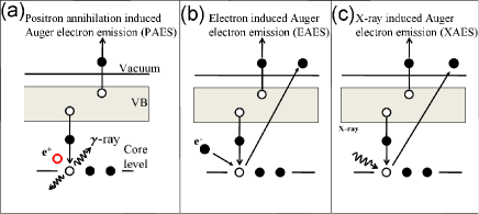
Based on these considerations, PAES spectra can be understood and analyzed based on just two factors- the usual Auger peak (C-VV transition) and the intrinsic loss(C-VVV transition)ramaker:1614 [C=Core, V= Valence]. The intrinsic loss associated with creation of a core hole has mostly been studied in context of the asymmetricity in the photopeak and presence of intrinsic plasmons in X-ray photoelectron spectroscopy (XPS) and is refered to as Mahan-Nozieres-DeDominicis effect MahanExcitons ; NozieresSingularities ; DoniachSingularitiesXPS ; tougaard1988quantitative ; HufnerXPS . The intrinsic loss reflects as a tail on the low energy side of the core peak and is assumed to extend to below the peak tougaard1988quantitative . The distinction between intrinsic and extrinsic electrons is based on the observation that the latter were related to electron transport in the solid while the former were due to creation of the core hole. Since the creation of core hole and the associated Auger process are essentially a single step process JensenLineNarrowing similar assymetricities should be present in Auger peaks as well. Experimental verification of this has been attempted solely by Auger-photoelectron coincidence spectroscopy (APECS) where a clear distinction between extrinsic and intrinsic electrons cannot be madeJensenAPECS ; ThurgateIntrinsic ; VanRiessenDPE . Hence an exact quantitative and qualitative prediction over the whole energy range has been missing. In PAES the core hole creation probability is independent of the incident positron energy which allows us to set the incident positron energy ( eV) well below the secondary electron creation threshold. The resultant spectra show a low energy tail (LET) JensenAPECS with intensity () times that of the Auger peak intensity () for Cu(Au) at energies below the Auger energy and extending to eV. The LET has been interpreted as arising mostly from intrinsic loss associated with the creation of the core hole. The spectral weight of intrinsic part of the LET is times that of the Auger peak area which has been concluded as evidence of multi electron emission once the core hole is created. This process is analogous to the double Auger process in noble gases PhysRevLett.14.390 and similar to photon induced correlated electron emission from solids PhysRevLett.89.086402 . The results have been interpreted as signature of electron correlation in the valence band JensenAPECS ; VanRiessenDPE .
II Experimental
The experiments were carried out in the time of flight -positron annihilation induced Auger electron spectrometer (tof-PAES) xie2002positron which uses a magnetic bottle analyzer JPhysESciIns.16.313 . Positrons emitted via beta decay from a mCi source were moderated using a polycrystalline Tungsten (W). The upper limit on the positron beam energy, , is given by the following equation
| (1) |
where is the positron work function of the moderator( eV for W), and are the bias on the moderator and sample with respect to the ground and is the electronic charge. The low energy positrons are guided to the sample, located m away, using fields. The whole spectrometer is housed in Helmholtz cage to cancel out the earth’s magnetic field. The energy of the outgoing electron is referred to the vacuum level.
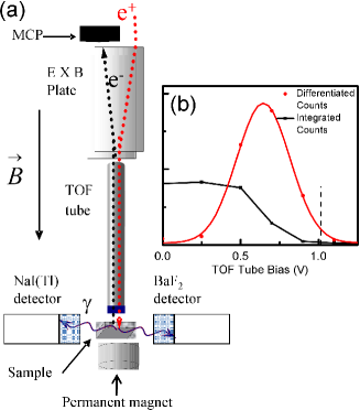
The annihilation gamma rays are detected by BaF2 and NaI detectors as shown in Fig. 2a. The outgoing electrons from the sample are parallelized using the divergent field of a permanent magnet. The electrons then fly down a retarding time of flight tube (tof tube) and are detected by a Micro channel plate (MCP). The MCP signal is used as the START while the delayed BaF2 signal provides the STOP (reverse timing) of the Time to Amplitude convertor (TAC). The TOF-PAES spectra are obtained by histogramming the output of the TAC. A calibration procedures detailed in reference Mukherjee2010AMS was used to determine the relation between the measured time of flight and the kinetic energy of the electrons leaving the sample. To estimate the contribution of accidental coincidence to tof-PAES spectra, a second setup referred to as the triple coincidence setup was used which takes advantage of the fact the annihilating gamma rays are emitted at an angle of with respect to each other. In this the STOP signal is the coincidence detection of the collinear keV gamma rays by BaF2 and NaI(Tl). The triple coincidence set up, by requiring the detection of two almost antiparallel gamma rays, was designed to discriminate against events in which one or both of the annihilation gamma rays generate secondary electrons as a result of Compton scattering in the sample or surrounding chamber walls.
The mT transport field used in the TOF spectrometer is particularly well suited for efficiently transporting the low energy positron (which was incident at eV at the sample) as well as the low energy electrons emitted from the sample. A volt sample bias was used to boost the kinetic energy of electrons emitted from the surface permitting measurements of electrons emitted from the surface all the way down to eV. The time of flight for a eV electron (corresponding to eV KE emission from the sample) was which was well within the measuring range of the spectrometer.
The incident beam profile (shown in Fig. 2(b))at eV sample bias was fitted with a Gaussian of eV FWHM and maximum at eV. % of the positrons have energy less than eV and this is referred to as the beam energy. This beam energy was used to obtain the Auger spectra of Cu and Au. During the measurements of the Auger spectra, the sample was biased at V with respect to the TOF drift tube.
An Au sample (a % pure polycrystalline foil, mm thickness) was sputter cleaned every hours while a Cu(100) sample (a % pure, mm diameter mm thickness) was sputter cleaned followed by annealing at oC every hours. The PAES spectrum was used to monitor the cleanliness of the sample and no significant contamination of the surface was found in the period between two sputtering times.
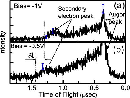
The sensitivity of PAES to the low energy electrons ( eV) is demonstrated in spectra shown in Fig. 3 which were obtained with an incident beam energy of eV. The incident positron energy was changed by varying the moderator bias (Eq 1) while keeping the electric and magnetic fields between the sample and MCP same. The peaks in the timing spectra (Fig. 3) are the Auger peak and the positron sticking induced secondary electron peak Mukherjee2010AMS . The lagging edge of the secondary electron peak (corresponding to the longest flight times) moves to shorter flight time as the sample bias is increased from V to V. These results confirm the ability of the tof-PAES system to detect and measure the energy of electrons emitted from the sample down to sub-eV energies. To obtain the Auger spectra, the moderator voltage was changed back to get a eV beam incident on the sample at V bias. All the Auger spectra were taken with this setting and sample bias V.
III Result and Discussion
The PAES spectra from Cu and Au are shown in Fig. 4. The Auger peaks in the case of Cu and Au are and respectively. The LET can be seen to extend from eV for Cu and eV for Au. The argument that the LET is due to the Auger electrons only can be ruled out by noting that secondary electron yield () will be for Cu(Au) while the maximum value of for most metals is Joy2005electronYield . Unlike earlier study of Cu Auger peaks Chiarello1993MVVCu , we did not observe any plasmon peaks on the low energy side of the Auger peak which is consistent with other PAES studies Zhou1996positron ; Hugenschmidt2010PAES .
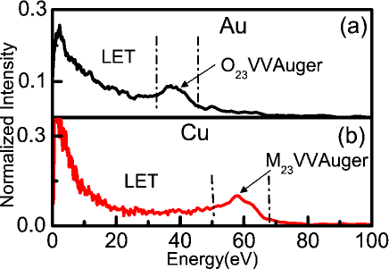
LET associated with the Auger peak has been earlier studied by Auger-photoelectron coincidence spectroscopy (APECS) JensenAPECS ; ThurgateIntrinsic and PAES Zhou1996positron . Both the studies were limited in the energy range studied ( eV for APECS and eV for PAES). The APECS spectra were further limited as the signal was an average over several atomic layer () and a background due to true coincidences involving inelastically scattered photo electrons from the valence band. Earlier PAES experiments employed a positron beam of eV and hence the low energy part of such spectra were dominated by extrinsic electrons. In the experiments reported here, the Auger signal comes from the topmost layer of the atoms Weiss1988PAES and the primary beam induced secondary electrons are energetically forbidden. Hence the PAES spectrum should contain the major spectral weight in the allowed Auger transition energy region, , where is binding energy of the core electron, is the width of the valence band and E is the energy of the electron. In our experiments, we find that majority of the intensity is in LET region (Fig. 4).
Following the argument of Ref. JensenAPECS, ; ThurgateIntrinsic, , the LET intensity associated with the Auger peak can be broken down to intrinsic and extrinsic contributions
| (2) |
where is the spectrum in LET region and the factors on the right side of the equation are the intrinsic and extrinsic contributions to it. The extrinsic part, in a usual Auger spectrum, is caused by primary beam and the transport of the Auger electrons through the solid. As suggested in Ref. Sickafus1977SecE2, ; SickafusSecE1, , the extrinsic part can be broken down into two components
| (3) |
where is the primary beam induced secondary electron spectrum, is the spectrum due to the Auger electron scattering inelastically with surface and subsurface atomsSickafus1977SecE2 . The area under the Auger peak in PAES spectrum ( eV for Cu and eV for Au) is refered to as . The inherent assumption in these analysis is that creation of Auger electrons and their subsequent emission can be treated separately werner2001three .
As discussed above, we used an incident beam whose energy was below the threshold energy that could cause secondary electron emission. It has been demonstrated in Ref. Mukherjee2010AMS, that the threshold for positron induced secondary electron emission is given by:
| (4) |
where is the maximum energy of emitted electron, is the electron work function and is the binding energy of the positron in in the image potential well Mukherjee2010AMS . For Cu(Au), eV knights1996effect ; *Farjam1987positronPHIand eV and hence the threshold for secondary electron emission is eV. The Auger spectra shown in Fig. 4 were obtained with an incident beam whose kinetic energy on the sample surface was eV thus making the beam induced secondary electron emission channel energetically forbidden.
Earlier studies Mayer1990PAES ; *Soininen1991PAES have shown that backgrounds due to positron annihilation-gamma ray induced secondary electrons were not significant in the PAES measurements. These experiments showed that it was possible to turn off the positron annihilation induced Auger signal by thermally desorbing the positrons form the surface state into the vacuum as positronium Ps (a hydrogen like atom composed of an electron and positron). Most of the Ps annihilate in close proximity to the sample. Consequently if gamma ray induced secondary electrons were a significant source of background signal, that signal should still be present even after the positrons are desorbed from the surface state as Ps. The data in Fig. 5(a) show the results of experiments, which are similar to Ref. Mayer1990PAES, ; *Soininen1991PAES. The average count of the high temperature spectrum() are only of the RT count rates (obtained after cooling the sample to room temperature). This provides an upper bound on the gamma induced secondary background of of the observed signal from the LET and demonstrates that gamma induced secondaries are not an important source of background in our measurements. The fact that the signal returned after the sample is cooled demonstrates that heating the sample did not produce significant contamination of the surface.
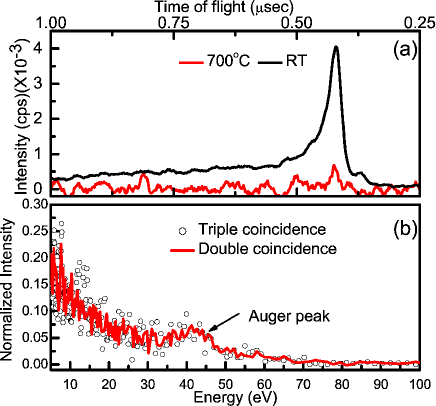
Further verification of the absence of this channel is done by comparing the PAES signal to the triple coincidence setup described above. In the latter, a measured coincidence between the two annihilation gamma rays, emitted at angle to each other, was required in order to produce a valid STOP signal to the TAC. The triple coincidence measurement insured that the annihilation events were taking place at the sample since two gamma annihilation taking place at some distance from the sample would not be in the simultaneous view of both detectors. The requirement of triple coincidence would strongly suppress background due to annihilation induced secondary electrons generated on surfaces other than the sample. The triple coincidence set-up will also strongly suppress events where one of the gamma rays undergoes Compton scattering or photo emission in the sample. The PAES and the triple coincidence spectrum from Au are shown in Fig. 5(b). The LET region ( eV) can be seen to have similar intensity in both the PAES and triple coincidence spectra (the poorer statistics of the triple coincidence measurements are a consequence of the low count rate associated with the reduced joint detection efficiency of the two gamma detectors) proving that the gamma induced background has negligible contribution in LET.
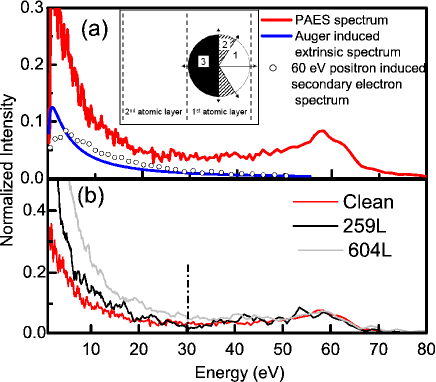
Next, the extrinsic contribution to the LET by the Auger electrons undergoing scattering in the surface and subsurface region is explored. The inset in Fig. 6(a) represents an isotropic source of Auger electrons in the topmost atomic layer Sickafus1977SecE2 . The electron source is confined to the first atomic layer because of the high surface selective nature of PAES. The emitted electrons are divided amongst three types based on their probability of undergoing inelastic scattering. Region corresponds to the Auger electrons that escape the solid without suffering any inelastic or elastic collision and are eventually detected. These electrons show up as the peak in the Auger spectrum. Not all the electrons emitted in the forward direction will fall in this category. The ratio of such electrons to all Auger electrons emitted in forward direction is referred to as transmission probability (T). Region corresponds to those electrons which are emitted at a fairly large angle to the surface normal and hence will scatter inelastically with the selvedge layer. The ratio of such electrons to the total auger electrons in forward direction is given by . As discussed below, these electrons have shown to be contributing mostly to the cascade region ( eV for Cu). Region corresponds to the Auger electrons that are emitted towards the subsurface region and are assumed to be completely lost in the cascade process. Since isotropic nature of Auger emission is assumed, the number of electrons in region will be the equal to the sum of those in region and . The transmission factor, T, has been calculated using the Beer lamberts cosine law and is written as mehl1990investigation
| (5) |
where is the inelastic mean free path of the Auger electron from Cu(Au) NISTinelastic , is the distance the electrons travel in the solid (Å), is the angle from the surface normal and is the azimuthal angle. Hence, T= has been calculated for Cu-(Au-) Auger electron. The PAES spectra from Cu surface with different coverage of residual gases is shown in Fig. 6(b). It can be noticed that the major affect of altering the surface roughness or chemistry is in the low energy part of the LET ( eV for Cu). This leads us to conclude that the Auger electrons from region 2 (Fig. 6(a)) contribute mostly to the cascade region of the LET. The secondary electron spectrum produced by inelastic scattering of the Auger electrons (represented by 2 and 3) has been modeled as suggested by Ref. Seah1969132, and is expressed as , where is the intensity of the secondary electron spectrum, is the energy of the electron, is the energy of the primary beam, is the work function of the metal and m is a constant. In our case , is taken as the Auger peak energy and is eV for Cu- and eV for Au- transition. This abovementioned line shape is for a beam energy of and eV normally incident on a polycrystalline copper surface while the electrons emitted from one specific angle is detected. This is in contrast to tof-PAES where the spectra are angle integrated. Hence, for the sake of comparison, we have measured the eV positron induced secondary electron spectrum from Cu surface using tof-PAES (Fig. 6(a)). Here we have used the result that positron and electron induced secondary electron yields tend to be similar Weiss1989PosSecE . It can be seen that the shape of the positron induced and theoretical secondary electron spectrum are quite similar providing extra confidence in modeling the Auger induced secondary electron spectrum by the form mentioned by Ref. Seah1969132, . The area under the secondary electron curve (Fig.6(a)) has been normalized such as to yield a Joy2005electronYield for Cu (Au) with a primary beam intensity of . Here, refers to the area under the Auger peak ( eV for Cu and eV for Au) while he first term in the bracket refers to the electrons from the region and the last term refers to electrons from region . Thus the spectral weight of the extrinsic part can be written as , where represents the upper limit of LET ( eV for Cu(Au)).
Representing the integrated terms by the respective intensity terms ( ) and dividing both sides by the Auger peak area () ,
| (6) |
Substituting the values Cu(Au) ( and ), the ratio of the intrinsic part of the LET to the Auger peak area ( ) for Cu(Au) is .
The Cu- and Au- Auger transition with the estimated extrinsic contribution subtracted is shown in Fig. 7. The ratio of spectral weight in the main Auger peak to the intrinsic LET region is . The intrinsic LET can be interpreted as due to the core holes decaying via multi electron emission process and is referred to as C-VVV processramaker:1614 . The intrinsic emission is mostly thought of in terms of sudden limit which means that the core hole was created in a timeframe less than that of the Auger lifetime () HimpselAdiabaticAuger1980 . If the time taken to create the core hole is less then the Auger lifetime then the process is termed adiabatic Darrahadiabatic1984 . Adiabatic process is evident mostly in resonant emission as the outgoing photoelectron has small velocity so that the valence electrons, effectively, see no change in the effective charge. To establish the timescale in which the core hole is created in PAES, we have to consider the time taken by the positron to tunnel into the core region ( ps) FertigTunnelingtime1990 ; *SteinbergTunnelingtime1990; *ChuprikovTunneling2006-1; *ChuprikovTunneling2006-2; Mills . Hence the valence electrons see some effective charge, say Z, which changes slowly () from as the positron tunnels into the core region. This is followed by rapid annihilation ( sec)Mills while the effective charge seen by the valence electrons remains at . Hence the PAES process can be considered to be in adiabatic regime and here we show that such emissions are possible in adiabatic regime as well.
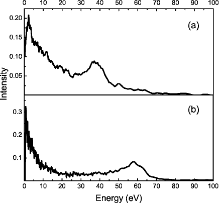
The spectrum in Fig. 7 has been used to calculate the probability of core holes decaying via C-VVV process. Since such a process entails emission of two electrons (sharing the energy of the usual Auger electron), the spectral weight of the C-VVV process will be twice that of the conventional CVV process. Hence the percentage of core holes decaying via multi electron emission for Cu(Au) has been calculated to be . The C-VVV emission probability has also been used to calculate the positron-core electron annihilation probability at surfaces. Earlier calculations PhysRevB.41.3928 considered only the the core-holes which decayed via the CVV process. Hence a and core annihilation probability was calculated for Cu() and Au(). Based on our experiments, we find the respective annihilation probability would be and which compares well with recent theoretical estimate fazleev2010oxidation ; AlataloCoreannProb1996 .
IV Conclusion
We have reported the first background free measurement of the complete spectra of low energy electrons emitted as a result of Auger transition in metals. By depositing low energy () positrons directly into the surface state Mukherjee2010AMS it was possible to excite Auger transitions from atoms at the surface without generating any primary beam induced secondary electrons. Localization of the positrons in the surface state ensures that almost all of Auger transitions occur in the topmost atomic layer. The resultant spectra showed that majority of the spectral weight is in the low energy tail associated with the Auger peak and extends to eV. Estimates based upon measurements of the electron induced secondary electron yield and inelastic scattering probability of electrons with selvedge indicate that extrinsic contributions account for less than of the LET in case of Cu(Au). Our results suggest that the intrinsic part of LET is due to the process in which the core hole decays by emission of more than one Auger electron (C-VVV). Assuming that the intrinsic process involves emission of only two electrons, it has been calculated that of the core holes in Cu(Au) decay via multi electron emission. This result was used to obtain new estimate of positron-core electron annihilation probability for Cu and Au which agree well with theoretical calculations. Since in the case of multi electron Auger emission, the valence electrons are emitted simultaneously, our studies are analogous to spectroscopy of photon induced emission of electron pairs PhysRevLett.89.086402 and provide another way of probing electron correlation effects in valence band of metals. Our results also have important implications in quantitative analysis of Auger spectraseah1996quantitative . In particular, we show that a significant fraction of core holes decay via multiple electron processes. These processes result in a decrease in the Auger peak intensity that is not fully accounted for in the usual Beer-Lambert based calculations of the escape probability. Consequently, estimates based upon measuring of the integrated intensity in the Auger peak region alone may lead to an underestimate of the number of initial core hole excitations. This has important implication for the use of PAES in estimating core hole annihilation probabilities fazleev2010oxidation and for the use of Auger spectroscopy in the quantitative analysis of surfaces.
V Acknowledgement
We wish to acknowledge useful discussion with D. E. Ramaker, J.Moxom and A.G.Hathaway. This work was supported by the Welch Foundation, Y1100 and NSF Grant No..
References
- (1) D. E. Ramaker, Journal of Vacuum Science & Technology A Vacuum, Surfaces, and Films 7, 1614 (1989)
- (2) W. S. M. Werner, W. Smekal, H. Störi, H. Winter, G. Stefani, A. Ruocco, F. Offi, R. Gotter, A. Morgante, and F. Tommasini, Phys. Rev. Lett. 94, 038302 (Jan 2005)
- (3) M. I. Trioni, S. Caravati, G. P. Brivio, L. Floreano, F. Bruno, and A. Morgante, Phys. Rev. Lett. 93, 206802 (Nov 2004)
- (4) S. Tougaard, Surface and Interface Analysis 11, 453 (1988)
- (5) M. Seah, Surface Science 32, 703 (1972)
- (6) M. Seah, Surface Science 17, 132 (1969)
- (7) E. N. Sickafus, Phys. Rev. B 16, 1448 (Aug 1977)
- (8) E. N. Sickafus, Phys. Rev. B 16, 1436 (Aug 1977)
- (9) M. Seah, Surface and Interface Analysis 24, 830 (1996)
- (10) V. Contini, C. Presilla, and F. Sacchetti, Surface Science 210, 520 (1989)
- (11) D. Ramaker, J. Murday, and N. Turner, Journal of Electron Spectroscopy and Related Phenomena 17, 45 (1979)
- (12) S. Mukherjee, M. P. Nadesalingam, P. Guagliardo, A. D. Sergeant, B. Barbiellini, J. F. Williams, N. G. Fazleev, and A. H. Weiss, Phys. Rev. Lett. 104, 247403 (June 2010)
- (13) K. O. Jensen and A. Weiss, Phys. Rev. B 41, 3928 (March 1990)
- (14) G. D. Mahan, Phys. Rev. 163, 612 (Nov 1967)
- (15) P. Nozières and C. T. De Dominicis, Phys. Rev. 178, 1097 (Feb 1969)
- (16) S. Doniach and M. Sunjic, J. Phys. C: Solida State Phys. 3, 285 (1970)
- (17) S. Hufner, “Photoelectron spectroscopy,” (Springer, 1994) pp. 112–119
- (18) E. Jensen, R. A. Bartynski, S. L. Hulbert, E. D. Johnson, and R. Garrett, Phys. Rev. Lett. 62, 71 (Jan 1989)
- (19) E. Jensen, R. A. Bartynski, R. F. Garrett, S. L. Hulbert, E. D. Johnson, and C.-C. Kao, Phys. Rev. B 45, 13636 (Jun 1992)
- (20) C. P. Lund, S. M. Thurgate, and A. B. Wedding, Phys. Rev. B 49, 11352 (Apr 1994)
- (21) G. v. Riessen, Z. Wei, R. S. Dhaka, C. Winkler, F. O. Schumann, and J. Kirschner, Journal of Physics: Condensed Matter 22, 1 (Feb 2010)
- (22) T. A. Carlson and M. O. Krause, Phys. Rev. Lett. 14, 390 (Mar 1965)
- (23) N. Fominykh, J. Berakdar, J. Henk, and P. Bruno, Phys. Rev. Lett. 89, 086402 (Aug 2002)
- (24) S. Xie, Positron annihilation induced Auger electron spectroscopy of inner shell transitions using the time-of-flight technique, Ph.D. thesis, University of Texas at Arlington (2002)
- (25) P. Kruit and F. H. Read, Journal of Physics E: Scientific Instruments 16, 313 (1983)
- (26) Y. Lin and D. C. Joy, Surface and Interface Analysis 37, 895 (2005)
- (27) G. Chiarello, A. Amoddeo, R. G. Agostino, L. S. Caputi, and E. Colavita, Phys. Rev. B 48, 7779 (Sep 1993)
- (28) H. Zhou, Auger Line Shape Measurements Using High Resolution Positron Annihilation Induced Auger Electron Spectroscopy, Ph.D. thesis, University of Texas at Arlington (1996)
- (29) C. Hugenschmidt, J. Mayer, and K. Schreckenbach, Journal of Physics: Conference Series 225, 012015 (2010)
- (30) A. Weiss, R. Mayer, M. Jibaly, C. Lei, D. Mehl, and K. G. Lynn, Phys. Rev. Lett. 61, 2245 (Nov 1988)
- (31) W. Werner, H. Tratnik, J. Brenner, and H. Störi, Surface Science 495, 107 (2001)
- (32) A. Knights and P. Coleman, Surface Science 367, 238 (1996)
- (33) M. Farjam and H. B. Shore, Phys. Rev. B 36, 5089 (Oct 1987)
- (34) R. Mayer, A. Schwab, and A. Weiss, Phys. Rev. B 42, 1881 (Aug 1990)
- (35) E. Soininen, A. Schwab, and K. G. Lynn, Phys. Rev. B 43, 10051 (May 1991)
- (36) D. Mehl, Investigation of the surface sensitivity of positron-annihilation- induced auger-electron spectroscopy, Ph.D. thesis, University of Texas at Arlington (1990)
- (37) “NIST electron inelastic-mean-free-path database,” http://srdata.nist.gov/xps/ (2010)
- (38) R. Mayer, E. Gramsch, and A. Weiss, Phys. Rev. B 40, 11287 (Dec 1989)
- (39) T. D. Thomas, Phys. Rev. Lett. 52, 417 (Feb 1984)
- (40) H. A. Fertig, Phys. Rev. Lett. 65, 2321 (Nov 1990)
- (41) A. M. Steinberg, Phys. Rev. Lett. 74, 2405 (Mar 1995)
- (42) N. L. Chuprikov, Russian Physics journal 49, 119 (2006)
- (43) N. L. Chuprikov, Russian Physics journal 49, 314 (2006)
- (44) A. P. Mills, Jr., private communications (2010)
- (45) F. J. Himpsel, D. E. Eastman, and E. E. Koch, Phys. Rev. Lett. 44, 214 (Jan 1980)
- (46) N. Fazleev, M. Nadesalingam, W. Maddox, S. Mukherjee, K. Rajeshwar, and A. Weiss, Surface Science 604, 32 (2010)
- (47) M. Alatalo, B. Barbiellini, M. Hakala, H. Kauppinen, T. Korhonen, M. J. Puska, K. Saarinen, P. Hautojärvi, and R. M. Nieminen, Phys. Rev. B 54, 2397 (Jul 1996)