Effect of strain on the thermoelectric properties of silicon: An ab initio study
Abstract
On the basis of detailed first-principles calculations the anisotropic thermoelectric transport properties of biaxially strained silicon were studied with focus on a possible enhancement of the powerfactor. Electron as well as hole doping were examined in a broad doping and temperature range. In the low-temperature and low-doping regime an enhancement of the powerfactor was obtained for compressive and tensile strain in the electron-doped case and for compressive strain in the hole-doped case. In the thermoelectrically more important high-temperature and high- doping regime a slight enhancement of the powerfactor was only found for the hole-doped case under small biaxial tensile strain. The results are discussed in terms of band-structure effects. An analytical model is presented to understand the fact that the thermopower decreases if degenerate bands are energetically lifted due to a strain- induced redistribution of states.
pacs:
31.15.A-,71.15.Mb,72.20.Pa,72.20.-i1 Introduction
Thermoelectrics convert heat into electric current, and vice versa. Known for more than 60 years, thermoelectrics attract currently attention [1, 2, 3, 4]. With nearly 90 per cent of the worlds power being generated by low efficient heat engines, thermoelectric modules could potentially convert parts of this wasted heat into electricity. Their conversion efficiency can be stated by the figure of merit
| (1) |
where is the electrical conductivity, the thermopower, and are the electronic and phononic contribution to the thermal conductivity, respectively. The numerator of Eq. 1 is called powerfactor .
While was challenging to be reached in the last decades, nowadays nanostructured thermoelectrics enable even larger values of [5, 6, 7]. Unfortunately, those materials are often based on environmentally unfriendly lead, tellurium or selenium compounds and are therefore hard to integrate in semiconductor electronics.
Silicon, the cradle of modern semiconductor electronics, is nonpolluting, readily available, cheap and perfectly integrated in present electronics infrastructure. While silicon has been stated as inefficient thermoelectric in the past due to his enormous thermal conductivity [8], recent experiments and theory revealed that nanostructuring could lead to thermoelectric efficiencies comparable to state of the art commercial thermoelectric materials [9, 10, 11, 12, 13].
As in nanostructured materials mechanical strain plays an important role, this paper will focus on the influence of biaxial strain on the electronic thermoelectric transport properties of bulk silicon , which might occur in rolled up and layered Si heterostructures [14, 15, 16, 17]. It is well known, that similar strain physics, e.g. band splitting and band deformation are expected for strained three dimensional systems, as well as for one and two dimensional silicon devices in complex strain states. A comprehensive overview on this can be found in ref. [14]. In detail these common strain physics affect the electronic carrier transport depending on the dimensionality, temperature and doping density. The question to be answered in this paper will be whether tensile or compressive strain will lead to an enhancement or reduction of the powerfactor in silicon under a certain doping and temperature environment. Beside our interest in the high temperature thermoelectric application of strained silicon we want to emphasize the possible importance of our results in the low temperature regime for the metal-oxide-semiconductor device community, where the knowledge of the thermoelectric properties of silicon under strain could help to understand parasitic effects in these devices. In the low doping regime at low temperature, an enhancement of one part of the powerfactor, namely the electrical conductivity, under externally applied strain was found and heavily investigated in the last decades.[18, 19, 14] For this purpose the paper will be organized as follows. In section 2 we introduce our first principle electronic structure calculations based on density functional theory and the transport calculations based on the solution of the linearized Boltzmann equation. With this knowledge we start the discussion of the thermoelectric transport properties of unstrained bulk silicon (Sec. 3.1) and present afterwards the influence of biaxial strain on the electron or hole doped case of silicon in section 3.2. In the last paragraphs 3.3 and 4 the optimal powerfactor under strain due to variation of doping is determined and analyzed, while estimations of the possible figure of merit are given.
2 Methodology
Our approach is based on two ingredients: first principles density functional theory calculations (DFT), as implemented in the QuantumEspresso package [20] and an in-house developed Boltzmann transport code [21] to calculate the thermoelectric transport properties.
2.1 Electronic structure
In a first step the band structure of the strained and unstrained Si was calculated using the general gradient approximation (GGA) and the PBE exchange correlation functional [22]. Fully relativistic and norm-conserving pseudo potentials [23] were used to treat the spin-orbit splitting of the Si valence bands in a correct way. The calculations were performed with the experimental lattice constant for a face-centered tetragonal eight atom unit cell. The in-plane biaxial strain is simulated by changing the ratio but keeping the cell volume constant. Throughout the paper the biaxial strain will be given in units of the relative change of the in-plane lattice constant as . That means tensile strain considers changes , while compressive strain means .
As expected, our DFT calculations underestimate the size of the band gap at zero temperature and do not reproduce the temperature dependence of the gap. For this purpose we included a temperature-dependent scissor operator [24], so that the strain- and temperature-dependent energy gap in eV becomes
where is the zero temperature gap obtained by our self-consistent DFT calculations, is a static correction to fulfill the experimental low temperature gap. The third part of equation 2.1 is the correction of the temperature dependence of the band gap [25] in a wide temperature range with T given in K.
2.2 Boltzmann transport
With the converged results from the first step we are now able to obtain the thermoelectric transport properties by solving the linearized Boltzmann equation in relaxation time approximation (RTA) [21]. Boltzmann transport calculations for thermoelectrics have been carried out for quite a long time and show reliable results for metals [26, 27, 28, 29] as well as for wide- and narrow gap semiconductors [30, 31, 32, 33]. Within in here the relaxation time is assumed to be constant with respect to wave vector k and energy on the scale of . This assumption is widely used for metals and doped semiconductors. The constant relaxation time is a big advantage for the calculation of the thermopower without any adjustable parameter, while lacking any doping or temperature dependence of . For unstrained silicon, doping dependent relaxation times in the order of 15-150 fs for electron doping and 6-65 fs for hole doping could be estimated from experiments in ref. [34]. To concentrate on the bandstructure effects we assume the relaxation time does not depend on strain, while it was shown, that under strain the dominant scattering process varies: For unstrained Si, the room-temperature scattering is dominated by optical phonons, i.e., intervalley scattering, whereas for strained Si, this scattering process is less efficient [35, 36].
The temperature- and doping-dependent thermopower in- and cross-plane is defined as
| (3) |
where
| (4) |
is the transport distribution function as termed by Mahan and Sofo [37], for given chemical potential at temperature and carrier concentration determined by an integration over the density of states
| (5) |
where is the conduction band minimum and is the valence band maximum. As can be seen straight forward from eqs. 3 and 4 the electrical conductivity is then given by
| (6) |
The Fermi-surface integration, which is requested in equation 4, is performed within an extended tetrahedron method [38, 39, 40] interpolating the calculated Eigenvalues on a mesh of at least 13950 k points in the irreducible part of the Brillouin zone. was determined on a fine energy mesh with a step width of . Convergence tests confirmed that the calculation of the electrical conductivity and the thermopower at a given temperature via equations 6 and 3 requires for a quite large range. Convergence of the integrals 4 and 5 was achieved with an adaptive integration method for in the limit of low carrier concentrations .
3 Thermoelectric transport
3.1 Unstrained case
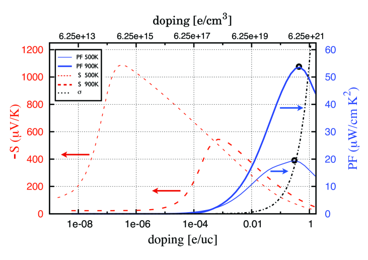
Since the thermoelectric transport properties of the strained silicon will always be discussed in comparison with the unstrained case, we will provide an insight into the transport properties of the unstrained silicon, first. In figure 1, the thermopower and the powerfactor are shown for two different temperatures (500K and 900K) in a wide doping range. The qualitative behavior of the electrical conductivity is indicated by the dashed-dotted line to emphasize the trend of the resulting powerfactor. The picture is well known for the interrelation of electronic transport and the thermoelectric properties of semiconductors [41, 1]. At constant temperature the thermopower (cf. red dashed lines in figure 1) decreases at very low and higher doping level and reaches a maximum inbetween [41].
As can be seen from figure 1 the thermopower reaches a maximum around an electron carrier concentration of at 500K, while the maximum at 900K is shifted to a larger doping level of . Beside that, the maximum of the more relevant powerfactor (cf. blue solid lines in figure 1, optimal values indicated by black open circles) is shifted to huge electron carrier concentrations of about . This is determined by the linear increase of the electrical conductivity with increasing charge carrier concentration. Obviously, there is not much space to optimize the powerfactor with respect to temperature and charge carrier concentration for unstrained silicon. We will focus on this optimization in more detail in subsection 3.3.
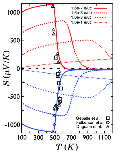
The complex dependence of the thermopower on temperature and doping is shown in figure 2 for electron and hole doped unstrained silicon at different doping concentrations. For low temperatures and doping levels the thermopower reaches values of and above, which is caused by the location of the chemical potential near the band edges. The denominator of equation 3, proportional to the electrical conductivity, is small, while the nominator is large, the thermopower gets maximal. At fixed charge carrier concentration the position of the chemical potential is shifted towards the middle of the gap with increasing temperature. The nominator in equation 3 decreases, because it is mainly determined by the opposite contributions of the tails of the derivative of the Fermi-Dirac distribution function with respect to the valence and conduction band (equation 4, n=1). At a distinct temperature of about the thermopower rapidly vanishes. At this temperature the electronic transport enters into the bipolar intrinsic regime. To emphasize the relevance of our calculations experimental results for merely pure silicon in the intrinsic transport regime are added in figure 2. We want to point out, that the thermopower does not vanish at all, but converges to small negative values for electron, as well as for hole doping. At large charge carrier concentrations of about (dotted lines in figure 2), where the powerfactor becomes large, the thermopower grows linearly with temperature upto values of at . In the heavy doped regime the chemical potential is located deeply in the bands and equation 3 qualitatively coincides with the well known Mott relation for the thermopower in RTA [45].
3.2 Optimization of the powerfactor by strain
3.2.1 Electron doping
Having provided a general view on the thermoelectric transport properties of unstrained silicon above, we will now focus on the effect of biaxial strain on those properties. The results are presented in comparison to the unstrained case, starting with the electron doped case, followed by the hole doped case in subsection 3.2.2.
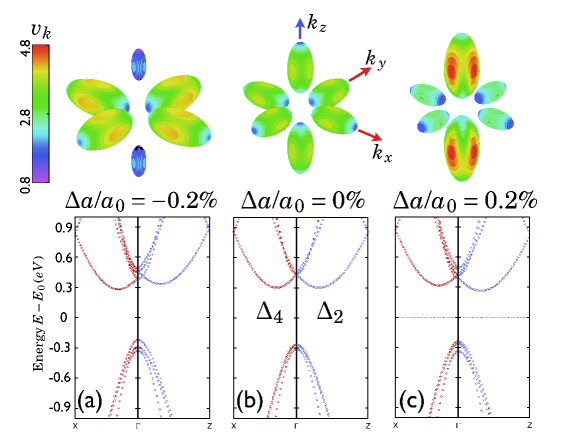
In strain-free bulk silicon, as introduced in section 3.1, the conduction-band minimum (CBM) consists of six equivalent valleys on the -X high symmetry line as shown in the middle panel of figure 3(b). The Fermi surface pockets corresponding to these valleys are shown on top, with the absolute value of the carriers group velocity, entering equation 4, plotted in color on the surface. The color code gives in units of . By applying biaxial in-plane strain, the six CBM valleys are energetically split into two groups. Four degenerate in-plane valleys and two degenerate cross-plane valleys (see figure 3 (a),(c)). While the number of electrons is fixed, the different sizes of the ellipsoidal pockets is caused by a change of occupation numbers under strain. The color code indicates the overall smaller Fermi velocities on the small pockets and in particular on the principal axis of the pockets, whereas larger velocities are found for states propagating perpendicular to the principal pocket axis.
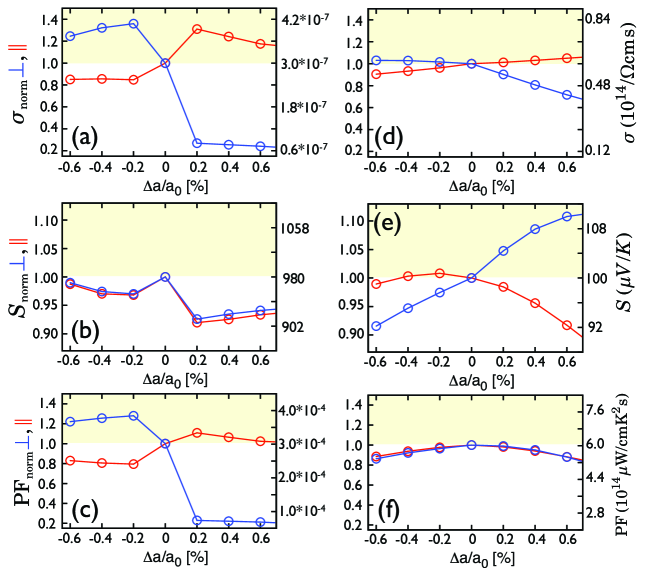
In figure 4 the thermoelectric transport properties of biaxial strained silicon for two fixed electron doping regimes are shown. First, we consider the left column (figures 4(a)-(c)), which shows the electrical conductivity , the thermopower and the resulting powerfactor for a low electron doping of and a low temperature of 100 K. For this doping and temperature value a large enhancement of up to 35% of the electrical conductivity is obtained for the in-plane component at low tensile strain and for the cross-plane component at small compressive strain. drops noticeable under small tensile strain up to 30% of the unstrained case, while experiences a slight drop down to 83% under small compressive strain, respectively.
With the conduction bands of silicon behaving parabolically near the band edges, the calculated transport properties can be understood for small charge carrier concentrations and low temperatures in terms of effective masses and occupation number redistributions (see [35]. With increasing tensile strain the bands lift up and the occupied states from the higher bands are transferred to the lowered bands (comp. figure 3(c)). At a certain tensile strain the pockets are completely depleted and solely the maximally occupied states contribute to the transport.
In simplified consideration one can estimate the relative change in the electronic conductivity from the relative change in the effective electron mass. As reported earlier [35] it is and , whereas the masses are in units of the free electron rest mass. For the in-plane component of the electrical conductivity at sufficient tensile strain only the lowered bands contribute with their perpendicular mass . With the notation
| (7) |
the normalized asymptotic value becomes:
| (8) |
For the in-plane component of the electrical conductivity at compressive strain only the four pockets of the lowered bands contribute equally with their parallel and perpendicular mass:
| (9) |
For the cross-plane conductivity at tensile strain it is
| (10) |
whereas at compressive strain becomes
| (11) |
Since the powerfactor is composed out of and we analyze the influence of strain on the thermopower as well. In the low temperature and doping regime (figure 4 left panel) no enhancement of thermopower at either compressive or tensile strain could be found. It can bee seen, that for tensile strain the thermopower decreases by about 10%, while for compressive strain a drop of about 5% is found. The difference between the in-plane and cross-plane thermopower is marginal. In terms of Motts formula [45] it means that the energy dependence of and is almost the same. Nevertheless it is interesting to understand why the thermopower of silicon is reduced under strain and why the decay changes for tensile and compressive strain.
For qualitative understanding of our ab initio results we apply a free electron model to discuss the thermopowers behavior on biaxial strain. The strain dependent electrical conductivity at zero temperature was modeled as proposed by [35] and then the thermopower was calculated by Motts relation in RTA [45]. Figure 5 shows the resulting thermopower under tensile and compressive strain for a small (dashed line) and a five times larger charge carrier concentration (solid line).
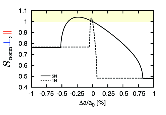
For small charge carrier concentration the thermopower rapidly drops to constant values of 48% for tensile and 76% for compressive strain, respectively. We note that the maximum of which is increased by 4% compared to the unstrained case is not located at zero strain and is shifted to very small values of compressive strain. This behavior is more pronounced for the large charge carrier concentration, where the maximum of the thermopower becomes wider and is shifted to values of -0.25% compressive strain. Again the enhancement reached for is about 4% and the asymptotic values keep unchanged with doping. We note that for the calculation of the thermopower the influence of the effective masses completely cancels. For this reason neither for the ab initio nor the analytic calculation a noticeable difference of the in-plane and cross-plane thermopower was found. The different saturation values of the thermopower under tensile and compressive strain again however can be explained in terms of a redistribution of electrons. For free electrons at T=0 the electrical conductivity and the resulting thermopower . The amount of charge carriers in one spin band is given by . With Motts relation . As stated before in this paper under sufficient tensile strain only the twofold degenerated pockets are occupied compared to the sixfold degenerated CBM pockets in the unstrained case, so the occupation of every pocket increases by a factor of 3. One directly yields . For compressive strain only the fourfold degenerated pockets contribute, so it is . The fact, that for larger charge carrier concentration larger strain has to be applied to reach these limits, is linked to the fact that higher strain is required to reach a complete redistribution of states into either the or pockets. As consequence of the discussed results we see in figure 4(c) an enhancement of the powerfactor in cross-plane direction up to 27% at small compressive strain, while the in-plane powerfactor is only marginally enhanced by about 5% under low tensile strain. In-plane transport under tensile strain at low doping and low temperature plays an important role in silicon based devices. Within figure 4(c) it is obvious that the strain induced influence of the powerfactor on this transport will play a minor role. We want to point out that the results on the thermopower discussed above are generally valid for all systems with degenerate occupied bands. Lifting of the degeneracy causes redistribution of electrons and reduction of the thermopower. While the low temperature and low doping case was convenient to provide some general findings on an analytical level, we will now focus on the high temperature and high doping regime (see figure 4 left panels) where the power factor might be suitable for thermoelectric application (see also 1). At a temperature of 900K the electronic bandstructure on a width of at least around the position of the chemical potential has to be included, which makes a description of the electronic transport properties within a spherical band picture impossible. Rather than providing analytical quantities a more qualitative description of our ab initio calculations will be given instead. The electrical conductivity in figure4(d) states the same qualitative tendencies for and as derived for the low temperature case. As a consequence of the high temperature and the related broadening of the Fermi-Dirac distribution in equations 4 and 5 as well as the high charge carrier concentration the redistribution of states as described before is not completed for the strain values considered here. The analytical limits for the enhancement of and for the given high doping and temperature should be achieved for biaxial strains of at least , respectively. It is worth mentioning, that the absolute value (cf. right scales in figures 4(a),(d)) of the electrical conductivity raised enormously compared to the low doping case as expected. As a consequence, the powerfactor rises absolutely but unfortunately no enhancement via strain was obtained. The strain-dependent behavior of the thermopower as shown in figure 4(e) compensates the behavior of the electrical conductivity. In the high doping-high temperature regime the thermopower shows a noticeable anisotropy between in-plane and cross-plane component. While the in-plane component confirms our analytical predictions for high doping (see black solid line in figure 5) and even shows the shifted maximum to compressive strain, the cross-plane component does not follow the analytical model. This might be explained by multiband effects and nonparabolic bands, with the latter being more relevant in the cross-plane direction. The overall resulting powerfactor summarized in figure 4(f) shows however no significant anisotropy. Furthermore no enhancement by biaxial strain could be obtained, in contrast a decrease of about 20% occurs.
3.2.2 Hole doping
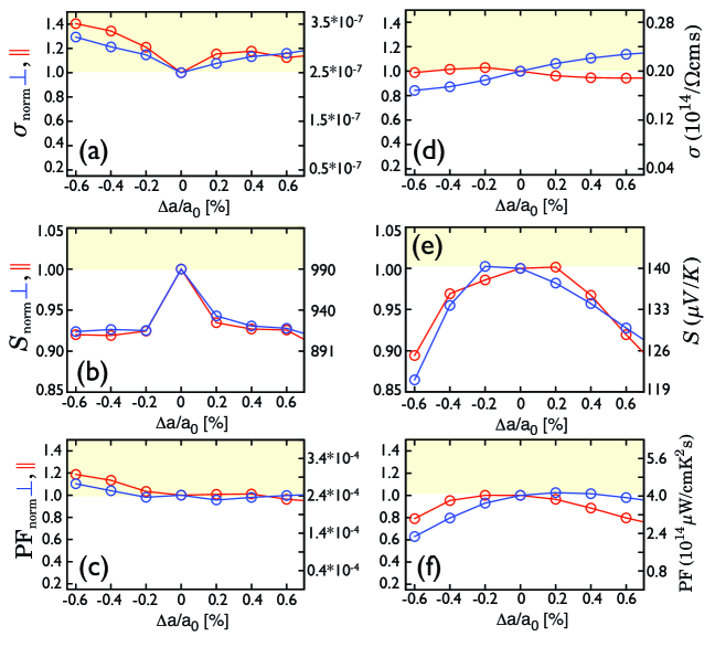
We will now focus in more detail on the thermolectric properties of hole doped biaxially strained silicon as presented in figure 6. Under full relativistic treatment the three valence bands next to the VBM at the -point are the heavy hole (HH), light hole (LH), and spin-orbit split-off (SO) hole. While the HH and LH are degenerate, the SO lies 44 meV apart (see figure 3 middle panel). Under biaxial tensile or compressive strain, the valence bands become highly anisotropic and a crossover between bands occurs so that they even loose their original meaning[46]. It was shown that mechanical deformation-induced changes in the band structure offers potential for significant enhancement of the hole mobility [47]. Nevertheless, a straightforward explanation of the ab initio calculations as done for the electron doped case is not any more possible. Actually tensile and compressive biaxial strain does not only cancel the degeneracy of the heavy and light hole bands, which will cause reduced intervalley phonon scattering, furthermore it also leads to a smaller effective conductivity mass and a further depletion of the uppermost hole band [14, 48]. Similarly to the electron doped case in figure 6 the thermoelectric transport properties for hole doped silicon under the influence of biaxial strain are shown for a fixed low doping, low temperature in figure 6(a)-(c) and fixed high doping, high temperature regime in figure 6(d)-(f). At low temperature and slight doping an increase of the electrical conductivity was found for tensile as well as for compressive strain for the in-plane component and the cross-plane component , while biaxial compressive strain tends to favor the enhancement of . As shown in figure 6(b) the thermopower for hole-doped silicon again experiences a drop of nearly 7% under compressive and tensile strain. A possible explanation for the almost symmetric drop of the thermopower under compressive and tensile strain might be again related to the number of bands being occupied. At small doping for compressive and for tensile biaxial strain the primarily occupied HH and LH split and only the upper hole band is depleted and dominates the character of the transport properties[14, 48]. Extending our analytical findings for the electron doped case one would expect, that . Through the counteracting behavior of electrical conductivity and thermopower under strain, again no enhancement of the powerfactor could be found (cf. figure 6(c)). Only under strong compressive biaxial strain a significant enhancement is visible in the low temperature/ low doping case. In the high doping and temperature regime not only the upper hole band plays an important role in transport, furthermore the former HH, LH and SO have to be mentioned. As shown in figure 6(d) an enhancement of around 10% compared to the unstrained case can be found for the cross-plane component under small tensile strain. For the in-plane electrical conductivity under compressive strain only a marginal influence on the strain can be reported. The thermopower shows a small anisotropy of the in-plane and cross-plane components. While the thermopower is mainly decreased for compressive or tensile strain, we again see a broadening of the thermopower drop in dependence on the applied strain with respect to the low doping regime. Beside the absolute values of the powerfactor being around 30% smaller than in the electron doped case (comp. figure 4(f) and 6(f)), a slight enhancement under thermoelectrically relevant doping and temperature conditions could be found for the cross-plane powerfactor under small tensile strain (see figure 6(f)).
3.3 Optimization of the powerfactor by doping
While up to this point the powerfactor and the incorporated thermoelectric transport properties were studied for fixed temperature and charge carrier concentration in dependence on the applied biaxial strain, we want to gain further insight in the doping dependence. Therefore the amount of charge carrier concentration to optimize the powerfactor and at given strain and fixed temperature of 900K was determined. This temperature seems to be a common temperature for thermoelectric application of silicon based devices. Figures 7 and 8 represent the results for the electron and hole doped case, respectively.
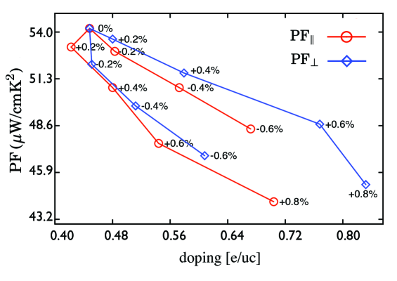
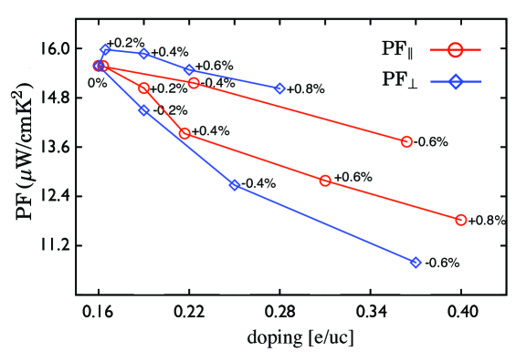
From figure 7 it becomes clear, that an enhancement of the powerfactor by sufficiently high electron doping can’t be stated. With increasing biaxial strain the in-plane and cross-plane thermopower decreases compared to the unstrained case. It is worth mentioning, that the charge carrier concentration has to be increased for increasing tensile and compressive biaxial strain to achieve the optimal powerfactor under the certain strain condition. Nevertheless, even for a raised optimal charge carrier concentration the powerfactor drops to about 80% of the value of the unstrained case for the largest strain values considered here. As an interesting fact one can see that under tensile strain the cross-plane powerfactor is always larger than the in-plane component , while under compressive strain it is the other way around and is smaller than . In contrast to heavily electron-doped silicon an enhancement of the powerfactor could be found for hole doped silicon, as shown in figure 8. Nevertheless, the enhancement is limited to the cross-plane contribution . Here we find an enhanced under small tensile strain of , while for tensile strain of 0.6% a value of the cross-plane powerfactor similar to the unstrained case is reached. We note, that the charge carrier concentrations, which are necessary to optimize the powerfactor in the hole doping case are about three times smaller than in the related electron doping case. Even though an enhancement of the cross-plane powerfactor under optimized hole doping and tensile strain can be found, unfortunately the absolute values of the powerfactor are sufficiently smaller than the absolute value of the and of electron-doped silicon under all strain condition examined here.
4 Tendencies on figure of merit
To evaluate tendencies of the figure of merit we are going to include and discuss experimental results for the lattice thermal conductivity , which adds up to our calculated electronic thermal conductivity for the total thermal conductivity . Involving the transport distribution function in eq. 4 the electronic contribution to the thermal conductivity is calculated as
| (12) |
For bulk silicon, porous silicon and thin films various temperature- and doping-dependent measurements are available [49, 50, 51, 12, 52]. It is well known, that the lattice thermal conductivity of silicon is strongly depends on temperature. While at room temperature a value of was reported, this value decreases to at and at [12, 50] making silicon an high temperature thermoelectric. Even at high temperatures and applicable doping the electronic contribution to the thermal conductivity is only a few percent of the total thermal conductivity. For bulk silicon it is reported, that the heat conduction is impeded by higher dopant concentrations [51]. Here the lattice thermal conductivity reduction due to the scattering by dopant ions overbalances the increase of the electronic thermal conductivity. Due to this behaviour the total thermal conductivity is weakly depends on doping for temperatures clearly above [49, 52]. Nevertheless, for nanostructured silicon, e.g. in silicon-based superlattices [11, 53] or nanoparticle bulk silicon [12], with a low lattice thermal conductivity of , it may occur that the electronic thermal conductivity contributes remarkably to the total thermal conductivity. At high doping levels above and temperature of the electronic contribution can be around and therefore approx. of the total thermal conductivity. While it was recently shown [54, 11], that tensile strain could lead to a reduction of the thermal conductivity by up to 15% in bulk silicon as well as in silicon thin films we did not include this in our estimation.
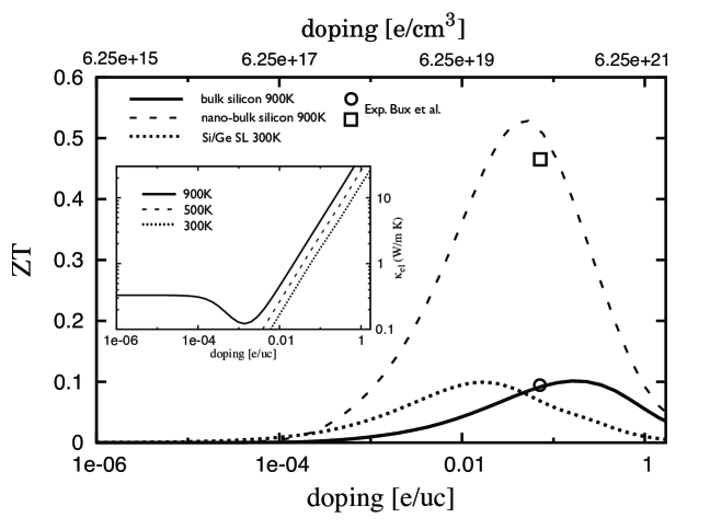
In figure 9(a) the doping dependent figure of merit for three silicon based systems is shown. We assumed doping independent experimental lattice thermal conductivities stated for high doping rates, to include the reduction of by ion scattering. Values of [12], [12] and [11] were used for single crystalline bulk silicon, nanostructured bulk silicon and a superlattice, respectively. Here we consider only electron doping, which appeared to be most promising. The calculated doping dependent electronic part is shown in the inset of fig. 9 for three different temperatures. For bulk silicon (solid line in fig. 9) we find a broad maximum for the figure of merit at 900K and high doping levels of , which is in good agreement to experiments by Bux et al. [12]. Compared to the related powerfactor (see fig. 1) the maximum shifts to lower doping concentrations due to the linear increase of at higher doping rates, and therefore a stronger decrease of ZT at high doping rates. If a reduction of the lattice thermal conductivity can be achieved by nano inclusions as reported in ref. [12] a remarkable of about at at 900K could be obtained making silicon an interesting high temperature thermoelectric (dashed line in fig. 9). Nevertheless, at room temperature the lowest thermal conductivities have been stated for silicon and germanium based superlattices [11, 53]. Therefore the dotted line fig. 9 estimates the figure of merit for a Si/Ge superlattice with a period of assuming no degradation of the electronic transport by the heterostructure. Here, at 300K, the maxium figure of merit is found around doping levels of with values of about , which are comparable to single crystalline silicon at 900K at ten times larger doping levels.
5 Conclusion
In conclusion, the thermoelectric transport properties of biaxially strained silicon were studied in detail with respect to a possible enhancement of the powerfactor. Two different doping and temperature regimes were analyzed in detail. A low doping () and low temperature regime (T=100K) suitable for metal-oxide-semiconductor device applications and a heavy doping () and high temperature regime (T=900K) suitable for silicon based thermoelectric modules.
It was shown that the electronic transport properties, namely the electrical conductivity and the thermopower are highly sensitive against strain. Nevertheless it was found that strain-induced effects in and compensate each other and no remarkable enhancement of the powerfactor by either compressive or tensile biaxial strain can be reached. On the other hand a reduction of the powerfactor of upto 20% (30%) under electron (hole) doping due to the influence of strain was found. The latter was assigned to a large extent to band-structure related redistribution of electrons. Estimations for the figure of merit under electron doping are given.
As a general result we showed that when degenerate VBM or CBM exist the thermopower decreases with deformation due to a redistribution of electrons in energetically lifted valleys. This could be the general explanation of the reduction of the electronic thermoelectric properties in strain-influenced heterostructures.
References
References
- [1] GJ Snyder and ES Toberer. Complex thermoelectric materials. Nature Materials, 7(2):105–114, 2008.
- [2] BC Sales. Thermoelectric materials: Smaller is cooler. Science, 295(5558):1248, 2002.
- [3] A Majumdar. Thermoelectricity in semiconductor nanostructures. Science, 303(5659):777, 2004.
- [4] H Böttner, G Chen, and R Venkatasubramanian. Aspects of thin-film superlattice thermoelectric materials. MRS bulletin, 31:211, Jan 2006.
- [5] R Venkatasubramanian, E Siivola, and T Colpitts. Thin-film thermoelectric devices with high room-temperature figures of merit. Nature, 413:597, Jan 2001.
- [6] T Harman, P Taylor, M Walsh, and B LaForge. Quantum dot superlattice thermoelectric materials and devices. Science, 297:2229, Jan 2002.
- [7] M Dresselhaus, G Chen, M Tang, and R Yang. New directions for low-dimensional thermoelectric materials. Advanced Materials, 19:1, Jan 2007.
- [8] CB Vining. Materials science: Desperately seeking silicon. Nature, 451(7175):132–133, 2008.
- [9] A Hochbaum, R Chen, R Delgado, and W Liang. Enhanced thermoelectric performance of rough silicon nanowires. Nature, 451:163, Jan 2008.
- [10] AI Boukai, Y Bunimovich, J Tahir-Kheli, JK Yu, WA Goddard Iii, and JR Heath. Silicon nanowires as efficient thermoelectric materials. Nature, 451(7175):168–171, 2008.
- [11] S Lee, D Cahill, and R Venkatasubramanian. Thermal conductivity of Si–Ge superlattices. Appl. Phys. Lett., 70:2957, Jan 1997.
- [12] Sabah K Bux, Richard G Blair, Pawan K Gogna, Hohyun Lee, Gang Chen, Mildred S Dresselhaus, Richard B Kaner, and Jean-Pierre Fleurial. Nanostructured bulk silicon as an effective thermoelectric material. Adv. Funct. Mater., 19(15):2445–2452, Aug 2009.
- [13] Qing Hao, Gaohua Zhu, Giri Joshi, Xiaowei Wang, Austin Minnich, Zhifeng Ren, and Gang Chen. Theoretical studies on the thermoelectric figure of merit of nanograined bulk silicon. Applied Physics Letters, 97(6):063109, 2010.
- [14] Mehmet O Baykan, Scott E Thompson, and Toshikazu Nishida. Strain effects on three-dimensional, two-dimensional, and one-dimensional silicon logic devices: Predicting the future of strained silicon. Journal of Applied Physics, 108(9):093716, 2010.
- [15] V Prinz and S Golod. Elastic silicon-film-based nanoshells: Formation, properties, and applications. Journal of Applied Mechanics and Technical Physics, 47:867, Jan 2006.
- [16] O Schmidt and K Eberl. Nanotechnology: Thin solid films roll up into nanotubes. Nature, 410:168, Jan 2001.
- [17] A Cho. Pretty as you please, curling films turn themselves into nanodevices. Science, 313:165, Jan 2006.
- [18] M Ieong, B Doris, J Kedzierski, and K Rim…. Silicon device scaling to the sub-10-nm regime. Science, 306(5704):2057, Jan 2004.
- [19] M Fischetti and F Gamiz…. On the enhanced electron mobility in strained-silicon inversion layers. Journal of Applied Physics, 92:7320, Jan 2002.
- [20] Paolo Giannozzi et al. Quantum espresso: a modular and open-source software project for quantum simulations of materials. J. Phys.: Condens. Matter, 21:395502, Sep 2009.
- [21] I Mertig. Transport properties of dilute alloys. Reports on Progress in Physics, 62:237–276, 1999.
- [22] J. P Perdew. Self-interaction correction to density-functional approximations for many-electron systems. Physical Review B, 23(10):5048–5079, May 1981.
- [23] A Corso and A Conte. Spin-orbit coupling with ultrasoft pseudopotentials: Application to Au and Pt. Phys. Rev. B, 71:115106, Jan 2005.
- [24] RW Godby, M Schlüter, and LJ Sham. Self-energy operators and exchange-correlation potentials in semiconductors. Physical Review B, 37(17):10159–10175, 1988.
- [25] Y. P. Varshni. Temperature dependence of the energy gap in semiconductors. Physica, 34(1):149 – 154, 1967.
- [26] T Vojta, I Mertig, and R Zeller. Calculation of the residual resistivity and the thermoelectric power of sp impurities in silver. Phys. Rev. B, Jan 1992.
- [27] T Thonhauser, TJ Scheidemantel, and JO Sofo. Improved thermoelectric devices using bismuth alloys. Applied Physics Letters, 85:588, 2004.
- [28] J Yang, H Li, T Wu, and W Zhang. Evaluation of half-heusler compounds as thermoelectric materials based on the calculated electrical transport properties. Advanced Functional Materials, 18:2880, Jan 2008.
- [29] J Barth, G.H Fecher, B Balke, S Ouardi, T Graf, C Felser, A Shkabko, A Weidenkaff, P Klaer, and H.J Elmers. Physical Review B, 81(6):064404, 2010.
- [30] DJ Singh. Doping-dependent thermopower of pbte from boltzmann transport calculations. Physical Review B, 81(19):195217, 2010.
- [31] David Parker and David Singh. High-temperature thermoelectric performance of heavily doped PbSe. Physical Review B, 82(3):035204, 2010.
- [32] AF May, DJ Singh, and GJ Snyder. Influence of band structure on the large thermoelectric performance of lanthanum telluride. Physical Review B, 79(15):153101, 2009.
- [33] Mal-Soon Lee, Ferdinand Poudeu, and S Mahanti. Electronic structure and thermoelectric properties of Sb-based semiconducting half-Heusler compounds. Physical Review B, 83(8):085204, 2011.
- [34] C. Jacoboni, C. Canali, G. Ottaviani, and A. Alberigi Quaranta. A review of some charge transport properties of silicon. Solid-State Electronics, 20:77 – 89, 1977.
- [35] T Dziekan, P Zahn, V Meded, and S Mirbt. Theoretical calculations of mobility enhancement in strained silicon. Physical Review B, 75(19):195213, 2007.
- [36] J B Roldán and F Gámiz and J A López‐Villanueva and J E Carceller. A Monte Carlo study on the electron–transport properties of high–performance strained–Si on relaxed Si–Ge channel MOSFETs. Journal of Applied Physics, 80(9):5121.
- [37] G Mahan and J Sofo. The best thermoelectric. Proceedings of the National Academy of Sciences, 93:7436, Jan 1996.
- [38] G Lehmann and M Taut. On the numerical calculation of the density of states and related properties. physica status solidi (b), 54(2):469–477, Dec 1972.
- [39] P Zahn, I Mertig, M Richter, and H Eschrig. Ab initio calculations of the giant magnetoresistance. Phys. Rev. Lett., 75(16):2996–2999, Oct 1995.
- [40] Ingrid Mertig, Eberhard Mrosan, and Paul Ziesche. Multiple scattering theory of point defects in metals: Electronic properties. B.G. Teubner, Leipzig, 1987.
- [41] A. F. Ioffe. Physics of Semiconductors. Academic, New York, 1960.
- [42] T Geballe and G Hull. Seebeck effect in silicon. Phys. Rev., 98:940, Jan 1955.
- [43] W Fulkerson, J Moore, R Williams, and R Graves. Thermal conductivity, electrical resistivity, and seebeck coefficient of silicon from …. Phys. Rev., 167:765, Jan 1968.
- [44] J. S. Dugdale. The electrical properties of metals and alloys. Edward Arnold, London, 1977.
- [45] M Cutler and N Mott. Observation of Anderson localization in an electron gas. Phys. Rev., 181:1336, Jan 1969.
- [46] D Yu, Y Zhang, and F Liu. First-principles study of electronic properties of biaxially strained silicon: Effects on charge carrier mobility. Physical Review B, 78(24):245204, 2008.
- [47] Deepak K Nayak and Sang Kook Chun. Low‐field hole mobility of strained Si on (100) Si1−xGex substrate. Applied Physics Letters, 64(19):2514.
- [48] Guangyu Sun, Yongke Sun, Toshikazu Nishida, and Scott E Thompson. Hole mobility in silicon inversion layers: Stress and surface orientation. Journal of Applied Physics, 102(8):084501, Oct 2007.
- [49] M Brinson and W Dunstant. Thermal conductivity and thermoelectric power of heavily doped n-type silicon. Journal of Physics C: Solid State Physics, 3:483, Mar 1970.
- [50] H Shanks, P Maycock, P Sidles, and G Danielson. Thermal conductivity of silicon from 300 to 1400k. Physical Review, 130(5):1743–1748, 1963.
- [51] Glen A Slack. Thermal conductivity of pure and impure silicon, silicon carbide, and diamond. Journal of Applied Physics, 35(12):3460, 2004.
- [52] M Asheghi, K Kurabayashi, R Kasnavi, and KE Goodson. Thermal conduction in doped single-crystal silicon films. Journal of Applied Physics, 91:5079, 2002.
- [53] T Borca-Tasciuc. Thermal conductivity of symmetrically strained Si/Ge superlattices. Superlattices and Microstructures, 28(3):199–206, 2000.
- [54] X Li, K Maute, M Dunn, and R Yang. Strain effects on the thermal conductivity of nanostructures. Physical Review B, 81:245318, Jan 2010.