Structure and electronic properties of molybdenum monoatomic wires encapsulated in carbon nanotubes
Abstract
Monoatomic chains of molybdenum encapsulated in single walled carbon nanotubes of different chiralities are investigated using density functional theory. We determine the optimal size of the carbon nanotube for encapsulating a single atomic wire, as well as the most stable atomic arrangement adopted by the wire. We also study the transport properties in the ballistic regime by computing the transmission coefficients and tracing them back to electronic conduction channels of the wire and the host. We predict that carbon nanotubes of appropriate radii encapsulating a Mo wire have metallic behavior, even if both the nanotube and the wire are insulators. Therefore, encapsulating Mo wires in CNT is a way to create conductive quasi one-dimensional hybrid nanostructures.
pacs:
31.15.A-, 73.23.Ad, 73.63.Fg. 72.80.GaI Introduction
Miniaturization is one of the most important goals in modern electronics. Besides the gain achieved with the reduction of size and energy consumption in general, approaching the scale of nanometers also means that new and exciting properties arise due to quantum confinement effects. At this size regime in which it is possible to reduce dimensionality and even one atom more or less can make a difference, the geometrical and electronic structures and related properties like magnetism, transport, optics, hardness, etc. are, in general, different to those of the macroscopic material. Thus, the seek for low-dimensional systems with potential technological applications is a matter of intense research in nanoelectronics and spintronics.
| zigzag nanotubes | armchair nanotubes | ||||
|---|---|---|---|---|---|
| chirality | radius (Å) | Insertion Energy (eV) | chirality | radius (Å) | Insertion Energy (eV) |
| (7,0) | 2.82 | -1.775 | (4,4) | 2.79 | -1.355 |
| (8,0) | 3.21 | -2.566 | (5,5) | 3.46 | -2.751 |
| (9,0) | 3.60 | -2.789 | (6,6) | 4.14 | -2.771 |
| (10,0) | 3.98 | -2.791 | (7,7) | 4.81 | -2.544 |
| (11,0) | 4.38 | -2.642 | (8,8) | 5.49 | -2.447 |
| (12,0) | 4.77 | -2.530 | |||
| (13,0) | 5.16 | -2.472 | |||
Low-dimensional transition-metal systems have been extensively investigated due to their interesting electronic and magnetic properties coming mainly from the geometry-dependent unfilled band and - hybridization effects.demangeat For instance, transition-metal surfaces and interfaces are two-dimensional systems whose growth and properties are relatively well controlled and characterized at present. spanjaard ; bader ; somorjai The ultimate goal however in reducing the dimensionality in transition-metal structures is the monoatomic wire, which can be considered an ideal system to investigate quantum effects. Thus the fabrication of stable transition-metal monoatomic wires is a challenge that is being extensively researched at the moment.
Nanotubes are natural quasi one-dimensional nanostructures with promising applications as building blocks in nanoelectronics.baughman There is a wide variety of nanotubes depending on the constituent elements, wall size and chirality. Since they provide space available for encapsulating different kinds of nanostructures, nanotubes have opened new prospects for the design of quasi one-dimensional hybrid nanosystems by filling them with such nanostructures (cluster arrays, wires).monthioux An important aspect of the encapsulation into carbon nanotubes, which has technological implications, is that it prevents the wires inside from degradation (like oxidation) at ambient conditions. Carbon nanotubes (CNT) have already been filled with transition metalsguerret ; seraphin ; chu ; setlur ; lcqin ; grobert ; qin1 ; qin2 ; muramatsu ; tao and other elements like germanium,loiseau iodineguan1 or lanthanum.guan2 Several reliable techniques have been developed to synthesize such quasi one-dimensional nanostructures inside carbon nanotubes, such as annealing metal nanowires confined in nanotubes based on the Rayleigh instability (instability of liquid cylinders due to surface tension), using fullerene cages and catalytic decomposition of precursors, using arc-discharged procedures, etc. In most cases however, either one-dimensional arrays of clusters or wires with transversal section larger than a single atom were produced, although Guan et al. managed to generate a single atomic chain of iodine longer than 10 nm.guan1 In the particular case of Mo, the group of Dresselhaus has done an interesting study. In their first experimental work muramatsu the authors concluded that monoatomic wires were formed inside CNTs. In their second work meunier , calculations were performed for finite transversal section Mo bcc wires, and the experimental data were reinterpreted concluding that the encapsulated wires had such finite transversal section instead of being monoatomic. Later, in a most recent experimental work,tao they have shown that the arrangements of encapsulated Mo can be controlled to some extend by varying the reaction conditions. Whether monoatomic Mo wires can be encapsulated or not in CNTs remains still an open question.
From the theoretical point of view, there are still few ab-initio studies of these types of quasi-one dimensional hybrid systems. Both Yang et al.yang and Ivanovskaya et al.iva have studied within density functional theory (DFT) kohn-sham different transition metal nanowires (Ti, Fe, Co, Zr) inside carbon nanotubes with the aim of exploring their structural arrangement, electronic properties and magnetic behavior. Tao et al.tao investigated finite transversal section Mo wires encapsulated in CNTs.
In a recent workamador we investigated with the codes SIESTA siesta and SMEAGOL smeagol the electronic structure and transport properties of free-standing single atomic chains of molybdenum. The ground state of the periodic monoatomic Mo wire was found to be made of tightly bonded dimers which were non-magnetic. The formation of the dimers was due to the strong covalent bond made between pairs of Mo atoms, necessary to achieve a closed-shell electronic configuration (the Mo atom has exactly a half filled valence configuration). We found that such dimerization of the molybdenum atomic wires has dramatic effects on their electronic and transport properties. While equidistant wires were found to be metallic and have a very high zero-bias conductance, dimerized wires showed a large gap which made them insulators. We hence found that these chains show a metal-to-insulator transition as a function of the intra-dimer distance.
Although long single atomic molybdenum wires can not be grown in a free-standing environment, they could be synthesized in the inner hollow of a carbon nanotube, which would stabilize them. It is therefore important to survey this possibility as well as to analyze the electronic behavior and transport properties of the resulting one-dimensional hybrid nanostructures. This is the aim of the present work, in which we have investigated monoatomic chains of molybdenum encapsulated in single walled carbon nanotubes of different chiralities. We have determined the optimal size of the carbon nanotube for encapsulating a single atomic wire, as well as the most stable atomic arrangement adopted by the wire inside. We have obtained insight on the bonding between the Mo chain and its host by analyzing the band-structures and densities of states. Finally, we have studied the transport properties in the ohmic regime by computing the transmission coefficients and tracing them back to electronic conduction channels of the wire and the host.
The rest of the paper is organized as follows. In next section we give the details of our theoretical approach. In Section III we present and discuss the structural properties of encapsulated wires. Electronic and transport properties are presented in section IV. The main conclusions are summarized at the end.
II Details of the DFT approach
Our calculations of the electronic structure were performed with the DFT code SIESTA.siesta We calculated the exchange and correlation potential with the generalized gradient approximation (GGA) as parametrized by Perdew, Burke and Ernzerhof PBE and the additional non-collinear (NCL) GGA implementation by García-Suárez et al.Victor1 We replaced the atomic cores by nonlocal norm-conserving Troullier-MartinsTM_1991 pseudopotentials, which were factorized in the Kleinman-Bilander formKB_1982 and generated using the atomic configuration with cutoff radii of , and a.u., respectively, in the case of Mo, and with cutoff radii of and , respectively, in the case of C. This electronic configuration for Mo was the same as that used by Zhang et al.zhang in their study of Mo clusters. These authors concluded that the use of the semicore states worsens the results for bulk Mo structure and that the configuration is a better choice for clusters larger than the dimer. We also included nonlinear core corrections for Mo, generated with a radius of 1.2 a.u, to account for the overlap of the core charge with the valence orbitals and to avoid spikes which often appear close to the nucleus when the GGA approximation is used. We tested that this pseudopotential reproduced accurately the eigenvalues of different excited states of the isolated Mo atom. The pseudopotential of C is the same as the one used by García-Suárez et al. in their study of nanotube-encapsulated metallocene chains.Victor2 ; Victor3
SIESTA employs a linear combination of pseudoatomic orbitals to describe the valence states. The basis set of Mo included double- polarized (DZP) orbitals, i.e. two radial functions to describe the shell and another two for each state of the shell, plus a single radial function for each state of the empty shell. For C, we used a double- (DZ) basis with two radial functions to describe the shell and another two for each state of the shell. SIESTA also uses a numerical grid to compute the exchange and correlation potential, and to perform the real-space integrals that yield the Hamiltonian and overlap matrix elements. We defined such grid with an energy cutoff of 200 Rydberg. We also used 100 points along the direction of the nanotube, which were found to be enough to converge the energy of the system and the band structure.
We also smoothed the Fermi distribution function that enters the calculation of the density matrix with an electronic temperature of 300 K and used a conjugate gradient algorithm,NR to relax the atomic positions until the interatomic forces were smaller than 0.005 eV/Å. Finally, we performed careful tests for particular cases to ensure the quality and stability of the basis set and the real space energy cutoff employed. We found that the results were hardly modified when the DZP basis of Mo was replaced by a triple- doubly polarized basis set. The basis set used for C has been validated in previous works.Victor2 ; Victor3 Similar results were also obtained by considering an electronic temperature of 100 K.
We used SMEAGOLsmeagol to compute the conductance in the ohmic regime. This code is a flexible and efficient implementation of the non-equilibrium Green’s functions formalism (NEGF) and is specially designed to calculate the transport properties of nanoscale systems. SMEAGOL obtains the Hamiltonian from SIESTA and calculates the density and the transmission with the NEGF. Using the Landauer formuladatta and expanding the transmission coefficients at low energy and low voltage, the low-voltage differential conductance can be shown to be equal to
| (1) |
where stands for the zero-voltage transmission evaluated at the Fermi level, and is the conductance quantum. Therefore, the zero-voltage transmission evaluated at provides an estimate of the differential conductance in the ohmic regime. Notice that in a ballistic one-dimensional periodic system the zero-voltage transmission coefficient at a given energy just counts the number of bands at this energy, i.e. the number of transmission channels.
III Structural Properties
The ground state of a periodic monoatomic Mo wire in a free-standing configuration is formed by tightly bonded dimers with a separation between atoms of 1.58 Å and an inter-dimer distance of 3.01 Å, which leads to a lattice constant of 4.59 Å.amador The dimer formation comes from the exact half filling of the Mo electronic shells. Therefore, strong covalent bonds are made and the resulting wire is non-magnetic. The free-standing chains have an energy gap of about 1.5 eV around the Fermi level, which makes them insulators.
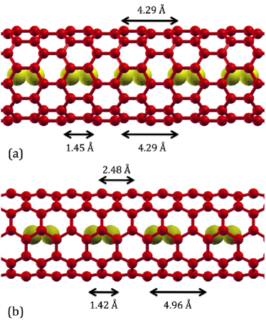
We have simulated Mo wires inside single-walled carbon nanotubes with zigzag and armchair chiralities of different radii. All the armchair nanotubes are metallic, while zigzag nanotubes can behave as a metal or as an insulator, depending on whether is an integer or not. Exhaustive calculations have been performed by testing both dimerized and equidistant encapsulated monoatomic Mo wires with different concentrations (i.e. different separations between Mo dimers in the dimerized chains and between atoms in the equidistant chain) inside the nanotube. We always found the dimerized wires to be the most stable ones for every nanotube. Among zigzag nanotubes, which have a lattice constant of 4.29 Å, the ground state was formed by a dimerized Mo wire unit cell per unit cell of the (9,0) nanotube. This meant that the length of the Mo wire was compressed a 6 % with respect to the free-standing configuration. Among armchair nanotubes, which have a lattice constant of 2.48 Å, the ground state had a dimerized Mo wire unit cell per 2 unit cells of the (5,5) nanotube, which led to a Mo wire stretched an 8 % with respect to the free-standing configuration. We illustrate in Fig. (1) such configurations for the (9,0) zigzag nanotube as well as for the (5,5) armchair one. Encapsulated dimerized Mo wires with concentrations other than these ones, as well as equidistant Mo wires, which were much higher in energy, are revised at the end of this section.
We define the insertion energy of the Mo wire inside the nanotube as the difference between the energy of the whole system (), and the energy of the isolated carbon nanotube () plus times the energy of an isolated Mo atom ( is the number of Mo atoms in the cell). Finally, we divide by in order to normalize.
| (2) |
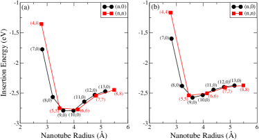
Since we are using localized pseudoatomic orbitals in the basis set, the calculation of the insertion energy must take into account the basis set superposition error (BSSE).bsse This error arises due to the different dimension of the Hilbert spaces associated to the whole system and each of its constituents taken separately. To avoid this error, we have considered the ghost atom method, which consists in including ghost atoms, i.e., pseudo-atomic orbitals without any atomic potential, in the positions of the missing atoms to complete the Hilbert space. The use of ghost atoms has been shown to be very efficient for correcting the BSSE in other systems like, for instance, benzene adsorbed on carbon nanotubes tournus or pentacene physisorbed on gold (001).lee We plot in Fig. (2) the insertion energy as a function of the nanotube radius for different zigzag and armchair nanotubes with and without the BSSE correction. We have found that the BSSE correction has 2 effects in our calculations. On one hand, since the energy of each separated component decreases when its Hilbert space is enlarged, the absolute value of the insertion energy decreases. On the other hand, the BSSE moves the radius for which the minimum insertion energy is obtained to lower values. Therefore, the BSSE correction is essential to produce correct results, and all our calculations have taken it into account.
Fig. (2)(b) and Table I show that the insertion energy mainly depends on the diameter of the nanotube, and is independent of its chirality. The thinnest nanotubes that were found to be able to encapsulate a Mo wire were the (7,0) and the (4,4), both of which have a radius around 2.8 Å. Thinner nanotubes deform a lot upon Mo insertion and lose their symmetry. The minimum in the insertion energy was achieved for (9,0) and (5,5) nanotubes, with radii around 3.5 Å. For thicker nanotubes the bonding between the wire and the nanotube slowly disappears and the insertion energy increases asymptotically towards a constant value, due to the bonding between Mo atoms. This asymptotic limit corresponds to a Mo wire with interatomic distances close to the free-standing case, i.e., without interactions with the nanotube.
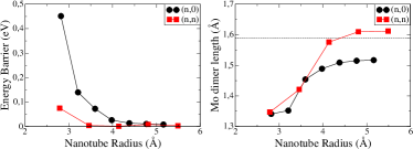
The energy of the wire inside the carbon nanotube also varies as the wire is moved along the axis of the nanotube. We define the diffusion energy barrier as the maximum energy referred to the ground state energy that the wire has to overcome when moving along the nanotube, normalized per Mo atom. This energy barrier has an essential importance in fixing the encapsulated wire, since a too low energy barrier would allow the Mo atoms to move under small forces or thermal agitation, possibly breaking the chain. Further, the Mo atoms are expected to leave the chain just as liquids leave a straw. To obtain this energy barrier we have calculated the energy of the system when the Mo wire is displaced along the carbon nanotube from its relaxed structure, without relaxing again. In Fig. (3)(a), we plot the height of the energy barrier for all of the previous systems. As expected, the value of the energy barrier decreases rapidly when increasing the radius of the nanotube, as the interaction between the nanotube and the wire tends to disappear. We have surprisingly found that chirality in this case plays a role, since armchair nanotubes present a much lower energy barrier. This energy barrier becomes sizeable only for armchair nanotubes with radii shorter than 3 Å, as shown in Fig. 3(a). Interestingly, although the modulus of their insertion energy is about 1 eV lower than that of the system with the optimal radius (see Fig. 2), the formation of the structure with these short radii is still exothermic. Therefore, we expect that encapsulated Mo chains could be seen experimentally in zigzag nanotubes with radii of the order of 3 Å. It is also relevant to note that the energy barrier in zigzag nanotubes is insensitive to their metallic or insulating nature. It is not easy to deduce specific numbers for the atom mobility even assuming an Arrhenius-type law for it, , since we do not know the typical time for activation. For a typical experimental setup, we would use few days seconds. Introducing this number, as well as a slow seconds in the equation above gives temperatures for a working device below . Hence, we predict that the experiments should be performed at moderately low temperatures.
The structure of the chain is also affected by the nanotube. In Fig. (3)(b), we plot the length of the encapsulated Mo dimers as a function of the nanotube radius, with the length of the dimer in the free-standing Mo wire marked by a dashed line. For short nanotube radii, the Mo dimers are compressed by the effect of the nanotube potential. However, they enlarge towards a constant value when the nanotube gets thicker. This constant value for the dimer length is 1 % longer for armchair nanotubes than in the free-standing case, meanwhile inside zigzag nanotubes the dimer length is compressed a 5 %. The Mo dimer length does not converge to the same value as in the free-standing case since we impose a lattice constant condition to commensurate with the lattice constant of the nanotube.
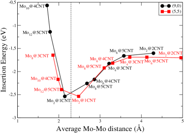
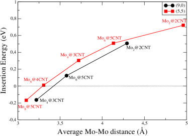
Dimerized Mo wires of different concentrations have also been simulated inside (9,0) and (5,5) carbon nanotubes. We have studied systems with a number of nanotube cells varying from 2 to 5 (where a zigzag cell corresponds to one zigzag unit cell and an armchair cell corresponds to 2 armchair unit cells), and Mo atoms in a dimerized structure. We plot in Fig. (4) the insertion energy of these arrangements, labeled as Mon@CNT, as a function of the average distance between adjacent Mo atoms. The minimum in the insertion energy per Mo atom is found for Mo2@1CNT, for both (9,0) and (5,5) carbon nanotubes. Then, Mo wires tend to resemble as much as possible the free-standing one (dashed line). Increasing the concentration leads to wires with an inter-dimer distance close to the dimer length, which introduces a high repulsion and leads to a rapid increase in the insertion energy. On the other hand, when the Mo concentration is decreased, the insertion energy increases asymptotically to the value of an isolated dimer inside the carbon nanotube.
Encapsulated equidistant Mo wires of the type Mo2@1CNT, which have a high Mo concentration, are not stable inside carbon nanotubes since they tend to dimerize. However, if the Mo concentration is decreased, the energy barriers that the nanotube produces might make the system metastable. We have therefore simulated equidistant Mo wires of different concentrations inside (9,0) and (5,5) carbon nanotubes (Mon@CNT), composed by equidistant Mo atoms inside nanotube cells, in a similar way as we did with the dimerized wires. The results for the insertion energy are shown in Fig. (5). The insertion energy depends mainly on the distance between Mo atoms and is not much affected by the type of nanotube, being a bit lower in the case of zigzag nanotubes. In case of encapsulated equidistant Mo wires with an interatomic distance between Mo atoms shorter than around 3 Å we found that the Mo atoms tend to dimerize and the wire is not able to retain its equidistant arrangement. We also found that the insertion energy increases as the distance between Mo atoms is increased, and becomes positive for Mo-Mo distances larger than 3.25 Å. Therefore, equidistant Mo wires encapsulated inside carbon nanotubes could be achieved with an interatomic distance between 3.00 Åand 3.25 Å, which corresponds to the range where the insertion energy is negative. However, these values are more than 2 eV higher than in the dimerized arrangement.
Unlike the dimerized Mo wires, the equidistant wires are magnetic, with an antiferromagnetic (AFM) coupling between adjacent Mo atoms and a magnetic moment of around 5 B per Mo atom. A ferromagnetic (FM) state can also be found, with an energy difference per Mo atom between the FM and the AFM which is larger than 300 meV for the structures with negative insertion energy and that asymptotically decreases towards zero as the distance between Mo atoms increases.
IV Electronic Structure and Transport Properties
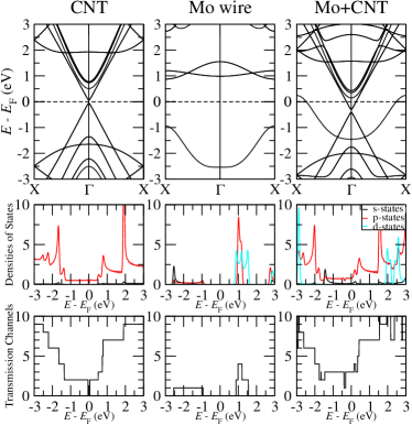
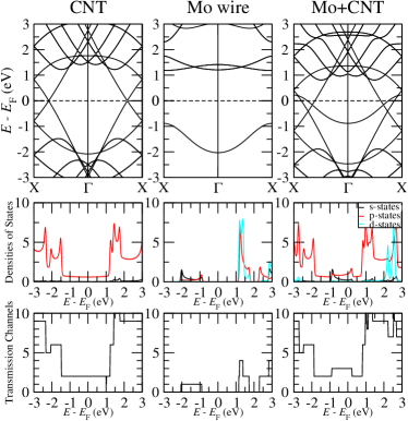
We have calculated the band structure, densities of states and transmission channels of the Mo2@1CNT for different thicknesses and chiralities. Figs. (6) and (7) show the results for the cases corresponding to the (9,0) and (5,5) nanotubes, respectively. To clarify the discussion, we have also calculated the above properties for the empty nanotube and the isolated Mo wire with their geometries fixed to those within the Mo2@1CNT systems. The ground state of the free-standing Mo wire exhibits a band below the Fermi level ( is the direction of the wire) that leads to a transmission channel between -2 and -1 eV.amador This band is preserved when the wire is compressed (Fig. (6)) or stretched (Fig. (7)) inside the carbon nanotubes. However, it moves up in energy as a consequence of the encapsulation, eventually reaching the Fermi level. This leads to a low-bias total conductance of 3 due to 3 transmission channels at the Fermi level, one from the band of the Mo wire and two others from the bands of the carbon nanotube.
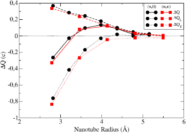

In order to analyze in more detail the bonding between the Mo wire and the CNT, which is related to the displacement of some bands and has important implications in the transport properties, we have calculated the change in the electronic charge of the Mo atoms encapsulated in the different nanotubes investigated. We take as reference the charge in the ground state of the infinite free-standing Mo wire. The results are shown in Fig. (8). We note that, inside very thin nanotubes, Mo tends to lose charge, meanwhile the charge transfer changes its sign when the nanotube radius increases, leading to a maximum for (10,0) and (6,6) nanotubes. For nanotubes with large enough radii, the charge transfer tends to 0 as the interaction between the wire and the nanotube disappears. Therefore, Mo wires inside (9,0) and (5,5) nanotubes, which correspond to the most stable configurations, increase their charge. We have also calculated the charge variation in each cartesian orbital. We have found that the , and orbitals are only slightly affected by the encapsulation; , , and (which are transversal orbitals) increase their charge, and and (which are longitudinal orbitals) lose charge, which is consistent with the band crossing the Fermi level (see Figs. (6) and (7)). Fig. (8) also shows the charge variation in the transversal and longitudinal orbitals separately. The charge transfer towards Mo transversal orbitals is favored by the encapsulation, decreases linearly as the nanotube radius increases and is still present for relatively large nanotube radii. On the other hand, Mo longitudinal orbitals lose charge for small nanotube sizes, but this loss rapidly disappears (exponentially) when the nanotube radius increases. The excess of charge in the transversal orbitals and its disappearance for large CNT radii can be explained as an effect of the bonding between these orbitals and the orbitals from the C atoms, which is reflected in the strong hybridization between them.
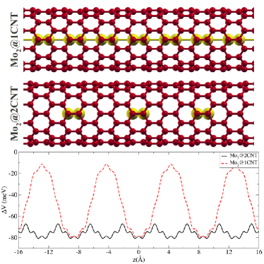
We have also analyzed the change in the electrostatic potential at the nanotube walls when the Mo wire is introduced Victor3 . Such potential could be able to trap electrons,Lee02 ; Cho03 produce entangled electrons pairs and tailor the interaction between static and flying qubits Gun06 . To estimate this change, which is related to charge transfer, structural modification and hybridization between the Mo atoms and the nanotube, we have calculated the electrostatic potential at the walls of the nanotubes with and without the Mo wire and subtracted one from the other, i.e. . We note that this potential only depends on the coordinate due to the axial symmetry. We plot in Fig. (9) for 2 dimerized Mo wires with different concentrations inside a (10,0) carbon nanotube. As expected, clearly defined wells appear around the dimers, with a valley in the position of each Mo atom due to the presence of more negative charge at these points. The absolute maximum in appears at the middle point between dimers. For Mo2@2CNT, has enough room to reach nearly zero, meanwhile for Mo2@1CNT this is not possible.
The displacement of the band from the Mo wire towards the Fermi level is concomitant with the charge variation of these states, as illustrated in Fig. (8) and discussed above. Therefore, regardless of the chirality of the system, if the nanotube radius is small enough to produce a noticeable charge variation in the longitudinal orbitals, the band of the Mo wire will enter the Fermi level and contribute to the conduction (see Figs. (6) and (7)). By calculating the band structure and transmission channels of each structure, we have found that the band enters the Fermi level for zigzag nanotubes up to the (10,0) and for armchair nanotubes up to the (6,6), which means that there is a transition radius around 4.2 Å. This implies that, if the nanotube has an appropriate radius, when the insulator dimerized Mo wire is encapsulated, the resulting system has metallic behavior, even if the nanotube is also an insulator. As an example, we plot in Fig. (10) the density of states in real space integrated around the Fermi level for the dimerized Mo wire inside the zigzag (10,0) nanotube, and we compare it with the corresponding density of states of its isolated constituents. Since both the isolated nanotube and Mo wire are insulators, there is no density of states around the atoms as illustrated in the picture. However, when the hybrid quasi one-dimensional system is formed, a noticeable amount of density of states is present. This density of states is delocalized through the whole system (both C atoms and Mo atoms) and results from the hybridization between the band of Mo with the bands of C around the Fermi level. These states make the hybrid system conductive at low bias voltage. Therefore, encapsulating Mo wires in CNT is a way to create conductive quasi one-dimensional hybrid nanostructures from their insulating constituents.
V Conclusions
We have investigated monoatomic chains of molybdenum encapsulated in single walled carbon nanotubes of different chiralities. The electronic structure and the optimal atomic arrangement have been calculated using the DFT code SIESTA with the generalized gradient approximation. We have also used the non-equilibrium Green’s functions formalism as implemented in the SMEAGOL code smeagol to calculate the conductance in the ohmic regime.
We have found that the insertion energy mainly depends on the diameter of the nanotube, and is independent of its chirality. The thinnest nanotubes able to encapsulate a Mo wire were the (7,0) and the (4,4), both of them with a radius around 2.8 Å. Among zigzag nanotubes, which have a lattice constant of 4.29 Å, the ground state was formed by a dimerized Mo wire unit cell per unit cell of the (9,0) nanotube. This meant that the length of the Mo wire was compressed a 6 % with respect to the free-standing configuration. Among armchair nanotubes, which have a lattice constant of 2.48 Å, the ground state had a dimerized Mo wire unit cell per 2 unit cells of the (5,5) nanotube, which led to a Mo wire stretched an 8 %. These nanotubes, which are the optimal for encapsulating Mo wires, have radii around 3.5 Å.
We have also calculated the diffusion energy barrier, which decreases rapidly when the radius of the nanotube is increased. We have demonstrated that chirality in this case plays a role, since armchair nanotubes present a lower energy barrier. A too low diffusion energy barrier could hamper however the experimental production of such structures since the wire would be able to move easily along the nanotube under mechanical or thermal perturbations.
Finally, we have shown that the bonding between the transversal orbitals of Mo and the orbitals of the C atoms upon encapsulation leads to electronic charge transfer towards those Mo transversal orbitals. We have found that this transfer is still present for relatively large nanotube radii. The band of the insulator free-standing dimerized Mo wire was preserved when the wire was compressed or stretched inside the carbon nanotubes but it moved up in energy as a consequence of the encapsulation, eventually reaching the Fermi level and contributing with the bands of the CNT to a low-bias total conductance of 3 . The band crossed the Fermi level for zigzag nanotubes up to the (10,0) and for armchair nanotubes up to the (6,6). This implies that, if the nanotube has an appropriate radius, like the (9,0) or the (5,5), when the insulator dimerized Mo wire is encapsulated the resulting system has always metallic behavior, even if the nanotube is also an insulator. Therefore, encapsulating Mo wires in CNTs can lead to metallic nanostructures comprised of parts which are insulating on their own.
Acknowledgements.
This work was supported by the Marie Curie network NanoCTM, by the Spanish Ministry of Education and Science in conjunction with the European Regional Development Fund (Projects FIS2008-02490/FIS and FIS2009-07081), and by Junta de Castilla y León (Project GR120). VMGS thanks the Spanish Ministerio de Ciencia e Innovación for a Juan de la Cierva fellowship.References
- (1) A. Vega, C. Demangeat, and J. C. Parlebas, Handbook of Magnetic Materials. K.H.J. Buschow. Elsevier North-Holland, 199-288 (2003).
- (2) M. C. Desjonquères and D. Spanjaard, Concepts in Surface Physics. Springer (1993).
- (3) Y. Shiratsuchi, M. Yamamoto, and S. D. Bader, Progress in Surface Science 82, 121 (2007).
- (4) G. A. Somorjai and J. Y. Park, Surface Science 603, 1293 (2009).
- (5) R.H. Baughman, A.A. Zakhidov, and W. de Heer, Science 297, 787 (2002).
- (6) M. Monthioux, Carbon 40, 1809 (2002).
- (7) C. Guerret-Piécourt, Y.Le Bouar, A. Lolseau, and H. Pascard, Nature 372, 761 (1994).
- (8) S. Seraphin, D. Zhou, and J. Jiao, J. Appl. Phys. 80, 2097 (1996).
- (9) A. Chu et al., Chem. Mater. 8, 2751 (1996).
- (10) A.A. Setlur, J.M. Lauerhaas, J.Y. Dai, and R.P.H. Chang, Appl. Phys. Lett. 69, 345 (1996).
- (11) L.C. Qin, J. Mater. Sci. Lett. 16, 457 (1997).
- (12) N. Grobert, W.K. Hsu, Y.Q. Zhu, J.P. Hare, H.W. Kroto, D.R. Walton, M. Terrones, H. Terrones, P. Redlich, M. Rühle, R. Escudero, and F. Morales, Appl. Phys. Lett. 75, 3363 (1999).
- (13) Y. Qin, S.M. Lee, A. Pan, U. Gösele, and M. Knez, Nano Lett. 8, 114 (2008).
- (14) Y. Qin, L. Liu, R. Yang, U. Gösele, and M. Knez, Nano Lett. 8, 3221 (2008).
- (15) H. Muramatsu, T. Hayashi, Y.A. Kim, D. Shimamoto, M. Endo, M. Terrones, and M.S. Dresselhaus, Nano Lett. 8, 237 (2008).
- (16) V. Meunier, H. Muramatsu, T. Hayashi, Y.A. Kim, D. Shimamoto, H. Terrones, M.S. Dresselhaus, M. Terrones, M. Endo and B.G. Sumpter, Nano Lett. 9, 1487 (2009).
- (17) Y. Tao, H. Muramatsu, T. Hayashi, Y.A. Kim, D. Shimamoto, M. Endo, K. Kaneko, M. Terrones, and M.S. Dresselhaus, Appl. Phys. Lett. 94, 113105 (2009).
- (18) A. Loiseau and H. Pascard, Chem. Phys. Lett. 256, 246 (1996).
- (19) L.H. Guan, K. Suenaga, Z.J. Shi, Z.N. Gu, and S. Iijima, Nano Lett. 7, 1532 (2007).
- (20) L.H. Guan, K. Suenaga, S. Okubo, T. Okazaki, and S. Iijima, J. Am. Chem. Soc. 130, 2162 (2008).
- (21) C.K. Yang, J. Zhao, and J.P. Lu, Phys. Rev. Lett. 90, 257203 (2003).
- (22) V.V. Ivanovskaya, C. Köhler, and G. Seifert, Phys. Rev. B 75, 075410 (2007).
- (23) W. Kohn and L. J. Sham, Phys. Rev. 140, A1133 (1965).
- (24) A. García-Fuente, A. Vega, V. M. García-Suárez, and J. Ferrer, Nanotechnology, in press 2010.
- (25) J. M. Soler, E. Artacho, J. D. Gale, A. García, J. Junquera, P. Ordejón, and D. Sánchez-Portal, J. Phys.: Condens. Matter 14, 2745 (2002).
- (26) A. R. Rocha, V. M. García-Suárez, S. W. Bailey, C. J. Lambert, J. Ferrer and S. Sanvito, Phys. Rev. B73, 085414 (2006).
- (27) J. P. Perdew, K. Burke, and M. Ernzerhof, Phys. Rev. Lett. 77, 3865 (1996).
- (28) V. M. García-Suárez, C. M. Newman, C. J. Lambert, J. M. Pruneda, and J. Ferrer, J. Phys.: Condens. Matter 16, 5453 (2004).
- (29) N. Troullier and J. L. Martins, Phys. Rev. B 43, 1993 (1991).
- (30) L. Kleinman and D. M. Bylander, Phys. Rev. Lett. 48, 1425 (1982).
- (31) W. Zhang, X. Ran, H. Zhao, and L. Wang, J. Chem. Phys. 121, 7717 (2004).
- (32) V. M. García-Suárez, J. Ferrer, and C. J. Lambert, Phys. Rev. Lett. 96, 106804 (2006).
- (33) V. M. García-Suárez, J. Ferrer, and C. J. Lambert, Phys. Rev. B 74, 205421 (2006).
- (34) W. H. Press, S. A. Teukolsky, W. T. Vetterling, and B. P. Flannery,Numerical Recipes in Fortran, 2nd ed. (Cambridge University Press, Cambridge, 1992).
- (35) S. Datta, Electronic Transport in Mesoscopic Systems. Cambridge University Press, Cambridge, UK, 1995.
- (36) S. F. Boys and F. Bernardi, Mol. Phys. 19, 553 (1970).
- (37) F. Tournus, and J-C. Charlier, Phys. Rev. B 71, 165421 (2005).
- (38) K. Lee, J. Yu, and Y. Morikawa, Phys. Rev. B 75, 045402 (2007).
- (39) J. Lee, H. Kim, S.-J. Kahng, G. Kim, Y.-W. Son, J. Ihm, H. Kato, Z. W. Wang, T. Okazaki, H. Shinohara, and Y. Kuk, Nature (London) 415, 1005 (2002).
- (40) Y. Cho, S. Han, G. Kim, H. Lee, and J. Ihm, Phys. Rev. Lett. 90, 106402 (2003).
- (41) D. Gunlycke, J. H. Jefferson, T. Rejec, A. Rams̆ak, D. G. Pettifor, and G. A. D. Briggs, J. Phys.: Condens. Matter 18, S851 (2006).