Atomistic study of electronic structure of PbSe nanowires
Abstract
Lead Selenide (PbSe) is an attractive ‘IV-VI’ semiconductor material to design optical sensors, lasers and thermoelectric devices. Improved fabrication of PbSe nanowires (NWs) enables the utilization of low dimensional quantum effects. The effect of cross-section size (W) and channel orientation on the bandstructure of PbSe NWs is studied using an 18 band tight-binding theory. The bandgap increases almost with the inverse of the W for all the orientations indicating a weak symmetry dependence. [111] and [110] NWs show higher ballistic conductance for the conduction and valence band compared to [100] NWs due to the significant splitting of the projected L-valleys in [100] NWs.
Appealing PbSe bulk properties: Lead selenide (PbSe) is a narrow, direct band gap semi-conductor material ( = 0.16eV at 4K PbSe_data ; Lent_TB ) with useful electrical, optical and lattice properties PbSe_optic ; PbSe_bulk_thermo ; MEgen_1 . It is used extensively in optical devices Kang_and_wise ; PbSe_optic , lasers PbSe_laser ; PbSe_laser_2 and thermoelectric devices PbSe_NW_fab_3 ; PbSe_bulk_thermo ; PbSe_NW_thermo . The large Bohr exciton radius of about 46nm in PbSe makes it a suitable system to study quantum confinement effects on electrons and holes Kang_and_wise ; PbSe_NW_fab_1 ; PbSe_NW_fab4 ; PbSe_qdot . Recent progress in multiple exciton generation (MEG) in PbSe with higher optical efficiency has renewed interest in the optical properties of PbSe MEgen_1 . Extremely low thermal conductivity of PbSe ( 2 W/m-K in bulk PbSe_low_kappa to 0.8 W/m-K in NWs PbSe_NW_low_kappa ) also makes it a suitable thermoelectric material PbSe_bulk_thermo ; PbSe_NW_thermo . PbSe can become a preferable material over Lead Telluride (PbTe) due to the higher availability of selenium (Se) compared to tellurium (Te) PbSe_singh_DFT .
Nanostructures PbSe : One dimensional nanostructures of PbSe like nanowires (NW) and nanorods (NR) combine the interesting bulk material properties as well as the quantum confinement effects which can lead to better thermoelectric PbSe_NW_thermo ; PbSe_low_kappa ; PbSe_NW_low_kappa and optical PbSe_optic devices. The analysis of the physical properties in PbSe NWs will require proper understanding of the electronic structure, which is the theme of the present paper.
PbSe NW growth technologies: With recent advances in the growth and process technology, the fabrication of PbSe NWs have become very efficient and controlled. PbSe NWs are developed using a variety of methods like, chemical vapor transport (CVT) method PbSe_NW_fab_3 , oriented nano-particle attachment PbSe_NW_fab_1 , electro-deposition without catalyst PbSe_NW_fab4 and with catalyst PbSe_NW_fab_5 , hyper-branching PbSe_NW_fab_2 , growing PbSe structures on phosphate glass PbSe_qdot_fab , etc. These methods enable PbSe NWs fabrication with a variety of growth directions and surfaces.
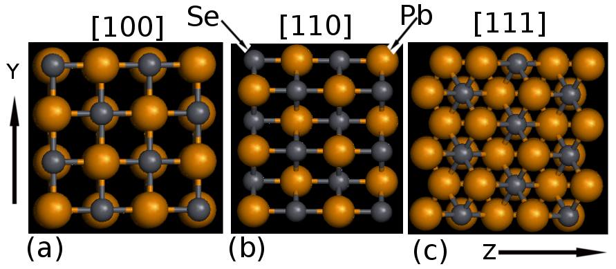
PbSe crystal structure: Bulk PbSe has a stable rocksalt structure with a co-ordination number of six at room temperature (300K) and normal atmospheric pressure PbSe_singh_DFT ; PbSe_data . The lattice constant is 0.6121 nm PbSe_data at T = 4K, which is also utilized in our bandstructure calculations. The PbSe NWs are constructed using the same bulk structure with three different wire axis orientations of [100], [110] and [111] (Fig. 1).
Electronic Structure calculation: The main methods for analyzing the lead salt structures are (1) continuum method like 4/8-band kp Kang_and_wise , (2) semi-empirical atomistic methods like tight-binding (TB)delure_TB ; Lent_TB , pseudo-potential approaches PbSe_EPM_2 or (3) first principles methods PbSe_qdot ; PbSe_DFT ; PbSe_DFT_1 ; PbSe_singh_DFT . The 4/8-band kp method captures some quantum confinement effects, however, it fails to capture the interaction of various valleys present along the L-K and L-X directions, the band anisotropy and the correct frequency dependent dielectric function PbSe_qdot ; PbSe_EPM_2 ; delure_TB . The first principle calculations are highly accurate but the demand for computational power is very high and these methods are limited to solving only small structures with few thousand atoms Klimeck_TB ; delure_TB . The semi-empirical methods are versatile in terms of the involved physics and can handle a large number of atoms ( 10 million atoms Klimeck_TB ) making them suitable for electronic structure and transport calculation in realistic device structures. However, an integral part of these methods is the requirement of correct semi-empirical parameter sets to properly represent the electronic structure properties like bandgaps, effective masses, wave-function symmetry, etc. In this work we utilize a semi-empirical atomistic TB method based on formulation with spin orbit coupling (SOC) optimized for bulk Pb salts by Lent et al Lent_TB to calculate the electronic structure in NWs. The inclusion of SOC is important in PbSe since both CB and VB have strong p-contributions from Pb and Se atoms, respectively PbSe_qdot ; delure_TB .
Surface atoms: The TB parameters developed for bulk Pb salts Lent_TB are also applied to nanostructures with finite boundaries. The surface atoms are not passivated for Pb salt nanostructures. It has been previously shown that surfaces do not introduce states in the energy gaps of the bulk band structure, even though they are not passivated delure_TB and the same is obtained in the present study. The surface states are mainly p-like for Pb salts which are strongly coupled with orbitals of atoms at the interior unlike the zinc-blende semiconductors where atoms are described by hybrid orbitals which remain uncoupled at surfaces, forming dangling bonds Lee_sp3 . The lack of surface passivation has also been pointed out by the first principle calculations in stoichiometric Pb salt nanostrutures PbSe_DFT_1 ; PbSe_qdot .
Electronic Structure: The bulk effective masses calculated using the TB parametrization in Ref. Lent_TB is obtained for (i) electrons as = = 2.4 (1.85) and (ii) holes as = = 2.9 (2.0). The values in the parenthesis are from Ref.PbSe_data . The TB parametrization in Ref. Lent_TB () is preferred over the parametrization in Ref. delure_TB () since the model captures the mass anisotropy quite well, an important requirement for TB models as pointed in Ref. PbSe_EPM_2 .
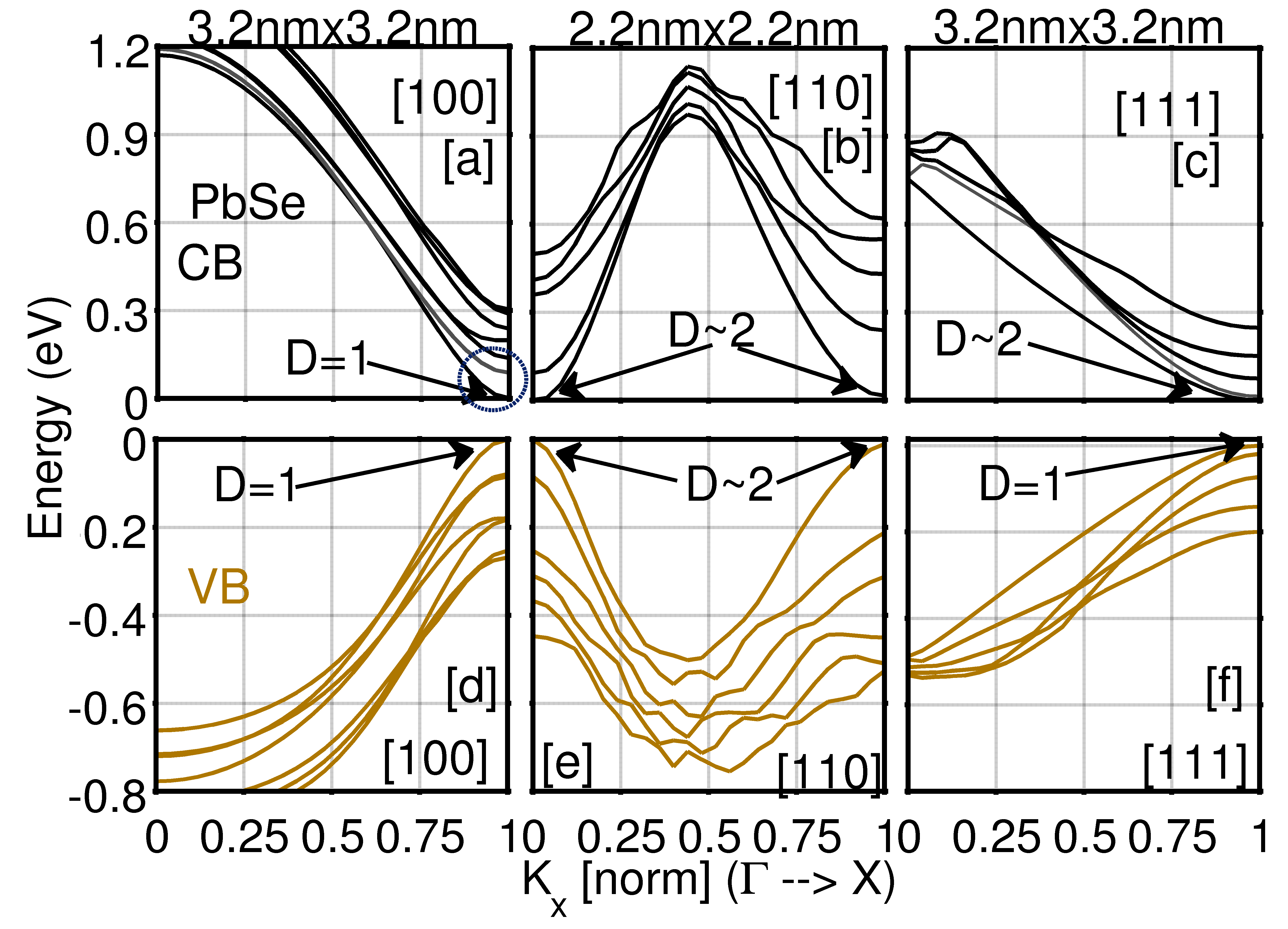
The bandstructure of conduction (CB) and valence band (VB) for PbSe nanowires are shown in Fig. 2 for 3 different wire orientations. For all the wires the conduction band minima (CBM) and valence band maxima (VBM) are normalized to zero to enable a better comparison of the valleys. Few important points to observe are, (i) bulk L valleys are projected at the Brillioun zone (BZ) edge at X for all orientations (Fig. 2). The [110] wire has an additional projected valley at the position (Fig.2 b, e), (ii) [100] NW show a degeneracy (D) of 1 for both CB and VB due to strong valley splitting, however [110] and [111] NWs show a D of nearly 2 (extremely small valley splitting) for the positive ‘k’ states.

Bandgap and bandedge variation: The CBM and VBM variation with cross-section size (W) and orientation are shown in Fig. 3 a. All the orientations show quite similar band-edge variation with W. As the cross-section size decreases the geometrical confinement increases which pushes the CBM (VBM) higher (lower) in energy. The variation in the bandedges with W also compare surprisingly well with a previous 4-band kp calculation done for [111] cylindrical PbSe NWs PbSe_NW_kp . The bandgap variation with W in PbSe NWs can be fitted to the following analytical expression,
| (1) |
where represents the power law dependence on W.
For [111] NWs the value of is 1.726 (0.8734). For [110] NWs these values are () 1.564 (0.8592) and for [100] NWs these values are () 1.87(1.072). The bandgap values (Fig. 3 b) roughly show an inverse relation with W for all the NW orientations which is very different from the prediction of effective mass approximation (Eg ). Similar results for Eg have been obtained by other independent calculations carried out in PbSe nanostructures using first principle calculations PbSe_qdot as well as TB calculations delure_TB . This justifies the application of TB electronic structure calculation which correctly captures the quantum confinement effects in ultra-scaled PbSe NWs.
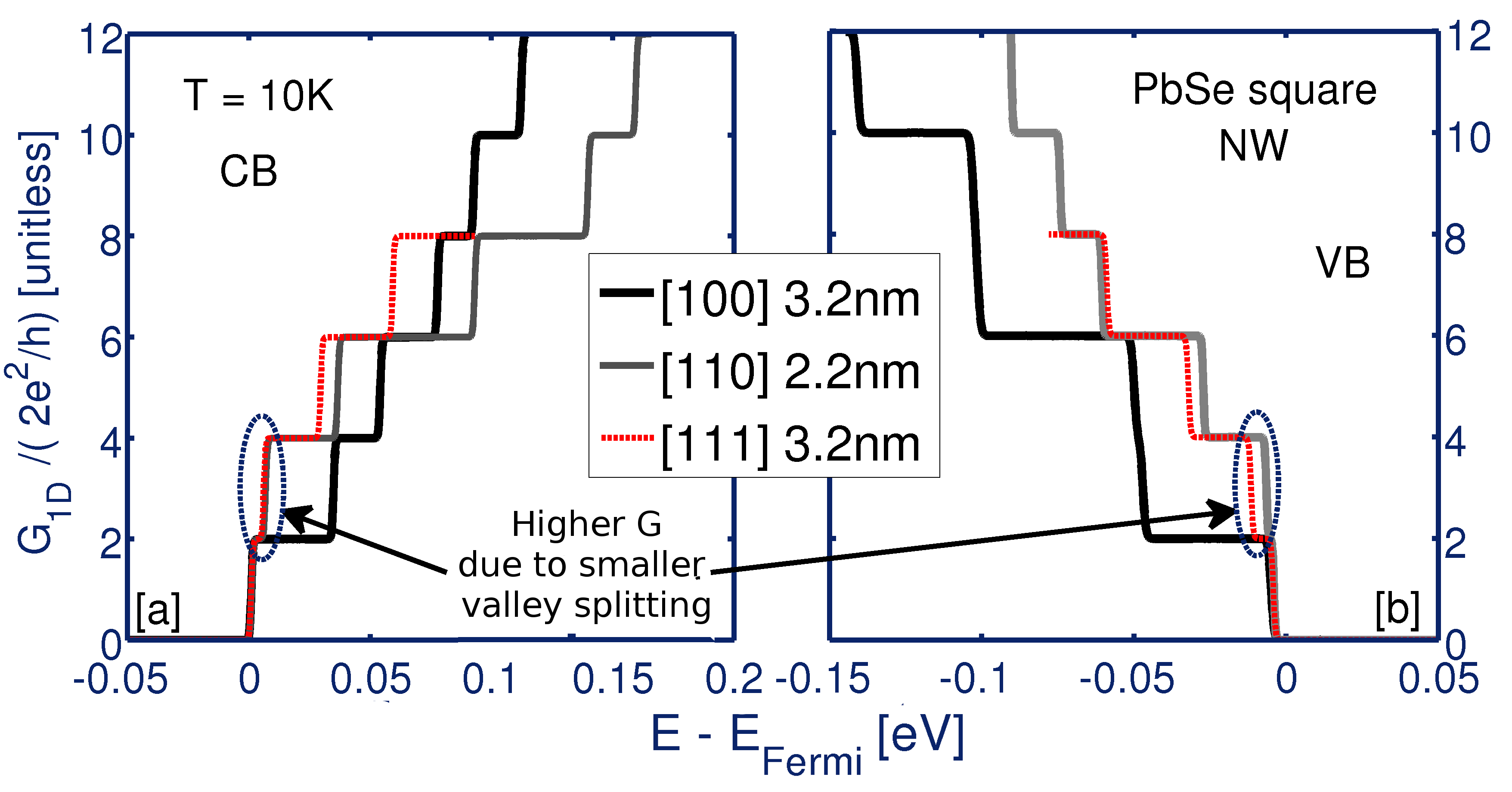
Ballistic conductance: Transport properties of PbSe NWs are revealed by the electronic conductance which is calculated using Landauer’s formula Land . Figure 4 shows the normalized 1D ballistic conductance for electrons in the PbSe NWs for 3 different orientations. [110] and [111] oriented wires show higher G value for both the CB and the VB compared to [100] NWs. A larger valley splitting in the CB and the VB in [100] NWs decrease the conductance compared to the other two orientations. The normalized conductance increases in steps of 2 for [100] NWs for the CB but not for the VB (Fig. 4) which shows that the CB and the VB are not entirely symmetric in energy, a result similar to the one given in Ref. PbSe_EPM_2 . Thus, transport characteristics show the influence of geometrical confinement and channel orientation.
Summary and Outlook: PbSe NWs have tremendous potential of becoming the next generation thermoelectric and optical devices. The proper understanding of the physical properties of these ultra-scaled PbSe nanowires will depend strongly on the correct electronic structure calculation. We have presented the application of semi-empirical tight-binding theory to these NWs to understand the variation of conduction and valence bands and the position of the important energy valleys. The variation of the bandgap and the bandedges with NW cross-section size is strongly influenced by the cross-section size and channel orientation. Simple effective mass theory cannot predict the bandgap variation. The amount of valley splitting is strongly dependent on the type of geometrical confinement as reflected in the ballistic conductance of the PbSe NWs. [110] NWs provide the maximum ballistic conductance for both the CB and VB. The tight-binding analysis of electronic structure opens door to explore the optical and thermoelectric effects in PbSe NWs.
Financial support from MSD Focus Center, under SRC, Nanoelectronics Research Initiative through MIND, NSF (Grant No. OCI-0749140) and Purdue University is acknowledged. Computational support from nanoHUB.org, an NCN operated and NSF (Grant No. EEC-0228390) funded project is also gratefully acknowledged.
References
- (1) O. Madelung, U. Rössler, and M. Schulz, Springer Materials - The Landolt-Börnstein Database(2010)
- (2) C. S. Lent, M. A. Bowen, J. D. Dow, R. S. Allgaier, O. F. Sankey, and E. S. Ho, Superlattices and Microstructures 2, 491 (1986)
- (3) J. Diezhandino, G. Vergara, G. Pérez, I. Génova, M. T. Rodrigo, F. J. Sánchez, M. C. Torquemada, V. Villamayor, J. Plaza, I. Catalán, R. Almazán, M. Verdú, P. Rodríguez, L. J. Gómez, and M. T. Montojo, Applied Physics Letters 83, 2751 (2003)
- (4) I. Kudman, Jour. of Mat. Science 7, 1027 (1972)
- (5) M. Ji, S. Park, S. T. Connor, T. Mokari, Y. Cui, and K. J. Gaffney, Nano Letters 9, 1217 (2009)
- (6) I. Kang and F. W. Wise, J. Opt. Soc. Am. B 14, 1632 (1997)
- (7) J. Fürst, H. Pascher, T. Schwarzl, M. Böberl, G. Springholz, G. Bauer, and W. Heiss, Applied Physics Letters 84, 3268 (2004)
- (8) M. Rahim, A. Khiar, F. Felder, M. Fill, and H. Zogg, Applied Physics Letters 94, 201112 (2009)
- (9) M. Fardy, A. I. Hochbaum, J. Goldberger, M. M. Zhang, and P. Yang, Advanced Materials 19, 3047 (2007)
- (10) W. Liang, A. Hochboum, M. Fardy, M. Zhang, and P. Yang, Nano Research 2, 394 (2009)
- (11) K. S. Cho, D. V. Talapin, W. Gaschler, and C. B. Murray, Journal of Americal Chemical Society 127, 7140 (2005)
- (12) J. E. Hujdic, D. K. Taggart, S.-C. Kung, and E. J. Menke, The Journal of Physical Chemistry Letters 1, 1055 (2010)
- (13) Y. Gai, H. Peng, and J. Li, Jour. Phys. Chem. C 113, 21506 (2009)
- (14) W. Liang, O. Rabin, A. I. Hochbaum, M. Fardy, M. Zhang, and P. Yang, Nano Research 2, 394 (2009)
- (15) D. Gray, AIP and McGraw-Hill(1972)
- (16) L. Zhang and D. J. Singh, Phys. Rev. B 80, 075117 (2009)
- (17) X. S. Peng, G. W. Meng, J. Zhang, X. F. Wang, C. Z. Wang, X. Liu, and L. D. Zhang, Journal of Material Research 17 (2002)
- (18) M. J. Bierman, Y. K. A. Lau, and S. Jin, ACS Nanoletters 7, 2907 (2007)
- (19) A. Lipvoskii, E. Kolobkova, V. Petrikov, I. Kang, A. Olkhovets, T. Krauss, M. Thomas, J. Silcox, F. Wise, Q. Shen, and S. Kycia, Applied Physics Letters 71, 3406 (1997)
- (20) G. Allan and C. Delerue, Phys. Rev. B 70, 245321 (2004)
- (21) J. M. An, A. Franceschetti, S. V. Dudiy, and A. Zunger, Nano Letters 6, 2728 (2006)
- (22) M. Lach-hab, D. A. Papaconstantopoulos, and M. J. Mehl, Journal of Physics and Chemistry of Solids 63, 833 (2002)
- (23) A. Franceschetti, Phys. Rev. B 78, 075418 (2008)
- (24) G. Klimeck, S. S. Ahmed, N. Kharche, M. Korkusinski, M. Usman, M. Prada, and T. Boykin, Transaction on Electron Devices, IEEE 54, 2090 (2007)
- (25) S. Lee, F. Oyafuso, P. von Allmen, and G. Klimeck, Phys. Rev. B 69, 045316 (2004)
- (26) S. V. Goupalov, On arxiv.org, arXiv:1012.2424v1, url:http://arxiv.org/abs/1012.2424(2010)
- (27) R. Landauer, IBM J. Res. Dev. 1, 223 (1957)