Spin Polarized and Valley Helical Edge Modes in Graphene Nanoribbons
Abstract
Inspired by recent progress in fabricating precisely zigzag-edged graphene nanoribbons and the observation of edge magnetism, we find that spin polarized edge modes with well-defined valley index can exist in a bulk energy gap opened by a staggered sublattice potential such as that provided by a hexagonal Boron-Nitride substrate. Our result is obtained by both tight-binding model and first principles calculations. These edge modes are helical with respect to the valley degree of freedom, and are robust against scattering, as long as the disorder potential is smooth over atomic scale, resulting from the protection of the large momentum separation of the valleys.
pacs:
73.20.-r 81.05.UwIntroduction.— The appearance of edge states is one of the most peculiar phenomena in solid state systems. They are often connected to topologically non-trivial bulk properties, e.g. non-zero Chern numbers in quantum Hall systems TKNN ; Hatsugai , or odd numbers in time-reversal invariant topological insulators Kane2 . The edge states in quantum Hall systems are robust against all kinds of disorders and interactions Niu1 , while those in the latter systems can survive scatterings that preserve the time reversal symmetry Kane2 ; Kane1 . The edge states in graphene with zigzag terminations belong to a different category. Such states connect the two different valleys and projected along the edge direction and their presence is dictated by the bulk topological charge WangYao . It is of great interest to utilize these unusual states for various applications Louie ; Kyle .
Recently, zigzag-edged graphene nanoribbons have been fabricated with precision by unzipping carbon nanotubes ZigzagCut ; AnisotropicEtching ; ZigzagReconstruct . Without electron-electron interaction, the edge states form a completely flat edge band connecting the two valleys with large momentum separation ExpGraphene ; RMPGraphene . When interaction is taken into account, due to the singular density of states, spins on the edge become spontaneously polarized resulting in an edge ferromagnetism Louie ; ZigMagAbinitio , which has been confirmed by a recent experiment ZigMagExp . The spin polarized edge states are dispersive in momentum space, making them useful for current transport. Unfortunately, without a bulk gap, the effect of edge states would be overwhelmed by the contribution from the bulk states.
In this Letter, we show that for zigzag-edged graphene nanoribbons spin polarized dispersive edge states can exist and remain robust in a bulk gap opened by a staggered sublattice potential. Such potential can be realized, for example, by a hexagonal Boron-Nitride substrate. The edge modes are then tied to the conduction or valance band edges, and with spontaneous spin polarization due to interaction effects, one spin branch of the edge modes is pushed into the bulk gap forming a conducting channel in the bulk insulating state. We show that such spin-polarized states within the bulk gap remain robust under scattering with correlation length longer than the lattice constant. We also perform first principles calculations to further support our predictions.
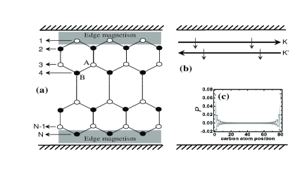
Tight-Binding Model.— Figure 1.(a) illustrates the schematic setup of a zigzag-edged graphene nanoribbon in the presence of a staggered sublattice potential. A tight-binding Hamiltonian that incorporates phenomenologically the edge spin-polarization can be written as:
| (1) |
where () is the electron creation (annihilation) operator on site , and is the component of Pauli matrices. The first term is the nearest neighbor hopping with being the hopping energy. The second term represents the effect of edge ferromagnetism which stems from electron-electron interaction, and is a phenomenological parameter put in by hand at present stage, and its value will be determined later from the first-principles method. The last term corresponds to the staggered sublattice potentials: = for sublattice A (), and for sublattice B (). In our analysis of tight-binding model, we measure the energy , magnetization , potential , and disorder strength in units of the hopping energy .
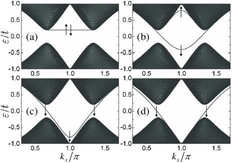
The energy spectrum of graphene nanoribbons with zigzag termination can be numerically obtained by diagonalizing the Hamiltonian in momentum space for each crystal momentum along the edge direction which we take as -axis. Figure 2 shows the evolution of the energy spectrum as functions of staggered sublattice potential and edge magnetization for fixed ribbon width (about 852 Å). For clarity, only the edge states from the upper boundary are shown. Panel (a) shows the doubly-degenerate flat-bands connecting the two Dirac points and . We observe that a bulk energy gap is opened by inversion symmetry breaking due to the staggered sublattice potentials.
Figures 2.(b)-(d) plot the band structures when is taken to be , , and , respectively. We find that, due to the different degrees of localization of the states in edge band WangYao , the magnitude of the energy splitting of the edge bands is -dependent: the spin-up edge band bends upward, while the spin-down edge band bends downward. This makes edge band dispersive hence capable of conducting charge current. Moreover, for a fixed sublattice potential , we find that along with the increasing of the edge magnetization from 0.6 [see panel (b)] to 1.0 [see panel (c)], the spin-down edge band gradually approaches the bulk valence band, and eventually touches and emerges into the bulk valence band (at ). This creates gapless edge modes tied to each valley, which is similar to the finding in Ref. WangYao except that the edge modes here are spin-polarized.
From the energy spectra, we observe that the two edge states in the bulk energy gap propagate along opposite directions. Due to the same flat-band origin, they are localized at the same upper boundary. We also note that the edge states in the gap have well-defined valley index or . The situation is schematically shown in Fig. 1(b): the edge states with same spin but different valley indices propagate oppositely along the same boundary. This can be natually termed as a spin-polarized quantum-valley Hall state.
Robustness of Spin-Polarized Edge Mode.— From the above analysis, we notice that for the fixed bulk gap, the spin polarized edge state is gapped for weak edge magnetization, while the edge state becomes gapless when the edge magnetization approaches a critical . These edge states in the gap provide conducting channels for spin-polarized transport. However, to be useful for practical applications, they need to be robust against impurity scattering. In the following, we shall investigate the robustness of the edge state in the presence of impurities, and show that both gapped and gapless edge states are robust against scattering due to the large momentum separation between the valleys and .
It is known that the impurity scattering in graphene mainly comes from the long-range Coulomb scatterers LongRangeDisorder . We assume that the impurity potential at each site takes a Gaussian form DisorderForm :
| (2) |
where the summation is over all sites, is the local disorder strength at site , and is the correlation length. We define an effective disorder strength from and definition :
| (3) |
The numerical simulations are performed within the same setup of Ref. QuantumSpinHallEffect including only the left and right semi-infinite leads. The two-terminal conductance can be calculated from the Landauer-Büttiker formula datta :
| (4) |
where are the retarded and advanced Green’s functions of the central disordered region. The quantities are the line-width functions describing the coupling between the left/right lead and the scattering region, and can be obtained from . Here, are the retarded/advanced self-energies of the semi-infinite lead, and can be numerically evaluated using the recursive transfer matrix method selfenergy .
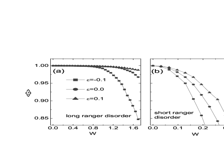
Figure 3 plots the sample-averaged two-terminal conductance as a function of the effective disorder strength for three different Fermi energies =-0.1, 0, 0.1, respectively. The edge magnetization is set to be =0.6. Each data point represents average over 20,000 sample configurations. Panel (a) is for the long range disorder case. We observe that, for all the three Fermi energies, the averaged conductances are robust against weak disorders, i.e. when 0.8, all the conductances are exactly quantized to be one in units of without conductance fluctuation. When 0.8, we find that of =-0.1 is quickly destroyed first, and that of =0.1 is the most robust one. This can be explained from the band structure shown in Fig. 2(b). One can see that the two edge states for a fixed Fermi energy have a large momentum separation when the Fermi energy is near the upper band bottom (e.g. =0.1). The separation decreases when the Fermi energy is approaching the valence band top (e.g. =-0.1). The large momentum separation (on the scale of valley separation) suppresses the long range impurity scattering which allows only small momentum transfer. Panel (b) shows the averaged conductance as a function of the short range nonmagnetic disorders, with other parameters being the same as that in panel (a). We find that the edge states are very sensitive to the disorders and therefore easily destroyed by small disorder strengths. We also performed calculations for magnetic disorders (not shown here) and the results are similar. Therefore, we conclude that our valley associated spin-polarized edge modes are robust against smooth disorder scattering.
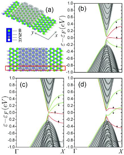
First Principles Calculations.— So far, we have investigated the spin-polarized edge modes in a graphene nanoribbon model Hamiltonian with a staggered sublattice potential, and an edge-specific spin polarization put in by hand. In the following, from first principles calculations, we provide a concrete system for the realization of our models by placing a zigzag-edged graphene nanoribbon on top of a hexagonal Boron-Nitride substrate. In our calculations, we set the lattice constant to be , and inter-layer distance AbinitioB6N6 . Figure 4.(a) illustrates the schematic configuration of the system. Here, we use () to label the width of graphene (Boron nitride), and . The single-layer graphene and Boron nitride are stacked with Nitrogen atoms on top of the hollow position. All the outer-most atoms are saturated with Hydrogen atoms, and we use the experimental values of the bond lengths: (B-H), (N-H), and (C-H). The self-consistent ground state calculations were performed within the non-equilibrium Green’s function coupled with the density-functional theory scheme Jeremy , and the local density approximation exchange-correlation potential (LDA-PZ81) was usedLDA_PZ81 .
In our calculations, we set , and . Panels (b) and (c) plot the band structures with spin anti-parallel/parallel configurations at the two zigzag boundaries. The grey region shows bulk band structure region (when both and approach infinity): a bulk gap around is opened, which is slightly larger than using VASP packageAbinitioB6N6 . In panel (b), we find that only the spin-up polarized edge states lie inside gap, which resembles the band structure of the tight-binding model. A small splitting in the figure is due to the interaction between the states with the same spin on the two boundaries, and will decrease along with the increasing system width. In panel (c), we observe that both the spin-up and spin-down states coexist in the gap. From both panels (b) and (c), one can obtain that the magnetization of each outermost carbon atom is about =. As shown in panel (d), one can apply an external transverse bias across the ribbons Louie to separate the mixed states and leave only the spin-down edge state in the bulk gap, which provides an efficient way to manipulate the spin-polarized edge states.
Conclusion.— We investigate on the edge modes of zigzag-edged graphene nanoribbons in the presence of a staggered sublattice potential. We find that the edge states form spin-polarized conducting channels which are robust against smooth impurity potentials. Using first principles calculation methods, we provide a specific system which exhibits such spin-polarized edge modes by placing the zigzag-edged graphene nanoribbons on top of a hexagonal Boron-Nitride substrate. The realization of this valley associated spin-polarized edge modes will enable the application of the graphene-based spintronics and valleytronics devices.
Z.Q. was supported by NSF (DMR0906025) and Welch Foundation (F-1255). Q.N. was supported by DOE (DE-FG02-02ER45958, Division of Materials Science and Engineering) and Texas Advanced Research Program. Y.Y. was supported by NSF of China (Grants No. 10974231) and the MOST Project of China (Grants No. 2007CB925000, and 2011CBA00100).
References
- (1) D. J. Thouless, M. Kohmoto, P. Nightingale, and M. denNijs, Phys. Rev. Lett. 49, 405 (1982).
- (2) Y. Hatsugai, Phys. Rev. Lett. 71, 3697 (1993).
- (3) C. L. Kane, and E. J. Mele, Phys. Rev. Lett. 95, 226801 (2005).
- (4) Q. Niu, and D. J. Thouless, J. Phys. A: Math. Gen. 17, 2453 (1984).
- (5) C. L. Kane, and E. J. Mele, Phys. Rev. Lett. 95, 146802 (2005).
- (6) W. Yao, S. A. Yang, and Q. Niu, Phys. Rev. Lett, 102, 096801 (2009).
- (7) Y. W. Son, M. L. Cohen, and S. G. Louie, Nature, 444, 347 (2006).
- (8) K. A. Ritter and J. W. Lyding, Nature Mater. 8, 235 (2009).
- (9) L. Jiao, L. Zhang, X. R. Wang, G. Diankov, H. J. Dai, Nature(London), 458, 877 (2009); D. V. Kosynkin, A. L. Higginbotham, A. Sinitskii, J. R. Lomeda, A. Dimiev, B. K. Price, J. M. Tour, Nature(London), 458, 872 (2009).
- (10) L. C. Campos, V. R. Manfrinato, J. D. Sanchez-Yamagishi, J. Kong, and P. Jarillo-Herrero, Nano Lett. 9, 2600 (2009).
- (11) X. Jia, M. Hofmann, V. Meunier et al., Science, 323, 1701 (2009); Ç. Ö. Girit, J. C. Meyer, R. Erni et al., Science, 323, 1705 (2009).
- (12) K. S. Novoselov, A. K. Geim, S. V. Morozov, D. Jiang, Y. Zhang, S. V. Dubonos, I. V. Grigorieva, and A. A. Firsov, Science, 306, 666 (2004); Y. B. Zhang, Y.-W. Tan, H. L. Stormer, and Philip Kim, Nature (London), 438, 201 (2005).
- (13) C. W. J. Beenakker, Rev. Mod. Phys. 80, 1337 (2008); A. H. Castro Neto, F. Guinea, N. M. R. Peres, K. S. Novoselov, and A. K. Geim, Rev. Mod. Phys. 81, 109 (2009).
- (14) J. Jung et al., Phys. Rev. Lett, 102, 227205 (2009); J. Jung et al., Phys. Rev. B, 79, 235433 (2009); J. Zhou et al., Nano Lett. 9, 3867 (2009); L. Yang et al., Phys. Rev. Lett., 101, 186401 (2008).
- (15) C. G. Tao, L. Y. Jiao, O. V. Yazyev et al., cond-mat/1101.1141.
- (16) F. Miao, S. Wijeratne, Y. Zhang, U. C. Coskun, W. Bao, C. N. Lau, Science, 317, 1530 (2007); Y. Y. Zhang, J.-P. Hu, X. C. Xie, W. M. Liu, Physica B, 404, 2259 (2007).
- (17) K. Wakabayashi, Y. Takane, M. Yamamoto, and M. Sigrist, New J. Phys., 11, 095016 (2009).
- (18) D. Xiao, W. Yao, and Q. Niu, Phys. Rev. Lett., 99, 236809 (2007).
- (19) This can be obtained through the Fourier transformation, and we have further numerically verified it.
- (20) Z. H. Qiao, J. Wang, Y. D. Wei, and H. Guo, Phys. Rev. Lett., 101, 016804 (2008).
- (21) S. Datta, Electronic Transport in Mesoscopic Systems (Cambridge University Press, Cambridge, UK, 2003).
- (22) M. P. López-Sancho, J. M. López-Sancho, and J. Rubio, J. Phys. F 14, 1205 (1984); 15, 851 (1985).
- (23) J. Taylor, H. Guo, and J. Wang, Phys. Rev. B, 63 245407 (2001); Phys. Rev. B, 63 121104 (2001).
- (24) J. P. Perdew, and A. Zunger, Phys. Rev. B, 23, 5048 (1981).
- (25) G. Giovannetti, P. A. Khomyakov, G. Brocks, P. J. Kelly, and J. van den Brink, Phys. Rev. B, 76, 073103 (2007).