Single-layer metallicity and interface magnetism of epitaxial graphene on SiC(000)
Abstract
We perform density functional theory calculations for the determination of the structural and electronic properties of epitaxial graphene on 4H-SiC(000). Using commensurate supercells that minimize non-physical stresses we show that, in contrast with Si-face epitaxial films, the first graphene layer that forms on the C-face of SiC is purely metallic with its -bands partially preserved. Typical free-standing characteristics are fully recovered with a second graphene layer. We moreover discuss on the magnetic properties of the interface and the absence of Fermi-level pinning effects that could allow for a plausible device operation starting from the off-state.
Epitaxial graphene has emerged as a highly attractive system for device integration by providing a combination of characteristics that constitute a significant advantage with respect to competitive graphene production technology: wafer size scales2009NatMa…8..203E and direct growth on semi-insulating substrates. The process is based on the sublimation of Si atoms starting from SiC substrates in ultra high vacuum or ambient pressure furnaces2009NanoL…9.2605J . Accurate control of the growth parameters can allow for the reformulation of graphene films from the remaining C surface atoms. The structural, electronic and transport properties of epitaxial graphene strongly depend on the the polarization of the SiC surface: Si-face epitaxial graphene (i.e. graphene on SiC(0001)) is characterized by the formation of a first carbon-rich interface layer with a surface reconstruction, over which Bernel stacked graphene layers grow. Interface interaction imposes significant -type doping while scatterers reduce mobility values with respect to the -deposited case2009NatMa…8..203E . Typical graphene characteristics (e.g. the half-integer quantum hall effect) are recovered by the application of a gate voltage that lowers the Fermi level around the Dirac point2010PhRvB..81s5434J . C-face epitaxial graphene (i.e. graphene on SiC(000)) is subject to a less stringent rotational ordering with respect to the substrate2010arXiv1001.3869S ; 2009JPCM…21m4016S whereas the presence of an interface buffer layer, although predicted by theoretical calculations2007PhRvL..99g6802M ; 2007PhRvL..99l6805V , is still a matter of debatecamara:093107 ; 2007PhRvB..75u4109H ; 2009PhRvB..80w5429H ; 2009JPCM…21m4016S . A complex rotational symmetry of subsequent graphene layers other than the AB stacking sequence is present 2010arXiv1001.3869S that allows for the manifestation of single-layer properties even in the case of a multilayer structure2009PhRvL.103v6803S . C-face monolayers show higher mobilities with respect to the (0001) case and the typical half-integer quantum hall effect at low temperaturescamara:093107 ; 2009ApPhL..95v3108W . Doping is also present here, however controversy holds over the type and the concentration of carriers2010PhRvL.104m6802S ; camara:093107 ; 2009ApPhL..95v3108W .
In this article we focus on C-face epitaxial graphene by means of density functional theory calculations. Starting from a basis of lattice commensuration for graphene and the SiC substrate, we show that results can significantly differ with respect to non-commensurate models2007PhRvL..99g6802M ; 2007PhRvL..99l6805V . Contrary to the Si-face2009ApPhL..95f3111D , we find that the first graphene layer preserves a purely metallic character with a complete absence of a bandgap, while partially maintaining its -bands. However, interaction with the substrate perturbs the typical Dirac cone that only appears with the addition of a second graphene layer. We moreover show the presence interface ferromagnetism due to strong exchange interactions and an absence of the Fermi-level pinning effects previously reported for (0001) films2009ApPhL..95f3111D ; 2009PhRvB..80x1406S ; ouerghi:161905 .

We perform ab initio calculations based on the Density Functional Theory (DFT) within the Local Spin Density Approximation (LSDA) as implemented in the SIESTA computational code2002JPCM…14.2745S . The 4H-SiC epitaxial graphene structures comprise of four bilayers of a () SiC substrate (passivated with H at the bottom) over which single and double layers of graphene grow, forming a () supercell that satisfies lattice commensuration and minimizes non-physical stresses (Calculated lattice constants: Å, Å). Contrary to reconstructions, here there exists no rotational angle for the graphene supercell with respect to the SiC substrate. Such a configuration is often observed in experiments for (000) samples2010arXiv1001.3869S . A basis set of double- valence (plus polarization) orbitals has been used for C (Si) and H, along with Troulier-Martins pseudopotentials1991PhRvB..43.1993T for the modeling of ionic cores. Both basis set sensitivity and pseudopotentials have been tested to accurately reproduce the bandstructure of hexagonal SiC polytypes and graphene. Sampling of the Brilouin zone takes place by a Monhorst-Pack grid, whereas bandstructure is plotted for 130 nonequivalent -points along the closed path. A mesh cutoff energy of 500 Ry has been imposed for real-space integration, while structures have been relaxed until forces were less than 0.04 eV/Å.

At the end of the relaxation process, the first graphene layer presents a corrugation with thickness Å (Fig. 1(a)) and has structural characteristics that present some fundamental differences with respect to the buffer layer of the non-commensurate reconstruction2007PhRvL..99g6802M ; 2007PhRvL..99l6805V . A periodic reproduction of the unit cell (Fig. 1(b)) shows the presence of small islands covering almost the four fifths of the epilayer surface that strongly maintain -bonding characteristics and represent the areas of the honeycomb lattice that are more distant from the substrate ( Å). Below these islands the substrate relaxes in an ideal surface reconstruction of the C-face2010JPCM…22z5003W where also substrate carbon atoms strongly hybridize. Substrate reconstruction is the origin of the energetic stability of this structure: we have calculated that the ground state energy proposed by our model is significantly lower than the one of the case. The islands of the epilayer are terminated by carbon atoms that strongly bond with the substrate and loose the hybridization for the one. From a modeling point of view, the increase of the lattice periodicity for this supercell with respect to the one is in favor of bonding. Indeed, the biggest part of carbon atoms that form the graphene epilayer maintain their orbitals and only few atoms covalently bond with the substrate. It should be moreover noted that in this geometrical configuration stresses are minimized, since the bonds of the graphene layer have a mean distance of Å whereas interface ones relax at Å, which slightly exceeds that of pure diamond. Moreover, interesting structural comparisons between the present calculations and the scanning tunneling microscopy images of Refs. 10; 5 for monolayer graphene grown on SiC (000)() can be made (e.g. see figure 1(b) of the present manuscript and figure 2(d) of Ref. 10).

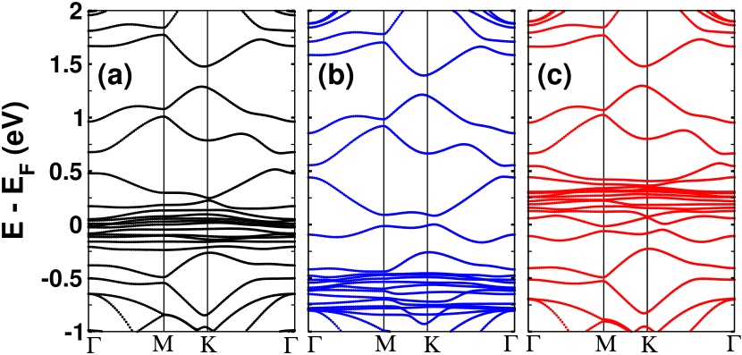
Fig. 2 shows the electronic bandstructure of the first graphene layer on 4H-SiC(000). The key aspect of this interaction is that the monolayer preserves a purely metallic character with its bands prevailing within the SiC-substrate bandgap, in consistency with electrical measurements on C-face monolayers2009PhRvB..80w5429H . This feature is in a clear contrast with the carbon-rich layer grown on the Si-face2007PhRvL..99l6805V . However, the interaction with the substrate, notwithstanding weak, perturbs the Dirac cone and the bands do not preserve the typical linearity of free-standing graphene near the Fermi level. A careful view of the spin-polarized bandstructure (Fig. 2(b-c)) that corresponds to the most stable electronic configuration shows some important differences with respect to the spin-unpolarized one (Fig. 2(a)). The presence of quasi-flat bands near the Fermi level of this system derives from SiC surface and is localized on C atoms that are not bound to the graphene epilayer. From the spin-unpolarized bandstructure one can deduce that these states pin the Fermi level at the interface as similarly calculated for Si-face grown graphene2009ApPhL..95f3111D (where this phenomenon is argued to be one of the main factors for the strong -type doping of that system2009PhRvB..80x1406S ; ouerghi:161905 ). However the spin-polarized bandstructure shows a different picture: here the surface states are half-filled and strong exchange interactions make them split above and below the Fermi level by , leaving the graphene/4H-SiC(000) system unpinned (in agreement with previous calculations of Ref. 6).
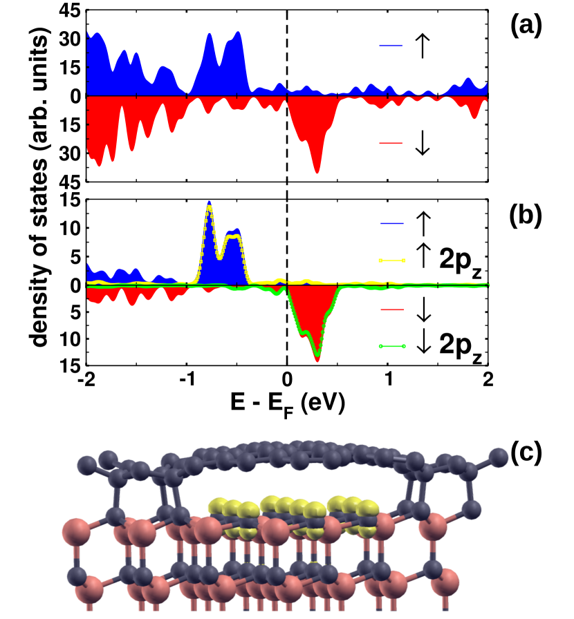
The presence of significant exchange interactions makes necessary a more careful analysis of magnetism issues in the interface of these systems. Fig. 3 shows spin-up () and spin-down () density of states (DOS) and electronic density configurations for the graphene/4H-SiC(000) system. The total density of states (Fig. 3(a)) reveals the presence of a big concentration of spin-up states from to below the Fermi level, and similarly for spin-down states from to above the Fermi level. A careful analysis of the projected density of states on the carbon atoms of the first SiC bilayer below the graphene layer (Fig. 3(b)) shows that a major component of these two peaks derives from the those carbon atoms that are not covalently bonded with the graphene overlayer. Moreover, the contributions of the orbitals are almost exclusive in these peaks (the remaining DOS contributed by orbitals that can be found in the system is localized at the graphene monolayer). The surface and band-splitting gives rise to local magnetization phenomena at the heterostructure’s interface (Fig. 3(c)) where a ferromagnetic order is present. C substrate atoms that are not covalently bound with the epilayer have magnetic moments that range within , whereas those covalently bound are not magnetic. Magnetism holds only for the first bilayer of the substrate and rapidly decreases with distance: the third SiC bilayer and the graphene epilayers are not magnetic. Interface magnetism however influences the electronic bands of the graphene epilayer where a shift of between and bands can be observed (Fig. 2(b) and 2(c)).

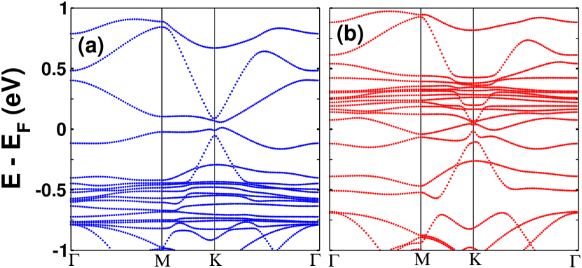
As in the case of (0001) epitaxy, typical free-standing graphene characteristics and the presence of the Dirac cone are recovered with the second graphene layer (Fig. 4). This layer interacts weakly with the first epilayer, maintaining a mean distance that is similar to that of Bernel-stacked graphite and shows a smaller corrugation with a layer thickness Å, in accordance with measurements2007PhRvB..75u4109H . It should be again noted here that the Fermi level remains unpinned by the interface and is purely determined by the position of the Dirac cone.
To conclude, in this study we have presented ab initio electronic structure calculations for monolayer and bilayer epitaxial graphene systems grown on 4H-SiC(000). Contrary to epitaxial graphene on SiC(0001), the first graphene layer that grows on the C-face of SiC maintains a purely metallic character and an important presence of electrons along with a non-negligible coupling with the substrate. The particularity of its geometrical configuration consists in a corrugated surface where small -bonded islands are terminated by carbon atoms that covalently bind to the substrate. Below these islands also the surface carbon atoms -hybridize, while their bands are half-filled and present a ferromagnetic order due to the presence of strong electron exchange interactions. Typical graphene-like characteristics are recovered with the addition of a second graphene layer. According to this picture C-face epitaxial graphene should maintain some important advantages with respect to the Si-face one, like the absence of a Fermi-level pinning effect that could allow for a plausible device operation starting from an off-state. In this sense, doping effects measured in the laboratory2009ApPhL..95v3108W should likely be attributed to environmental or local disorder factors like the presence of impurities, rather than considered as an intrinsic characteristic of the interface. Methodologically, this study argues that approaches that go beyond the reconstruction2010PhRvB..82l1416P are fundamental for the correct modeling of graphene on SiC(000).
The authors would like to acknowledge the European Science Foundation (ESF) under the EUROCORES Program EuroGRAPHENE CRP GRAPHIC-RF for partial financial support. Computations have been performed at the CINECA supercomputing facilities under project TRAGRAPH.
References
- (1) K. V. Emtsev, A. Bostwick, K. Horn, J. Jobst, G. L. Kellogg, L. Ley, J. L. McChesney, T. Ohta, S. A. Reshanov, J. Röhrl, E. Rotenberg, A. K. Schmid, D. Waldmann, H. B. Weber, and T. Seyller, Nature Materials 8, 203 (Mar. 2009).
- (2) G. G. Jernigan, B. L. Vanmil, J. L. Tedesco, J. G. Tischler, E. R. Glaser, A. Davidson, III, P. M. Campbell, and D. K. Gaskill, Nano Letters 9, 2605 (Jul. 2009).
- (3) J. Jobst, D. Waldmann, F. Speck, R. Hirner, D. K. Maude, T. Seyller, and H. B. Weber, Physical Review B 81, 195434 (May 2010).
- (4) M. Sprinkle, J. Hicks, A. Tejeda, A. Taleb-Ibrahimi, P. Le Fèvre, F. Bertran, H. Tinkey, M. C. Clark, P. Soukiassian, D. Martinotti, J. Hass, and E. H. Conrad, Journal of Physics D: Applied Physics 43, 374006 (2010).
- (5) U. Starke and C. Riedl, Journal of Physics Condensed Matter 21, 134016 (Apr. 2009).
- (6) A. Mattausch and O. Pankratov, Physical Review Letters 99, 076802 (Aug. 2007).
- (7) F. Varchon, R. Feng, J. Hass, X. Li, B. N. Nguyen, C. Naud, P. Mallet, J. Veuillen, C. Berger, E. H. Conrad, and L. Magaud, Physical Review Letters 99, 126805 (Sep. 2007).
- (8) N. Camara, B. Jouault, A. Caboni, B. Jabakhanji, W. Desrat, E. Pausas, C. Consejo, N. Mestres, P. Godignon, and J. Camassel, Applied Physics Letters 97, 093107 (2010).
- (9) J. Hass, R. Feng, J. E. Millán-Otoya, X. Li, M. Sprinkle, P. N. First, W. A. de Heer, E. H. Conrad, and C. Berger, Physical Review B 75, 214109 (Jun. 2007).
- (10) F. Hiebel, P. Mallet, L. Magaud, and J. Veuillen, Physical Review B 80, 235429 (Dec. 2009).
- (11) M. Sprinkle, D. Siegel, Y. Hu, J. Hicks, A. Tejeda, A. Taleb-Ibrahimi, P. Le Fèvre, F. Bertran, S. Vizzini, H. Enriquez, S. Chiang, P. Soukiassian, C. Berger, W. A. de Heer, A. Lanzara, and E. H. Conrad, Physical Review Letters 103, 226803 (Nov. 2009).
- (12) X. Wu, Y. Hu, M. Ruan, N. K. Madiomanana, J. Hankinson, M. Sprinkle, C. Berger, and W. A. de Heer, Applied Physics Letters 95, 223108 (Nov. 2009).
- (13) D. Sun, C. Divin, C. Berger, W. A. de Heer, P. N. First, and T. B. Norris, Physical Review Letters 104, 136802 (Apr. 2010).
- (14) I. Deretzis and A. La Magna, Applied Physics Letters 95, 063111 (Aug. 2009).
- (15) S. Sonde, F. Giannazzo, V. Raineri, R. Yakimova, J. Huntzinger, A. Tiberj, and J. Camassel, Physical Review B 80, 241406 (Dec. 2009).
- (16) A. Ouerghi, R. Belkhou, M. Marangolo, M. G. Silly, S. E. Moussaoui, M. Eddrief, L. Largeau, M. Portail, and F. Sirotti, Applied Physics Letters 97, 161905 (2010).
- (17) J. M. Soler, E. Artacho, J. D. Gale, A. García, J. Junquera, P. Ordejón, and D. Sánchez-Portal, Journal of Physics Condensed Matter 14, 2745 (Mar. 2002).
- (18) N. Troullier and J. L. Martins, Physical Review B 43, 1993 (Jan. 1991).
- (19) J. Wang, L. Zhang, Q. Zeng, G. L. Vignoles, and L. Cheng, Journal of Physics Condensed Matter 22, 265003 (Jul. 2010).
- (20) O. Pankratov, S. Hensel, and M. Bockstedte, Physical Review B 82, 121416 (2010).