Optical Conductivity and Electronic Structure of CeRu4Sb12 under High Pressure
Abstract
Optical conductivity [] of Ce-filled skutterudite CeRu4Sb12 has been measured at high pressure to 8 GPa and at low temperature, to probe the pressure evolution of its electronic structures. At ambient pressure, a mid-infrared peak at 0.1 eV was formed in at low temperature, and the spectral weight below 0.1 eV was strongly suppressed, due to a hybridization of the electron and conduction electron states. With increasing external pressure, the mid-infrared peak shifts to higher energy, and the spectral weight below the peak was further depleted. The obtained spectral data are analyzed in comparison with band calculation result and other reported physical properties. It is shown that the electronic structure of CeRu4Sb12 becomes similar to that of a narrow-gap semiconductor under external pressure.
1 Introduction
Physical properties of materials under external pressure have attracted much interest recently.[1] By applying a hydrostatic pressure, one may reduce the interatomic distance in a material, and therefore can tune its physical properties in a continuous manner. In addition, the pressure technique does not introduce any disorder into the crystal lattice, unlike the case of chemical alloying. Various novel properties such as a superconductivity [2], a transition/crossover between localized and delocalized states[3], and quantum critical transitions[4] have been explored under external pressure. It is interesting to experimentally examine the electronic structures associated with these pressure-induced phenomena. Infrared (IR) spectroscopy technique is very useful in this regard, since it can give the optical conductivity [] of a sample loaded in a pressure generating cell. contains much information about the microscopic electronic structures near the Fermi level. Note that the other common spectroscopic techniques such as photoemission and tunneling spectroscopies are technically difficult to perform with a pressure cell. In this work, we apply the high pressure IR technique to CeRu4Sb12.
CeRu4Sb12 is one of the compounds with the “filled skutterudite” crystal structure, which have attracted a great amount of attention due to their interesting physical properties.[5] In the case of Ce-filled skutterudites Ce, the reported physical properties are widely varied depending on the constituent atoms and . For =P and As, the compounds studied so far (=Fe, Ru, and Os) all show semiconductor-like properties with the estimated energy gaps ranging from 5-10 meV for As compounds[6, 7] to 40-130 meV for P compounds.[8, 9, 10] For =Sb, in contrast, physical properties for the three compounds with =Fe, Ru, and Os show more metallic characteristics. In particular, CeRu4Sb12 shows some anomalous and interesting properties.[11, 12, 13, 14, 15] The electrical resistivity () of CeRu4Sb12 rapidly decreases at low temperature () below 100 K, and its electronic specific heat coefficient is moderately enhanced, 80 mJ/K2mol. These properties are characteristic of intermediate valence Ce compounds. In addition, pronounced non-Fermi liquid properties were observed below 4 K.[11] Under external pressure, of CeRu4Sb12 below 100 K was found to markedly increase. At 8 GPa, the data suggested an energy gap of a few meV,[14, 15] and it showed further increases at 10 GPa.[15] The optical conductivity of CeRu4Sb12 in the IR range has also been studied at ambient pressure.[16, 17, 18] showed a strong suppression below 0.1 eV at low ,[16, 17] with the tail of a narrow Drude response due to heavy electron state.[18]
In this work, in order to probe the pressure evolution of electronic structures in CeRu4Sb12, we have derived its at pressures up to 8 GPa. The infrared data are analyzed in comparison with the band calculation result and other published physical properties. It is shown that the electronic structures of CeRu4Sb12 indeed becomes similar to that of a semiconductor under high pressure.
2 Experimental
The samples of CeRu4Sb12 used in this work were single crystals grown with self-flux method.[13] spectra in vacuum were obtained from the measured optical reflectance spectra []. in vacuum were measured under near-normal incidence configuration between 7 meV and 30 eV, as previously discussed in detail.[20, 19] The Kramers-Kronig (KK) analysis was used to derive from the measured data, where the low-energy range below the measurement limit was extrapolated with a Hagen-Rubens function.[21, 22] For high pressure measurements, an external pressure was applied with a diamond anvil cell (DAC), as previously described.[3, 23] In a DAC, a mechanically polished surface of a sample with approximately 200 200 30 m3 dimensions was closely attached to the culet face of a diamond anvil (See also Fig. 8(a) in the Appendix.) The diameter of the culet face was 800 m. The diamond anvils were of type IIa with low density of impurities, which is crucial for infrared studies.[23] The pressure transmitting medium used was glycerin, which has been shown to have good characteristics as a pressure transmitting medium.[24] The of the sample was measured relative to a gold film mounted together with the sample in DAC [see also Fig. 8(a)]. To measure of a small sample under such a restricted condition, synchrotron radiation (SR) was used as a bright IR source at the beam line BL43IR of SPring-8.[25] For high pressure data, Drude-Lorentz fitting analyses were used to derive from measured , as discussed later. More technical details of the high pressure measurement with DAC and IR SR can be found elsewhere.[23]
3 Results and Discussion
For technical reasons, high pressure measurements of with DAC were done with mechanically polished surfaces, rather than with as-grown surfaces. In the course of this study, we have realized that measured on a polished surface of CeRu4Sb12 exhibit noticeable differences from previous data measured on as-grown surfaces.[16, 17] Therefore, we will first describe and data measured on both polished and as-grown surfaces, then will discuss the results of high pressure experiment.
3.1 and measured in vacuum with polished and as-grown surfaces
Figures 1(a) and 1(b) compare the and spectra of CeRu4Sb12 measured on mechanically polished and as-grown surfaces, respectively, in vacuum. The spectra were derived from the measured using the KK analysis.
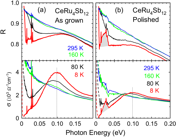
The strong dependences of and have been already discussed in detail for as-grown cases.[16, 17] They result from the formation of a conduction (c)- electron hybridized state. Here, important features are the formation of a mid-IR peak in at 0.1 eV and the depletion of below the mid-IR peak energy. The latter feature makes of CeRu4Sb12 appear like that of an insulator. However, CeRu4Sb12 shows metallic characteristics in its transport and magnetic properties at low . There is a narrow, -function-like Drude component due to heavy-mass carriers below the measurement range of this study.[18] Such a spectrum consisting of a narrow Drude component, a depletion of spectral weight (pseudogap), and a mid-IR peak have been observed for many intermediate-valence Ce and Yb compounds.[19, 26, 27, 28, 29] It has been shown that the mid-IR peak energies observed for various Ce compounds are roughly proportional to their - hybridization energies estimated with specific heat data and the single-ion Anderson model.[16, 27, 28] The spectral shapes of our data for the as-grown case in Fig. 1(a) agree well with those reported by Dordevic et al..[16, 18]
The spectra of the polished surface in Fig. 1(b) are basically similar to those of the as-grown one in Fig. 1(a), but there are some noticeable differences. Most significant is that the optical phonon peaks for the as-grown case, seen below 40 meV, are much sharper and better resolved than the polished case. In the polished case, there is a broad band, indicated by the gray area in Fig. 1(b), superimposed on the narrower phonon lines. The peak positions of the narrow phonon lines, however, have only small differences (less than 2 cm-1) between the two cases. The most likely origin for the broad band is a slight disorder in the crystal lattice induced by polishing. The disorder may have relaxed the momentum conservation rule for a phonon creation by a photon, causing the phonon band in Fig. 1(b) due to many phonon modes that are forbidden without disorder. Nevertheless, the spectra at low of polished case well preserves the main features in of the as-grown sample, namely the appearance of the mid-IR peak with the spectral depletion with cooling. Therefore the data obtained from a polished sample should be valid for the discussion of electronic structures in CeRu4Sb12 under pressure. All the results presented hereafter are based on polished samples.
3.2 measured under high pressure with DAC
In a DAC, is measured at a sample/diamond interface, rather than the usual sample/vacuum interface. It should be noted that the refractive index of diamond, 2.4, is much larger than that of vacuum. According to Fresnel’s formula, at an interface between a material and a transparent medium is expressed as:[21, 22]
| (1) |
Here, and are the real and imaginary parts of the complex refractive index of the material, respectively, and is the (real) refractive index of the medium, =2.4 for diamond and 1.0 for vacuum. Hereafter, we denote relative to vacuum as , and that relative to diamond as . Figures 2(a)-2(c) compare measured , expected from , and actually measured in DAC at a low pressure of 0.2 GPa, respectively.
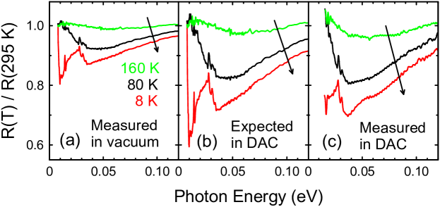
To calculate of Fig. 2(b), and were first derived from the KK analysis of a spectrum, and were substituted into Eq. (1) with =2.4 to obtain . This was repeated for spectra measured at different ’s. To highlight their dependences, the spectra in Figs. 2(a)-2(c) have been normalized by those at 295 K. It is clear that the corresponding spectra in Figs. 2(b) and 2(c) agree with each other reasonably well.
Figure 3 shows spectra measured at external pressure of 0, 4, and 8 GPa.
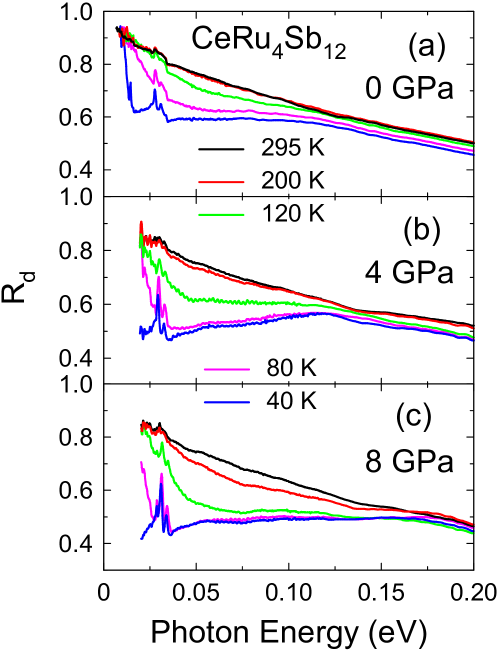
In the present study, was measured with varying at fixed pressures of 4 and 8 GPa, rather than with varying pressure at fixed , since it was technically difficult with our gas-driven DAC to vary the pressure up to 8 GPa at low . spectra at 0 GPa in Fig. 3(a) are derived from via KK analysis, as already discussed for the spectra in Figs. 2(a) and 2(b). The spectra at 4 and 8 GPa in Figs. 3(b) and 3(c) were obtained as follows. The reflectance spectra above 70 meV were actually measured in DAC. Those below 70 meV, i.e., the far IR range, were obtained by multiplying the spectra at 0 GPa in Fig. 3(a) by the relative changes of with pressure and temperature measured in DAC. This procedure for the far IR range was taken because it was technically difficult to accurately determine the absolute value of the reflectance in DAC, due to diffraction effects of long wavelength far-IR range. The uncertainty in the magnitude of the overall under high pressure is estimated to be 2 %. Figure 3 clearly shows that, with increasing pressure, the depletion of with cooling becomes larger, and occurs over a wider photon energy.
3.3 derived from measured at high pressures
To obtain the optical conductivity from the spectra measured in DAC, we have used Drude-Lorentz (DL) spectral fitting of rather than the KK analysis. The DL fitting was used rather than the KK analysis because the present study with DAC is performed only over a limited energy range (below 1.1 eV), although a KK analysis generally requires a wider spectral range. In addition, it is difficult with KK analysis to take into account multiple reflections within a thin layer of pressure medium, that was present between the sample and diamond. All the details of the DL fitting procedure and the analysis of multiple reflections are described in the Appendix, with a list of the obtained fitting parameters and examples of actual fittings. Here we present the obtained spectra only.
Figure 4 shows the obtained spectra of CeRu4Sb12.
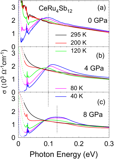
The spectra at 0 GPa in (a) were obtained from with K-K analysis, and those at 4 and 8 GPa in (b) and (c) were obtained from measured with the DL fitting. From the data, the evolution of at high pressure appears qualitatively similar to those at zero pressure. Namely, a mid-IR peak develops with cooling, and the spectral weight at the lower-energy side of the peak is progressively depleted with cooling. However, under pressure, the development of the mid-IR peak starts at higher . For example, at 0 GPa there is no mid-IR peak at 200 K yet, but at 8 GPa, it is already observed at 200 K. In addition, the mid-IR peak apparently shifts to higher energy with pressure, as indicated by the vertical broken lines in Fig. 4, from about 0.1 eV at 0 GPa to 0.13 eV at 8 GPa. Figure 5 plots the mid-IR peak energies versus , which confirms the above observations.
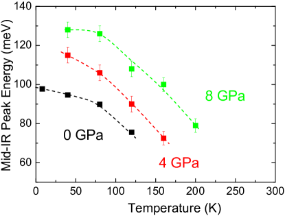
Furthermore, Fig. 4 shows that the spectral depletion below the mid-IR peak energy becomes much more pronounced at higher pressure. Combined with our previous finding that the mid-IR peak energy is scaled with the - hybridization energy,[28] the present result indicates that the - hybridization energy actually increases with external pressure. Although this property in Ce compounds has been widely assumed on the basis of transport and magnetic properties measured under external pressure, this is the first, direct spectroscopic evidence for the property.
In addition to the mid-IR peak, a shoulder at 25 meV has been observed in of CeRu4Sb12.[16] Namely, below 25 meV decreased rapidly with cooling below 80 K, in addition to the overall decrease of below the mid-IR peak. This shoulder is also seen in Fig. 1(a), although it is not clear due to the overlapping phonon peaks. Similar shoulder has been observed in of many other Ce and Yb compounds,[20, 30, 31] and its relation to - hybridization state has been discussed. Although the pressure evolution of this shoulder would be quite interesting, its energy (25 meV) was close to the low-energy limit of our study (20 meV), and it was difficult to follow the pressure evolution.
3.4 Analysis of the absorption edge
The spectrum at 40 K and 8 GPa shows a strong depletion of spectral weight below the mid-IR peak energy. It is indeed very similar to that of a narrow-gap semiconductor having a small energy gap and a low density of free carriers. However, unlike the case of an ideal band semiconductor,[22, 32] in Fig. 4 does not show a clear onset, and the energy gap magnitude is unclear. The lack of a clear onset may be partly due to the nature of Lorentz function itself, since, by definition, it goes through the origin. Therefore, to examine the onset of absorption, here we employ a technique originally used for indirect-gap semiconductors such as Ge,[32, 33] and also for Kondo semiconductors.[34, 31] Near the fundamental absorption edge at an indirect energy gap, it has been shown that the square root of the absorption coefficient is proportional to the photon energy relative to energy gap, namely ).[32] This dependence is due to indirect (phonon-assisted) excitation of electrons by photons.[32] Figure 6(a) plots of CeRu4Sb12 at 40 K and different pressures, and Figure 6(b) plots the corresponding for comparison.
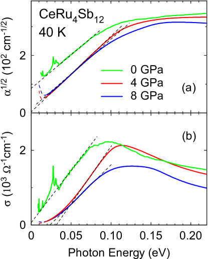
Here, at 0 GPa was obtained from the KK analysis of , while those at 4 and 8 GPa were derived from the results of DL fitting. First, note that at 40 K and 0 GPa, shows a linear energy dependence below 80 meV as indicated by the broken line. As mentioned above, this linear dependence may suggest light absorption due to indirect process. The intercept of the plot with the energy axis has a large negative value, which should correspond to the fact that CeRu4Sb12 at 0 GPa is a metal, without an energy gap. (Since the original model for indirect semiconductors[32, 33] assumed a positive intercept with the presence of a gap, the magnitude of this negative intercept should not have a physical significance.) Next, consider the high pressure data at 4 and 8 GPa. Since the nature of Lorentz function leads to a linear dependence in a plot, the linear dependences alone cannot prove the presence of indirect absorption. However, since such a behavior is already observed at 0 GPa without a fitting, it is quite reasonable to interpret the data as showing pressure-induced shifts of the linear portion already observed at 0 GPa. Then, note that the intercept of the linear portion (dotted line) is near the origin for both 4 and 8 GPa. This result may indicate that the overlap between the valence band (VB) and conduction band (CB) decreases with pressure, and that CeRu4Sb12 is close to a crossover to a semiconductor. But since the intercept is still near zero energy, there is no clear energy gap yet on the basis of the optical spectra. This appears consistent with the reported result of electrical resistivity.[14] Namely, a thermally activated dependence was observed at 8 GPa, but only with a small activation energy ( 2 meV) and only over a narrow range (20-40 K). Both the very small activation energy and its narrow range indicate that the energy gap has not fully opened yet. A pressure higher than 10 GPa may be needed to open a clear energy gap in CeRu4Sb12. The spectra in Fig. 6(b) also show a nearly linear dependence below the mid-IR peak energy, as indicated by the broken lines. The crossing of the linear portion with horizontal axis is located near the origin at 0 GPa, but it shifts to about 20 meV at 4 and 8 GPa. This result also suggests pressure shifts of absorption edge, although the linear dependence does not distinguish between indirect and direct gaps.
In contrast to the clear shift of mid-IR peak with pressure from 4 to 8 GPa in Fig. 4, the absorption edge seen in Fig. 6 shows almost no shift over the same pressure range. This results from a broadening of the mid-IR peak with pressure from 4 to 8 GPa. Although the significance of this result is unclear, the broadening probably corresponds to an increase of the bandwidth with pressure for the hybridized states near .
3.5 Electronic structures of CeRu4Sb12 with and without external pressure
At ambient pressure, CeRu4Sb12 shows typical properties of Ce-based intermediate-valence metals, with a rapid decrease of resistivity below 80 K and an electronic specific heat coefficient of about 80 mJ/K2mol.[11, 12] A Hall effect study showed that the majority carriers were the holes,[35] and a clear de Haas-van Alphen (dHvA) signal showed a Fermi surface with a cyclotron mass of about 5 .[36] These works have suggested that CeRu4Sb12 should be a semimetal with at least one hole pocket in the Fermi surface.
Figure 7(a) shows the band structure of CeRu4Sb12 calculated with local density approximation (LDA) and full-potential linearized augmented plane wave (FLAPW) method.[37] Only the vicinity of Fermi level () is shown, along the P--H line in the Brillouin zone.
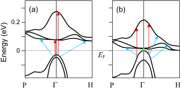
According to the calculation, [the broken line in Fig. 7(a)] does not cross any band, and hence CeRu4Sb12 should be an insulator with an energy gap of about 0.1 eV in the total DOS, between the top of VB at point and the bottom of CB at H point. In the CB, three flat bands are seen around P and H points, which originate from the Ce 4 =5/2 levels. The dome-shaped portion around of the top-most band is due to hybridized Sb state. The VB is mainly derived from the Sb , but the top of VB at has a strong mixing of Ce 4 state. In this situation, the energy gap of 0.1 eV in the total DOS should lead to a clear gap in with an onset at 0.1 eV, rather than the mid-IR peak at 0.1 eV as observed. [In the case of CeP12 (=Fe, Ru, Os),[38] an energy gap with an onset at 0.2-0.3 eV was actually observed ] To explain the above result and the metallic characteristics observed in other physical properties, we suggest that the actual band structure should be similar to that described in Fig. 7(b). In this suggested band structure, the flat -derived CB states have been moved closer to the VB states. Note that, although Fig. 7(b) is drawn as compensated semimetal, it is only intended as an illustration, assuming a stoichiometric composition. In experiments, only one Fermi pocket in the dHvA data[36] and a positive Hall coefficient[35] have been observed. These results may indicate a single hole pocket in an uncompensated semimetal. This may possibly result from a slight deviation of Ce filling from 100 %. But it has also been discussed that the electron pocket at H point, even if present, may be very small and may have a very large effective mass, resulting in the lack of corresponding dHvA signal and a positive Hall coefficient.[35, 36]
In Figs. 7(a) and 7(b), the vertical (red) and oblique (blue) arrows indicate the direct (momentum conserving) and indirect (phonon-assisted) optical transitions, respectively, which may occur in this band structure and may contribute to the mid-IR peak in . In particular, the indirect ones at low energy range suggested by the data in Fig. 6(a) may have actually resulted from such transitions as in Fig. 7(b). In this case, however, direct transitions from the top of VB to the low-lying, -derived CB around point, shown by the short vertical (green) arrow in Fig. 7(b), do not seem to have contributed to the observed . This is because, if they strongly contribute, would have much stronger spectral weight below 0.1 eV. One possible reason for such “dark” transitions is that the states near the top of VB should have strong mixture of 4 component, and the transitions such as that indicated by the short vertical (green) arrow in Fig. 7(b) have a strong - character: The Bloch function of a given state should be a superposition of 4-derived component, , and other components, . Then the optical transition matrix element should consist of the terms , , and , where is a dipole operator. Since the - term is zero due to the parity selection rule,[22, 32] and since the transition shown by the short vertical (green) arrow in (b) should have a large fraction of such - transition, the transition probability may be also small. An effective band model based on a tight binding approximation[39, 40] was also employed to calculate of CeRu4Sb12 including electron correlation effects. By introducing a dispersion (broadening) of 4 electron level, a compensated semimetallic band structure was obtained.[40] This model did not include the 4 degeneracy, so that the obtained band structure did not have the low-lying, flat CB around of Fig. 7(a). This model nevertheless reproduced the observed qualitatively well, which may also suggest that the 4-derived flat bands near do not strongly contribute to .
Under pressure, it is theoretically expected in a Ce compound that the electron levels are shifted upward relative to . The CB states shown in Fig. 7 are under strong influence of hybridization between Ce 4 and Sb 5 states, and therefore it is expected that the CB states are also pushed upward by the pressure shift of 4 state. This may also reduce the overlap between VB and CB. The experimentally observed semiconductor-like characteristics of CeRu4Sb12 under pressure, namely the increase of resistivity, is most likely the result of this electron energy shift. This interpretation is also consistent with the results of Fig. 6, i.e., an increase in the onset energy of absorption and the upward shift of mid-IR peak in . The upward shift of 4 levels with pressure would also reduce the density of thermally populated carriers at low , which is consistent with the observed increase of resistivity under pressure.[14] If the pressure is further increased, the 4 level shift would eventually lead to the opening of a true energy gap in the total DOS, similar to the situation in Fig. 7(a). Note that in CeP12 and CeAs12, whose lattice constants are smaller than that of CeSb12, an energy gap is in fact observed.[6, 7, 8, 9, 10, 38]
4 Conclusion
The optical conductivity of Ce-filled skutterudite compound CeRu4Sb12 was measured at low temperatures under high pressure up to 8 GPa. With increasing pressure, the characteristic mid-IR peak in shifted toward higher energy. In addition, the depletion of below the mid-IR peak energy became more significant and well-developed. These results were discussed in comparison with other experimental results and band calculations. The observed evolution of with pressure indicates that the energy separation between the 4f-derived states above and below the Fermi level increases with pressure. The spectrum at 8 GPa is indeed similar to that of a narrow-gap semiconductor with a small density of residual carriers, which is consistent with the semiconductor-like behavior of resistivity with a small activation energy over a narrow range. However, on the basis of our optical data, an energy gap is not fully open yet at 8 GPa. A pressure greater than 10 GPa may be therefore needed to observe a clear gap opening. Such a higher pressure study is desired in future to further probe the electronic structures of CeRu4Sb12 under pressure.
5 Acknowledment
H. O. would like to thank Dr. H. Yamawaki for providing the gasket material used in the DAC. This work has been supported by the following Grants-In-Aid for Scientific Research from Ministry of Culture, Education, Science, Sports and Technology of Japan: Innovative Area “Heavy Electron” (21102512-A01) and Scientific Research B (17340096). Experiments at SPring-8 were performed under the approval by JASRI (2009B0089, 2009A0089, 2008B1070, 2008A1239).
6 Appendix
This Appendix describes the Drude-Lorentz fitting procedures used for deriving the optical conductivity from the spectra measured in DAC. Figure 8(a) illustrates the experimental condition in the present IR study. The fitting procedure takes into account effects of diamond refractive index and a thin layer of pressure medium which is present between the diamond and sample. These are described in detail below.
6.1 Drude-Lorentz spectral fitting
The Lorentz oscillator (classical damped harmonic oscillator) model describes the dynamical response of bound electrons with a natural (resonance) frequency of to an electromagnetic wave of frequency . According to this model, the real () and imaginary () parts of the complex dielectric function are[21, 22]
| (2) |
| (3) |
Here, is the plasma frequency, is the damping (scattering) frequency, and is a constant representing the polarizability of higher energy electronic transitions. The Drude model for free carriers can be obtained by setting =0. Complex refractive indices and can be calculated from the relations and , and is calculated with Eq. (1) and =2.4 for diamond. Then is obtained as . In the fitting, the parameters , and were varied to minimize the difference between the calculated and measured spectra on the basis of least-squares fitting scheme.
6.2 Effects of interference due to a thin gap between the sample and diamond
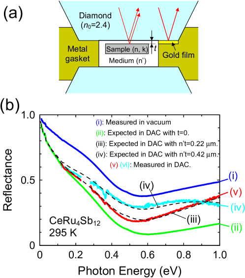
In our experimental condition, as shown in Fig. 8(a), a very thin layer of pressure medium was present between the diamond face and the sample surface. This occurred since the surface of the sample was not completely flat while the diamond surface was almost perfectly flat.[41] With such a layer, as shown by red arrows in Fig. 8(a), multiple reflections of light and their interference are expected. In fact, the visible image of a sample loaded into DAC with pressure medium often showed interference fringes (Newton’s rings). This did not seem to affect the measured in the far IR range, as demonstrated by the good agreement between the spectra in Fig. 2(b) and 2(c). In the mid-IR and near-IR ranges where the wavelength was shorter, however, the “expected” , calculated from the measured , did show noticeable difference from the measured , as shown in Fig. 8(b). This shows that the thickness of the medium layer was not negligible compared with the wavelength of light in the mid-IR range. Note that the gold film used as the reference of reflectance did not have such a layer, since it was directly pressed onto the diamond by the gasket, as sketched in Fig. 8(a).
The reflectance under this situation has been theoretically analyzed in detail,[42] and may be expressed, omitting the dependence, as[42]
| (4) |
where
| (5) |
Here, =2.4 is the refractive index of diamond, and are the refractive index and layer thickness of the medium, respectively, is the complex refractive index of the sample, and is the wavelength of light in vacuum. For simplicity, we assume that is a real constant (no absorption and dispersion in the medium), and that the layer thickness is constant, although in reality it may vary over the sample area. Then using and of the sample obtained with the KK analysis of , we calculated with various values of . In Fig. 9, spectra calculated with =0.22 m (iii) and 0.42 m (iv) are shown, which agree well with the measured spectra (v) and (vi), respectively. The magnitude of the obtained is quite reasonable since the visible image of the sample under microscope exhibited no or only one interference fringe when these spectra were measured. This means that 2 should be smaller than or of the same order with the visible wavelength, which is consistent with the obtained values. Note also that both the measured and calculated spectra indicate that the interference effect becomes small below about 0.2 eV.
For each high pressure run, was measured in DAC before applying high pressure, and the obtained value of was used to analyze the subsequently obtained high pressure data. In reality, may also change with pressure, but it was difficult to correctly measure or estimate it. Therefore we assumed the initial value of for the analysis of high pressure data.
6.3 Actual fitting model and examples of fitted spectra
Once the value of was determined, was calculated with a set of parameters, taking into account =2.4 through Eq. (1) and the interference effect through Eq. (4). Then the parameters were adjusted to minimize the deviation of the calculated from the measured one. The fitting was done with “RefFIT”, a dedicated software for spectral fittings developed by Alexey Kuzmenko.[43] Figure 9 shows examples of actual fitting for (4 GPa, 40 K) and (8 GPa, 40 K) data.
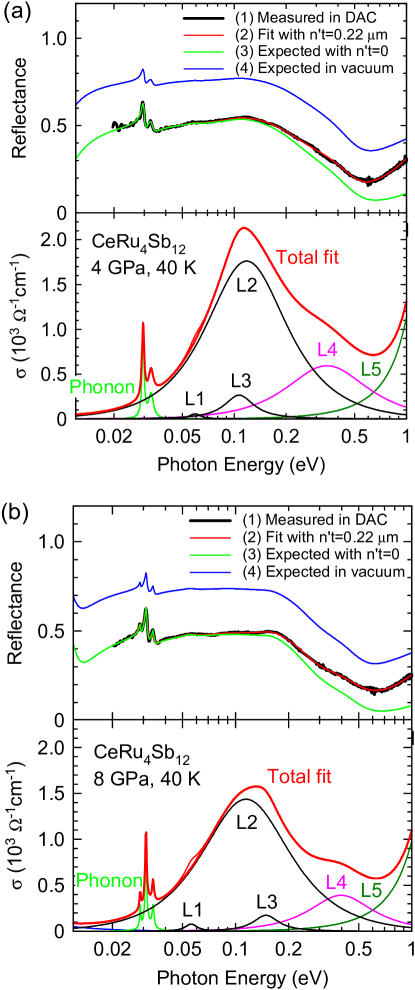
Note that the overall spectral shape of is basically reproduced by one Drude and three Lorentz (L2, L4 and L5) oscillators. Two additional Lorentz oscillators (L1 and L3) were used to cover a small hump of near 60 meV and a shoulder of near 0.1 eV (0.17 eV) at 4 GPa (8 GPa), respectively. The hump at 60 meV is an instrumental artifact,[44] and therefore the and spectra shown in Figs. 4 and 6 were calculated without L1. The shoulder became stronger at low , and therefore the L3 oscillator was necessary for a satisfactory fit. The obtained fitting parameters are listed in Table I. For the Drude component, and were varied to reproduce , and then , namely the dc conductivity given by these parameters, was calculated and compared with the experimentally measured .[13, 14] These values are also listed in Table I. Note that is higher than for most of the data, by a factor of up to 2.1. This is not surprising since a similar result is already seen in the data at 295 K and 0 GPa, where the measured =2600 cm-1 (Ref. 13) is more than twice smaller than that given by the Hagen-Rubens extrapolation (Fig. 1). Similar result was also observed previously.[16] The reason for this is unclear, but there seems to be some scattering mechanism that affects stronger than the high frequency one.
![[Uncaptioned image]](/html/1103.0811/assets/x10.png)
6.4 Uncertainty in the magnitude of obtained conductivity
Compared with the case of KK analysis on a reflectance measured in vacuum, there are many factors that increase the uncertainty in obtained with the above procedures. The largest source of uncertainty is the arbitrariness among the parameters in the DL fitting of performed in a limited energy range (below 1.1 eV). The overall uncertainty in the magnitude of resulting for the high pressure case is estimated to be 10 %. This is indeed much larger than that in the KK-derived in vacuum. However, since we are not making any discussion based on the absolute magnitude of , such as spectral weight transfer or the optical sum rule, the uncertainty should not affect our conclusions.
References
- [1] See, for example, the papers in the Proceedings of the International Conference on High Pressure Science and Technology (Tokyo, 2009), J. Phys. Conf. Ser. 215 (2010).
- [2] See, for example, H. Kotegawa, H. Sugawara and H. Tou, J. Phys. Soc. Jpn 78 (2009) 013709.
- [3] M. Matsunami, H. Okamura, A. Ochiai, and T. Nanba, Phys. Rev. Lett. 103 (2009) 237202.
- [4] See, for example, J. L. Sarrao and J. Thompson, J. Phys. Soc. Jpn. 76 (2007) 051013.
- [5] See, for example, Proceedings of the International Conference on New Quantum Phenomena in Skutterudite and Related Systems, J. Phys. Soc. Jpn. 77 (2008) Suppl. A.
- [6] C. Sekine, N. Hoshi, K. Takeda, T. Yoshida, I. Shirotani, K. Matsuhira, M. Wakeshima, and Y. Hinatsu: J. Magn. Magn. Mater. 310 (2007) 260.
- [7] C. Sekine, R. Abe, K. Takeda, K. Matsuhira and M. Wakeshima: Physica B 403 (2008) 856.
- [8] H. Sato, Y. Abe, H. Okada, T. D. Matsuda, K. Abe, H. Sugawara, and Y. Aoki: Phys. Rev. B 62 (2000) 15125.
- [9] I. Shirotani, T. Uchiumi, C. Sekine, M. Hori, S. Kimura, and N. Hayama: J. Solid State Chem. 142 (1999) 146.
- [10] C. Sekine, K. Akita, N. Yanase, I. Shirotani, I. Inagawa, and C. Lee: Jpn. J. Appl. Phys. 40 (2001) 3326.
- [11] N. Takeda and Y. Ishikawa: J. Phys. Soc. Jpn. 69 (2000) 868.
- [12] E. D. Bauer, A. Slebarski, R. P. Dickey, E. J. Freeman, C. Sirvent, V. S. Zapf, N. R. Dilley, and M. B. Maple: J. Phys.: Condens. Matter 13 (2001) 5183.
- [13] M. Kobayashi, S. R. Saha, H. Sugawara, T. Namiki, Y. Aoki, and H. Sato: J. Magn. Magn. Mater. 329-333 (2003) 605.
- [14] N. Kurita, M. Hedo, Y. Uwatoko, M. Kobayashi, H. Sugawara, H. Sato, and N. Mori: Physica B 272-276 Suppl. 1 (2004) E81.
- [15] N. Kurita, H. Hedo, M. Koeda, M. Kobayashi, H. Sato, H. Sugawara, and Y. Uwatoko: Phys. Rev. B 79 (2009) 014441.
- [16] S. V. Dordevic, D. N. Basov, N. R. Dilley, E. D. Bauer, and M. B. Maple: Phys. Rev. Lett. 86 (2001) 684.
- [17] M. Matsunami, H. Okamura, T. Nanba, H. Sugawara, and H. Sato: J. Magn. Magn. Mater. 272-276 (2004) e41.
- [18] S. V. Dordevic, K. S. D. Beach, N. Takeda, Y. J. Wang, M. B. Maple, and D. N. Basov: Phys. Rev. Lett. 96 (2006) 017403.
- [19] M. Matsunami, H. Okamura, T. Nanba, H. Sugawara, and H. Sato: J. Phys. Soc. Jpn. 72, 2722 (2003).
- [20] H. Okamura, T. Michizawa, T. Nanba and T. Ebihara: J. Phys. Soc. Jpn. 73 (2004) 2045.
- [21] G. Burns: Solid State Physics, Chapter 13 (Adademic Press).
- [22] M. Dressel and G. Gruner: Electrodynamics in Solids (Cambridge Press).
- [23] H. Okamura, M. Matsunami, R. Kitamura, S. Ishida, A. Ochiai, and T. Nanba: J. Phys.: Conf. Ser. 215 (2010) 012051.
- [24] N. Tateiwa and Y. Haga: Rev. Sci. Instr. 80 (2009) 123901.
- [25] T. Moriwaki and Y. Ikemoto: Infrared Phys. Tech. 51 (2008) 400.
- [26] B. C. Webb, A. J. Sievers, and T. Mihalisin: Phys. Rev. Lett. 57 (1986) 1951.
- [27] J. N. Hancock, T. McKnew, Z. Schlesinger, J. L. Sarrao, and Z. Fisk: Phys. Rev. Lett. 92 (2004) 186405.
- [28] H. Okamura, T. Watanabe, M. Matsunami, T. Nishihara, N. Tsujii, T. Ebihara, H. Sugawara, H. Sato, Y. Onuki, Y. Isikawa, T. Takabatake, and T. Nanba: J. Phys. Soc. Jpn. 76 (2007) 023703.
- [29] S. Kimura, T. Iizuka, and Y.-S. Kwon: J. Phys. Soc. Jpn. 78 (2009) 013710.
- [30] S. Kimura, Y. Muro, and T. Takabatake: J. Phys. Soc. Jpn. 80 (2011) 033702.
- [31] H. Okamura, T. Michizawa, T. Nanba, S. Kimura, F. Iga, and T. Takabatake: J. Phys. Soc. Jpn. 74 (2005) 1954.
- [32] P. Y. Yu and M. Cardona: Fundamentals of Semiconductors (Springer, Berlin, 2001) 3rd ed., Chapter 6.2.
- [33] G. G. MacFarlane, T. P. McLean, J. E. Quarrington and V. Roberts: Phys. Rev. 108 (1957) 1377.
- [34] B. Bucher, Z. Schlesinger, P. C. Canfield, and Z. Fisk: Phys. Rev. Lett. 72 (1994) 522.
- [35] K. Abe, H. Sato, T. D. Matsuda, T. Namiki, H. Sugawara, and Y. Aoki: J. Phys. Condens. Mat. 14 (2002) 11757.
- [36] H. Sugawara, K. Abe, T. D. Matsuda, Y. Aoki, H. Sato, R. Settai, and Y. Onuki: Physica B 312-313 (2002) 264.
- [37] H. Harima and K. Takagahara: J. Phys.: Condens. Matter 15 (2003) S2081.
- [38] M. Matsunami, H. Okamura, K. Senoo, S. Nagano, C. Sekine, I. Shirotani, H. Sugawara, H. Sato, T. Nanba: J. Phys. Soc. Jpn. 77 (2008) Suppl. A, pp. 315.
- [39] T. Mutou and T. Saso: J. Phys. Soc. Jpn. 73 (2004) 2900.
- [40] T. Saso, J. Phys. Soc. Jpn. 75 (2006) 043705.
- [41] It is possible to avoid such a layer of medium between the diamond and sample by using a solid pressure medium such as KBr and NaCl. At pressures below 10 GPa, however, liquid pressure medium such as glycerin can provide much more hydrostatic pressure than KBr.[24] In view of the importance of having a more hydrostatic pressure for studying electronic structures of strongly correlated materials, we chose glycerin over solid medium despite the complications in data analysis discussed here.
- [42] O. S. Heavens, Optical Properties of Thin Solid Films (Dover, New York, 1991).
- [43] A. B. Kuzmenko: RefFIT, available at http://optics.unige.ch/alexey/reffit.html.
- [44] This hump of results from a small hump of at 60 meV seen in Figs. 3(b) and 3(c) at a few temperatures. To fit this hump, an additional oscillator L1 was used as shown in Fig. 9 (Appendix). The hump in is also present in the low pressure (0.2 GPa) DAC data of Fig. 2(c), but not in the zero pressure data of Figs 1, 2(a) and 2(b). We conclude that this hump is an instrumental artifact created by the spectroscopy apparatus used for the high pressure experiment, presumably due to a structure in the spectral response of the beam splitter in the IR interferometer.