Band alignment at metal/ferroelectric interfaces: insights and artifacts from first principles
Abstract
Based on recent advances in first-principles theory, we develop a general model of the band offset at metal/ferroelectric interfaces. We show that, depending on the polarization of the film, a pathological regime might occur where the metallic carriers populate the energy bands of the insulator, making it metallic. As the most common approximations of density functional theory are affected by a systematic underestimation of the fundamental band gap of insulators, this scenario is likely to be an artifact of the simulation. We provide a number of rigorous criteria, together with extensive practical examples, to systematically identify this problematic situation in the calculated electronic and structural properties of ferroelectric systems. We discuss our findings in the context of earlier literature studies, where the issues described in this work have often been overlooked. We also discuss formal analogies to the physics of polarity compensation at LaAlO3/SrTiO3 interfaces, and suggest promising avenues for future research.
pacs:
71.15.-m, 73.61.-r, 77.55.-g, 77.80-eI Introduction
Advances in oxide thin film growth techniques over the last ten years have led to the fabrication of many novel oxide-based metal-insulator heterostructures with a dizzying range of functionalities. Not only are the current technological limits of information storage density and speed being pushed forward by the use of, e.g., nanoscale ferroelectric memories, Scott and de Araujo (1989); Auciello et al. (1998); Scott (2000); Dawber et al. (2005); Scott (2006, 2007) but entirely new concepts in device applications are also emerging, in which the electrical and the magnetic degrees of freedom are both present within the same active element and strongly coupled. Fiebig (2005); Eerenstein et al. (2006) Examples of this trend include thin-film capacitors, Dawber et al. (2005) strongly correlated field-effect devices, Ahn et al. (2003) and magnetic/ferroelectric tunnel junctions.Tsymbal and Kohlstedt (2006); Maksymovych et al. (2009); García et al. (2009, 2010)
Density functional theory (DFT) methods, either within the local density (LDA) or generalized gradient (GGA) approximation, have been an invaluable tool in achieving a fundamental understanding of this class of systems,Dawber et al. (2005); Ghosez and Junquera (2006); Junquera and Ghosez (2008) particularly with recent developments which allow the application of finite electric fields to periodic solids or layered heterostructures. Souza et al. (2002); Umari and Pasquarello (2002); Souza et al. (2004); Stengel and Spaldin (2007); Stengel et al. (2009a) However, since this domain of research is relatively new, it is important to identify, in addition to the virtues, also the limitations of DFT that are specific to metal/ferroelectric interfaces, and that when overlooked might lead to erroneous physical conclusions.
For most practical applications, a capacitor must be insulating to DC current; transmission of electrons via non-zero conductivity and/or direct tunneling (leakage) is generally an undesirable source of heating and power consumption. At the quantum mechanical level, the insulating properties of a capacitor are guaranteed by the presence of a dielectric film with a finite band gap at the Fermi level, where propagation of the metallic conduction electrons is forbidden. In the language of semiconductor physics, we can alternatively say that both Schottky barrier heights (SBH), respectively and for electrons and holes, need to be positive for the device to behave as a capacitor. (By convention we assume that, if the Fermi level of the metal lies in the gap of the insulator, both and are positive.)
If, on the contrary, either or is negative, injection of holes or electrons into the dielectric becomes energetically favorable and the device behaves instead as an Ohmic contact. Most importantly, at such a junction there is necessarily (at thermodynamic equilibrium) a spill-out of charge from the metal to the insulator, as the system re-equilibrates the chemical potential of the free carriers on either side. Such intrinsic space charge induces metallicity (by intrinsic doping) in the dielectric film, and overall profoundly alters the electronic and structural properties of the interface.
While in principle the charge spillage might be a real physical feature of a given system, there are several arguments that advise caution in the interpretation of DFT calculations where this effect is found. The use of an approximate functional to model the exchange and correlation energy, such as LDA or GGA, generally produces severe and systematic errors in the values of and , which can be generally traced back to the well-known band-gap problem. Perdew and Levy (1983); Sham and Schlüter (1983) This implies that finding a negative value of either or is unlikely to be a robust result of an LDA or GGA calculation. Furthermore, the total amount of spilled-out charge depends on the DFT values of and (the more negative the SBH, the larger the number of states of the insulator that cross the Fermi level). This means that, in such a pathological regime, the error in or will directly propagate to the charge density, and potentially affect a number of fundamental ground-state properties of the interface. In order to avoid undesirable artifacts in the DFT results, it is therefore crucial to clearly identify whether this scenario applies to a given interface calculation.
Such an analysis is not entirely straightforward, as physics governing the band alignment in a ferroelectric capacitor significantly departs from the well-established concepts of semiconductor physics. First, the imperfect screening at the electrode interface produces a potential drop Stengel and Spaldin (2006); Junquera and Ghosez (2008) that is roughly linear in the polarization ,Junquera and Ghosez (2003) and modifies the lineup between the bands of the insulator and the Fermi level of the metal. Stengel et al. (2009a) This phenomenon, central to the physics of ferroelectric capacitors, has important implications for the stability of a monodomain polar state,Junquera and Ghosez (2008) and for devices based on the tunneling electroresistance effect. Zhuravlev et al. (2005) Second, the residual “depolarizing” electric field produces a linearly increasing electrostatic potential in the film. This prevents a precise determination of the band lineup, Stengel et al. (2009a) as a proper (and physically meaningful) definition of the latter requires a macroscopically constant reference energy in the insulating region. Third, the marked covalent character of bonding in perovskites produces non-trivial changes in the band structure of the insulator, depending on the magnitude of the polar distortion. This further complicates the extraction of an accurate band lineup by means of standard first-principles procedures, as the bulk reference calculation needs to accurately match the electrical, in addition to the mechanical, boundary conditions of the film. Finally, and most importantly, one must keep in mind that all these new physical ingredients may coexist with the more traditional features that are typical of metal/semiconductor interfaces, e.g. the phenomenon of metal-induced gap states (MIGS).Heine (1965) To guide future works in this field, and to build a firm theoretical basis for the interpretation of the experiments, it is becoming increasingly urgent to rationalize all these many competing effects into a coherent picture, where the limitations of the current simulation methods can be clearly drawn.
Here we develop a general and intuitive model of the band offset at a ferroelectric/metal interface, and its dependence on the polarization. We identify two qualitatively distinct regimes, corresponding to (i) that of a normal Schottky alignment and (ii) that of a pathological Ohmic junction. We demonstrate the artifacts typically associated with (ii) by performing extensive calculations of technologically relevant ferroelectric/metal interfaces. We discuss the relevant literature works, pointing out those where our results suggest a revision of the currently accepted interpretation. We further identify a direct relationship between the pathological Ohmic regime and the physics of “electronic reconstruction” Okamoto and Millis (2004) at polar oxide interfaces such as LaAlO3/SrTiO3, and trace a viable route towards a unified description of these two phenomena. Finally, we discuss a number of viable methodological perspectives to overcome the limitations of DFT illustrated in this work.
The paper is organized as follows: In Sec. II we develop our theoretical model of the band offset at a ferroelectric/metal interface, illustrating the main consequences of a “pathological” band alignment. In Sec. III we present a self-contained overview of the theoretical methods we use to detect such features in a first-principles calculation. In Sec. IV we present the results of our simulations for paraelectric capacitors, by comparing non-pathological (PbTiO3/SrRuO3 and BaTiO3/SrRuO3) and pathological cases (KNbO3/SrRuO3 and BaTiO3/Pt). In Sec. V we demonstrate that the two cases which we find to be non-pathological in the paraelectric configuration indeed become pathological when the polarized ferroelectric state is fully relaxed. In Sec. VI we discuss the implications of this work with respect to the existing literature on the subject. Finally, in Sec. VII we present our conclusions and outlook for future research.
II General theory of the band offset
II.1 Metal/semiconductor interfaces
The Schottky barrier, a rectifying barrier for electrical conduction across a metal/semiconductor junction, is of vital importance for the operation of any modern electronic device. For the case of an -type semiconductor, the Schottky barrier height is the energy difference between the conduction band minimum and the Fermi level across the interface, and we indicate it as . The nature of the microscopic mechanisms governing the magnitude of has troubled scientists for several decades. In spite of the ongoing debates, it seems to be widely accepted now that, while bulk material properties certainly play a substantial role, is best understood as a genuine interface property. This is in agreement with the intuitive picture one gets from quantum mechanics: the charge rearrangement due to chemical bonding at the interface produces an interface dipole, and this will uniquely determine the offset between the energy bands of the insulator and the Fermi level of the metal.

To be more specific, it is useful to consider the electrostatic Hartree potential at the interface between two semi-infinite solids,
| (1) |
where is the total charge density (including electrons and nuclei). is a rapidly varying function of the position, reflecting the underlying atomic structure. In order to filter out the large oscillations and preserve only those features that are relevant on a macroscopic scale, it is convenient to apply an averaging procedure. Baldereschi et al. (1988); Colombo et al. (1991) This consists of (i) performing a global average of over planes parallel to the interface, and (ii) convoluting the resulting one-dimensional function with a Fourier filter to suppress the high spatial frequency components. (See Ref. Junquera et al., 2007 for a detailed description of the method, and Ref. Franciosi and de Walle, 1996 for an extensive review of its applications to SBH calculations.) After this “nanosmoothing” Junquera et al. (2007) procedure, the doubly-averaged reduces to a step function, from which we can extract the electrostatic lineup term, Baldereschi et al. (1988); Colombo et al. (1991)
| (2) |
which includes all the physics of the interface dipole formation. [ and are the asymptotic values of far from the interface.] To determine the band offsets from it is then necessary to know how the bulk energy bands of the insulator and the Fermi level of the metal are related to their respective average electrostatic potential. In full generality, one can write
| (3a) | ||||
| (3b) | ||||
, and are usually referred to as the band structure term, Baldereschi et al. (1988); Colombo et al. (1991) and are bulk properties of the two materials. They are defined as the energy positions of the valence () and conduction () band edges of the insulator, and the Fermi level of the metal (), all referred to the average in the respective bulk (see Fig. 1).
In Sec. III we provide further details of the standard computational procedures used to calculate these quantities in practice. In the following Section we discuss how the above theory needs to be revised and extended in the case of metal/ferroelectric interfaces.
II.2 Metal/ferroelectric interfaces
Ferroelectric materials entail a new degree of freedom, the macroscopic polarization , which is absent in the semiconductor case. It is natural then to expect that the above picture of the band offset at metal/insulator interfaces may need to be extended to take this new variable into account. In the following, we discuss how affects both the lineup and the band-structure terms in Eqs. (3a) and (3b).
II.2.1 Lineup term
We represent a simple ferroelectric material as a non-linear dielectric, which in bulk is characterized by an internal energy per unit cell of the form
| (4) |
Here is the electric displacement field, is an arbitrary reference energy, is negative and the highest expansion coefficient positive. (As we are concerned with the essentially one-dimensional case of a parallel-plate capacitor, we only consider the component of the vector that is normal to the interface plane, indicated as henceforth.) The coefficients implicitly contain all the complexity of the microscopic physics, and can be calculated from first principles using the methods of Ref. Stengel et al., 2009b. It follows from elementary electrostatics Stengel et al. (2009b) that the internal electric field, , is the derivative of ,
| (5) |
where is the cell volume.
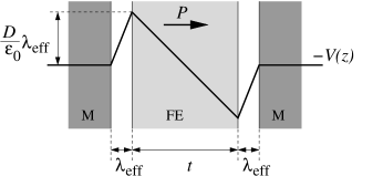
The electrostatics of a parallel-plate capacitor configuration can be well described Stengel and Spaldin (2006); Stengel et al. (2009c); Junquera and Ghosez (2003) within the imperfect screening model, as sketched in Fig. 2. The -layer thick ferroelectric film can be thought of as separated from the ideal metal electrode by a thin layer of vacuum, of thickness . is an “effective screening length” that takes into account all the microscopic details of the interface dipole response to the polarization, Junquera and Ghosez (2003) including electronic and chemical bonding effects. Stengel et al. (2009c) At the interface between the ferroelectric and the vacuum layer must be preserved. Therefore, an homogeneous electric field appears inside the vacuum layer, of magnitude . Recalling that the energy density of a static electric field in vacuum is , the energy of the -layer thick ferroelectric film can then be written as
| (6) |
where is the surface cell area. [Note that two symmetric electrodes of equal are considered in Eq. (6).] The second important consequence of a non-zero is that the lineup term, Eq. (2), now linearly depends on the external parameter , due to the additional potential drop at the interface, that can be computed as the product of the electric field within the vacuum layer times its width,
| (7) |
[It is worth noting that, whenever , at the microscopic level contains an intrinsic arbitrariness; furthermore, in such a case it is no longer justified to think in terms of an “isolated” interface between two semi-infinite solids. Techniques to deal with these issues in practical calculations are described in Ref. Stengel et al., 2009a.]
| (C/m2) | (Å) | (V) | |
|---|---|---|---|
| BaTiO3 | 0.39 | 0.20 | 1.8 |
| PbTiO3 | 0.75 | 0.15 | 2.6 |
To give a more quantitative flavor of the impact of this -dependence in real systems, we can use the values of reported in the literature for PbTiO3/SrRuO3 and BaTiO3/SrRuO3 capacitors. Upon polarization reversal, the interface lineup term will undergo a variation corresponding to
| (8) |
where is the spontaneous polarization of the ferroelectric material (in the spontaneous configuration the internal electric field within the ferroelectric, , vanishes and equals the spontaneous polarization.) The values reported in Table 1 indicate that this effect can be rather large, of the order of 1-2 eV, even for ideal defect-free interfaces.
II.2.2 Band-structure term
The polar displacements in the ferroelectric film modify not only the lineup term, but also the bulk band-structure term. This is most easily understood by recalling the role played by covalent bonding in the ferroelectric instability of perovskite titanates. Hybridization effects between the cation states and the oxygen states are intimately linked to the off-centering of the Ti sublattice. This implies that the polar distortions can significantly modify both the conduction and valence band structure. For example, in both BaTiO3 and PbTiO3 the fundamentamental gap increases when going from the centrosymmetric cubic structure to the polar tetragonal phase. Using the arguments of Ref. Stengel et al., 2009a, we can think of a continuous dependence of both and , respectively in Eq. (3a) and Eq. (3b), on the electric displacement . The Fermi level , of course, remains fixed as the electric displacement does not affect the bulk of the metallic electrode. In summary, the general expression for the -type SBH at a metal/ferroelectric interface (an analogous expression follows for the -type one) is
| (9) |
where at the lowest order is quadratic in (the linear order is forbidden by symmetry), and in most cases of interest can be approximated by a linear function as in Eq. (7). In the following, we shall elaborate on this expression and identify a new, qualitatively different regime, with important implications for the physics of the interface.
II.3 Ferroelectric capacitors in a pathological regime
Equation (9) implies that might become negative for some values of . From the point of view of first-principles calculations, already by looking at the values of Table 1 we can be reasonably sure that this will happen at the PbTiO3/SrRuO3 interface: 2.6 eV is already larger than the LDA gap of PbTiO3 in the ferroelectric phase (2.0 eV). This possibility has been almost systematically overlooked in the literature. As this is a central point of this work, we shall illustrate in detail the consequences of such a regime, and explain why we regard it as “pathological”. We discuss in the following two possible occurrences of this scenario: (i) is negative already in the paraelectric configuration at and (ii) is positive at but becomes negative at some value of .
II.3.1 The centrosymmetric case
We start with a capacitor in the reference paraelectric structure with two symmetric electrodes, and we hypothesize that, for whatever physical reason, the interface dipole that forms between the metal and the film leads to a negative . (Similar arguments apply to the case, not explicitly discussed here, of a negative .) As the quantum states of the conduction band of the film lie at lower energy than the Fermi level of the metal, the former will be filled up to , leading to a nonzero free charge density, , in the film. Neglecting quantum confinement effects, we can use the Thomas-Fermi model and treat the free charge distribution as macroscopically uniform. Within this approximation, is exactly given in terms of and the electronic density of states of the bulk insulator, , in a vicinity of the conduction band bottom, ,
| (10) |
This additional charge density, superimposed on an otherwise charge-neutral insulating film, will produce a strong electrostatic perturbation in the system. For example, if such a charge rearrangement occurred in vacuum, the Poisson equation
| (11) |
would imply a parabolic potential of the form
| (12) |
(We assume that corresponds to the center of the ferroelectric film.) Throughout this work, we shall assume that the interface is oriented along the axis, and each material is periodic in the plane parallel to the interface, referred to as the plane. As typical ferroelectric materials are exceptionally good dielectrics, in a first approximation we can assume that will be perfectly screened by the polar displacements of the lattice. However, this does not mean that electrostatics has no consequences – quite the contrary. Macroscopic Maxwell equations in materials indeed dictate that
| (13) |
Hence, if we assume perfect bulk screening, we have , and, after integrating Eq. (13), . So, since the sign of the electronic charge and are negative within our convention, we have a non-uniform and linearly decreasing polarization in the ferroelectric film [see Fig. 3(d)]. This means that, at the film boundaries (, where is the thickness), the local electric displacement has now opposite values, proportional to the total amount of free charge that was transferred,
| (14) |
Of course, the band offset at the interface depends on the local value of in the film region adjacent to the interface, so will be consequently shifted in energy according to Eq. (9). We can expect that for small values the (quadratic) polarization effects on the band structure will be less important than the (linear) dependence of the lineup term on . (Note that the presence of additional charge in the conduction band might also alter the bandstructure term, e.g. through on-site Coulomb repulsions or other exchange and correlation effects; in the limit of weak correlations we expect these to be even smaller and essentially irrelevant for this discussion.) Therefore, we approximate Eq. (9) with Eq. (7), and write
| (15) |
[The minus sign comes from the fact that at the interface, which is the one for which Eq. (7) is valid within our conventions, is negative.] In turn, the new will modify through Eq. (10). For some value of , Eq. (10) and Eq. (15) will be mutually self-consistent and the system will reach electrostatic equilibrium. This can be expressed through an integral equation where we have eliminated ,
| (16) |
To qualitatively appreciate the physical implications of this expression, we can explicitly solve it by using a constant . (Note that this assumption is not completely unrealistic as the bands forming the bottom of the conduction band in many ferroelectric perovskites have a marked 2D character; in other words, the in-plane effective mass is much smaller than the out-of-plane one, . Within the approximation , the constant density of states of the six-fold degenerate, free-electron-like 2D band is uniquely determined by .) This leads to
| (17) |
and with a few rearrangements to
| (18) |
where is a constant, and is the density of states per unit energy and volume of the bulk. In spite of the drastic simplifications, Eq. (18) already contains most of the relevant ingredients for our analysis. A few notable ones are missing – we shall come back to those in Sections II.3.2 and II.3.3. Before going into more detailed considerations, however, it is important to spell out the direct implications of Eq. (18), which we shall be concerned with in the following.
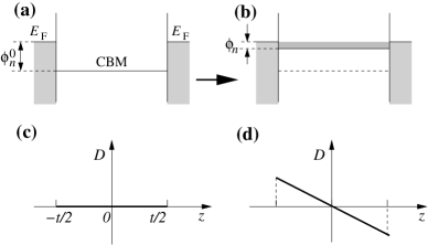
First, note that all quantities appearing at the denominator at the right-hand side of Eq. (18) are positive. This means that will be negative, and will satisfy . The lower limit corresponds to the perfect interface screening case, . The upper limit corresponds to no screening, . The situation is schematically represented in Fig. 3(a) and Fig. 3(b). Given a negative [Fig. 3(a)], the charge redistribution will induce an upward energy shift of the conduction band minimum (CBM), bringing closer to the Fermi level [Fig. 3(b)]. Second, in the limit of (infinite thickness) will tend to zero from below as . This means that the self-consistent band offset is not determined by the local physical properties of the junction, i.e. it is no longer an interface property – the spilled-out charge will redistribute over the whole film thickness as is varied. Third, the density of states of the conduction band, represented in Eq. (18) by the parameter , will also affect the value of : the larger , the strongest the reduction in upon charge spill-out and electrostatic re-equilibration. (To avoid confusion, note that in the above paragraphs, we used the word “screening” in two different contexts. By “perfect bulk screening” we mean . By “perfect interface screening” we mean .)
We can attempt a semiquantitative assessment of Eq. (18) in a representative capacitor of thickness Å (comparable to those that are typically simulated within DFT). In atomic units, we use (of the order of the values reported in Table 1), , and (appropriate for the conduction band of SrTiO3, a prototypical perovskite material, with a calculated and a.u.). We obtain
| (19) |
This implies that the effect is quite strong – even if is a rather large negative value (e.g. of the order of -1 eV), in most practical cases the conduction charge redistribution will reduce it to a value that lies just below the Fermi level. Most importantly, this implies that, when , the physical parameters, and , governing the band offset at the interface are neither accessible in a simulation, nor are they directly measurable in an experiment – only might be. Note, however, that the “self-consistent” value is generally not a well-defined physical quantity – this is only true within the many approximations used in the above derivations. In particular, we have neglected band-bending effects: in general the electrostatic potential will be non-uniform in the film (see Sec. II.3.3) and will be a function of the distance from the interface. But even if we put this caveat aside for a moment, the reader should keep in mind that is determined here by space-charge effects through several independent contributions. Furthermore, the film is no longer insulating but becomes a metal. This is a substantial, qualitative departure from the physical concepts that were developed in the context of semiconductor/metal interfaces, and that led to the consensus understanding of as a genuine interface property.
Given this situation, one needs to revisit the very foundations of the methodological ab-initio approaches that have been used with great success in the past to compute Schottky barrier heights. This success has critically relied on a key observation: the interface dipole, that one identifies with the lineup term Eq. (2), is a ground-state property, i.e. is not directly affected by the well-known limitations of the Kohn-Sham eigenvalue spectrum. This is excellent news: one can efficiently (and accurately) calculate within DFT, and combine it with a band-structure term ( or ) calculated at a higher level of theory (e.g. GW); within this formally sound procedure, theoretical calculations have shown remarkable agreement with the experimental observations in the past.
In the spill-out regime (i.e. ) described in this Section the above key observation no longer holds – the erroneous DFT value of plays a direct and dominant role in the interface dipole formation, as is apparent from Eq. (18). Furthermore, as is systematically underestimated within LDA or GGA, there is the concrete possibility that the spill-out regime itself () might be an artifact of the band-gap problem. Thus, the ground-state properties of the system found in a simulation might be qualitatively wrong due to this issue, in loose analogy to, e.g., the erroneous LDA prediction of metallicity in many transition metal compounds. It goes without saying that the results of a simulation where significant spill-out of charge is found because of the mechanism described in this Section should be regarded with great suspicion.
II.3.2 The broken-symmetry case
Even if the band aligmnent is Schottky-like in the reference paraelectric structure of the capacitor, Eq. (9) entails the possibility that it might become pathological in the ferroelectric regime (i.e. when the polar instability is allowed to fully relax). Unfortunately, for this case many of the simplifying assumptions used above are no longer valid, and for a detailed description one would need to take into account the more refined physical ingredients discussed in Sec. II.3.3. At the qualitative level, however, we can already draw some important conclusions, as we shall briefly illustrate in the following.
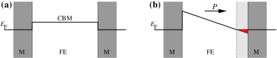
Eq. (9) predicts that, if is positive and the capacitor is compositionally symmetric [as in Fig. 4(a)], at finite at most one of the two opposite interfaces will have a negative . This implies that only part of the ferroelectric film, i.e. the region adjacent to this “pathological” interface, will become metallic, while the rest of the film will stay insulating [Fig. 4(b)]. (To understand this point, note that in contrast with the previous case one has now a finite “depolarizing” electric field in the insulating part of the capacitor. This wedge-like potential will keep the conduction electrons electrostatically confined to the pathological side.) In the insulating region, the polarization will be macroscopically constant, as in a well-behaved capacitor [recall Eq. (13)]. According to the same Eq. (13), [and hence ] will be non-homogeneous, with a negative slope, in the metallic region.
In this context it is worth pointing out an important physical consequence of such a peculiar electronic ground state. This concerns the response of the capacitor to an applied bias potential. In well-behaved cases, the polarization of the capacitor will respond uniformly to a bias, i.e. all the perovskite cells up to the electrode interface will undergo roughly the same polar distortion. In the present “ferroelectric-pathological” regime, part of the ferroelectric film has become metallic, i.e. the metal/insulator interface has moved to a place that lies somewhere in the film. This means that, if one tries to switch the device with a potential, the electric field won’t affect the dipoles that lie closest to the pathological interface – they will be screened by the spilled-out free charge. A consequence is that the dipoles near a pathological interface will appear as if they were pinned to a fixed distortion, that is almost insensitive to the electrical boundary conditions. This pinning phenomenon has been studied in earlier theoretical works, and was ascribed to chemical bonding effects. In Sec. V we shall substantiate with practical examples that “dipole pinning” is instead a direct consequence of the problematic band-alignment regime described here. In Sec. VI we shall come back to this point and put it in the context of the relevant literature.
II.3.3 Towards a quantum model
In order to draw a closer connection between the semiclassical arguments of the previous sections and the quantum-mechanical results that we present in Sections IV and V, we briefly discuss here how to improve our physical understanding of the charge spill-out process by lifting some of the simplifying approximations used so far. As a detailed treatment goes beyond the scope of the present work, we shall limit ourselves to qualitative considerations.
The most drastic approximation of our model appears to be the assumption of perfect dielectric screening within the ferroelectric material, where the spill-out charge is perfectly compensated by the polar displacements of the lattice. This implies that the electric field in the film vanishes, and the excess conduction charge can spread itself spatially at essentially no cost. In this scenario, the macroscopically uniform distribution of postulated in Sec. II.3.1 appears very reasonable. In reality, the internal field in the bulk ferroelectric material does not vanish, but is a non-linear function of , that can be written by combining Eq. (4) and Eq. (5),
| (20) |
Of course, solving for the self-consistent in a non-linear medium would require a numerical treatment. Still, we can gain some insight about qualitative trends by starting, for example, from the linearly decreasing found in the case of Sec. II.3.1. Using Eq. (20) we can write . The electrostatic potential is then given by integrating . This essentially leads to , where is the internal electrostatic energy of Eq. (4), and is a (positive) constant with the dimension of a charge. This means that the spatial variation in reflects the energy landscape of the bulk material: will be a double-well potential in a ferroelectric material (), and a single-well potential in a paraelectric material (). Remarkably, the double-well potential accounts for the possibility of free-charge accumulation in the middle of the centrosymmetric film [Fig. 5(a)], which would produce a head-to-head domain wall in the polarization . Conversely, for a paraelectric material one would expect the free charge to be (more or less loosely) bound to the interface, and have a minimum in the middle of the film [Fig. 5(b)]. Of course, these considerations are valid for a centrosymmetric capacitor, and are presented just to give the reader an idea of the physics – in the ferroelectric case, more complex patterns can occur and exploring them all would require an in-depth study that is beyond the scope of this manuscript.
A second important approximation is the neglect of (i) quantum confinement effects beyond the simple Thomas-Fermi filling of the bulk-like density of states and (ii) the band-structure changes due to the polar distortions, which we briefly mentioned in Sec. II.2.2. These will further modify the equilibrium distribution of the free charge, and we expect them to be important to gain a truly microscopic understanding of the system, although not essential for the points of this work. Remarkably, a promising model taking all these ingredients into account (dielectric non-linearity and band-structure effects) was recently proposed in the context of the (at first sight unrelated) LaAlO3/SrTiO3 interface. Stengel (2010) This indicates that the physics of a ferroelectric capacitor in the pathological band-alignment regime described here is essentially analogous to that of the “electronic reconstruction” Okamoto and Millis (2004) in oxide superlattices. Further work to explore these interesting analogies is under way.
II.4 Implications for the analysis of the ab-initio results
The above derivations show that there are two qualitatively dissimilar regimes in the physics of a metal/insulator interface, Ohmic-like and Schottky-like. During the derivation, we have evidenced some distinct physical features that we expect to be intimately associated with the “pathological” Ohmic case. As these are of central importance to help distinguish one scenario from the other, we shall briefly summarize them in the following, mentioning also how each of these “alarm flags” can be detected in a first-principles simulation.
First, even after the electron re-equilibration takes place, the band edges cross the Fermi level of the metal, i.e. the apparent Schottky barrier is negative. Therefore, the analysis of the local electronic structure and of the SBH appears to be the primary tool to identify a pathological case. However, as the “self-consistent” tends to stay very close to the Fermi level, this analysis should be performed with unusual accuracy – techniques to do this will be discussed in Sec. III.1.
Second, the presence of a substantial density of free charge populating the conduction band of the insulator is another important consequence of the pathological regime. In Sec. III.2.1 we illustrate how to rigorously define in a ferroelectric heterostructure.
Finally, a remarkable consequence of charge spill out is the presence of an inhomogeneous polarization in the system. Note that this feature has been ascribed in earlier works to phenomena of completely different physical origin. We shall devote special attention in Sections IV and V to demonstrating the intimate relationship between and spatial variations in .
III Methods
In this Section we spell out the practical techniques that we use to extract the SBH from first-principles calculations, the operational definitions of free charge and bound charge, and the methods we use to control the electrical boundary conditions in supercell calculations. We also summarize the other relevant computational parameters used in Sections IV and V.
III.1 Schottky barrier estimations
First, we briefly review the methods that were used in earlier works to compute Schottky barriers at metal/semiconductor interfaces, pointing out advantages and limitations of each of them. Then, we illustrate potential complications that might arise, with special focus on ferroelectric oxide systems and the issues discussed in Sec. II.
III.1.1 From the local density of states
In order to calculate the band offset at a metal/insulator interface, one needs to identify the location of the band edges deep in the insulating region, with the Fermi level of the metal taken as a reference. To that end, it has become common practicePeressi et al. (1998) to define a spatially-resolved density of states,
| (21) |
where is a normalized function, localized in space around the region of interest. When is an eigenstate of the position operator, the resulting is commonly known as local density of states (LDOS). Conversely, when is an atomic orbital of specified quantum numbers , we call it instead projected density of states (PDOS). The integral is performed over the first Brillouin zone (BZ) of the supercell and the sum runs over all the bands . stands for the eigenvalue of the electronic wave function .
The LDOS defined in Eq. (21), that depends on the position in real space as well as on the energy, gives a very intuitive picture of the band offset: “sufficiently far” away from the interface, the LDOS converges to a bulk-like curve, Peressi et al. (1998) and in principle the location of the band edges (and hence the SBH) can be directly extracted by visual inspection. However, several approximations are used in practice to make the calculation tractable, and these can introduce significant deviations in the SBH computed by means of either the LDOS or PDOS. First, all studies are done on a finite supercell, usually with a symmetric capacitor geometry. This implies that the LDOS of the most dispersive bands will be altered by quantum confinement effects, which might produce a spurious gap opening. Also, the LDOS associated to the evanescent metal-induced gap states (MIGS) might be still important at the center of an insulating film that is not thick enough, thus preventing an accurate identification of the band edge. Second, a discrete -point mesh is used instead of the continuous one implicitly assumed in Eq. (21). Such a -point mesh is generally optimized for efficiency, which means that high-symmetry (HS) points are often excluded. k-p As the edges of the valence and conduction band manifolds are usually located at the HS points,Ban estimating those features from the calculated LDOS might lead to substantial inaccuracies. For materials that display a very dispersive band structure (see e.g. Ref. Delaney et al., 2010) it is not unusual to have deviations of the order of several tenths of an eV. Third, a fictitious electronic temperature (or Fermi surface smearing) is commonly used, in order to alleviate the errors introduced by the -mesh discretization. This implies that the Dirac delta function in Eq. (21) needs to be replaced by a normalized smearing function (e.g. a Gaussian) with finite width. This is a again potential source of inaccuracies, because the apparent edges of the smeared LDOS/PDOS actually might not correspond to the physical band edges but to the (artificial) tail of the smearing function used.
Summarizing the above, we get to the following operational definition of the smeared LDOS,
| (22) |
where the BZ integral has been replaced with a sum over a discrete set of special points with corresponding weights , and the Dirac delta has been replaced with a smearing function . As will become clear shortly (a detailed analysis is provided in Appendix B), it is very important to use in Eq. (22) a function that is minus the analytical derivative of the occupation function used in the actual calculations. The Gaussian smearing (G) and the Fermi-Dirac (FD) smearing are by far the most popular choices. These correspond to the following definitions of ,
| (23a) | ||||
| (23b) | ||||
where is the smearing energy used during self-consistent minimization of the electronic ground state.
III.1.2 From the electrostatic potential
To work around these difficulties, it is in most cases preferrable to avoid the direct estimation of the SBH based on the LDOS/PDOS, and use instead the indirect procedure, based on the nanosmoothed electrostatic potential, , described in Sec. II.1. The interface lineup term, , generally (a notable exception is the pathological spill-out regime described in Sec. II – for further details see Sec. III.1.4) converges much faster than the LDOS/PDOS with respect to all the computational parameters described above (slab thickness, -mesh, Fermi surface smearing). The band-structure terms, and , can be then accurately and economically evaluated in the bulk, without the complications inherent to MIGS and quantum confinement effects. While this is in principle a very convenient and robust methodological framework it is, however, also prone to systematic errors. In particular, great care must be used when performing the reference bulk calculations. In the vast majority of cases these must not be performed on the equilibrium structure of the bulk solid, but will be constructed to accurately match (i) the mechanical and (ii) the electrical boundary conditions of the insulating film in the supercell. The issue (i) is well known: in a coherent heterostructure the insulating film is strained to match the substrate lattice parameter, and for consistency the “bulk” calculation should be performed at the same in-plane strain. (The dependence of the band-structure term on the lattice strain is well known in the literature, and referred to as “deformation potentials”. Bardeen and Shockley (1950)) Issue (ii) concerns ferroelectric systems, and is therefore not widely appreciated within the semiconductor community. Whenever the symmetry of the capacitor is broken and there is a net macroscopic polarization in the ferroelectric film, the structural distortions may alter the band structure significantly, often more than purely elastic effects do. Stengel (2010) Note that in most capacitor calculations the film is only partially polarized (i.e. it has neither the centrosymmetric non-polar structure, nor the fully polarized ferroelectric structure because of the depolarizing effects described in Sec. II.2). The “bulk” reference calculation should then accurately match the polar distortions of the film, extracted in a region where the interface-related short-range perturbations have healed into a regular pattern.
III.1.3 The “best of both worlds”
In order to minimize the drawbacks associated with either of the two methods described above, we find it very convenient to combine them in the following procedure. First, we compute the LDOS in the supercell at an atomic site (or layer) located far away from the interfaces, where the relaxed atomic structure has converged into a regular pattern. Second, we extract the relaxed atomic coordinates from the same region of the supercell, and build a periodic bulk calculation based on them, by preserving identical structural distortions and strains, and by using an equivalent -mesh. (An approximation is made here, since the periodic bulk simulation is carried out at zero macroscopic field while the LDOS in the supercell might contain the effects of a non-zero depolarizing field. The problem of computing the bulk layer-by-layer LDOS under a finite electric field remains an open question.) Third, we extract the LDOS from the bulk at the same atomic site or layer; we construct the bulk LDOS using Eq. (22) and an identical function to that used in the supercell. Finally, we superimpose the bulk LDOS on the supercell LDOS at each layer ; we align them by matching the sharp peaks of a selected deep semicore band, which are located at energies and . The deep semicore states are insensitive to the chemical environment and have negligible band dispersion; this means that they provide an excellent, spatially localized reference energy for the estimation of the lineup term.
At this point, we look at either LDOS curve in the vicinity of the Fermi level. If it is non-zero we are probably facing a pathological spill-out case (see the following Section). If it is zero, then we can go one step further and accurately estimate the positions of the local band edges. To this end, we compute from the bulk calculation and , together with . (A further non-selfconsistent run might be needed if the original -mesh did not include the HS -points where the band edges are located.) Finally, assuming that are all referred to an energy zero corresponding to the self-consistent Fermi level of the supercell, we define the local position of the band edges as
| (24) |
This procedure avoids the (often inaccurate) estimate of the band edges based on the tails of the smeared LDOS, and at the same time preserves the advantages of the “lineup + band structure” technique. In principle, the latter method should accurately match the results of Eq. (24), except for quantum confinement effects in the metallic slab used to represent the semi-infinite electrode, as discussed in Ref. Fall et al., 1999.
Note that this technique is not only useful to detect pathological band alignments and extract accurate band offsets in the non-pathological cases. Given that we are superimposing two LDOS calculated with identical computational parameters and structures, their direct comparison can be very insightful. Most importantly, one expects all the features to closely match unless there are MIGS or confinement effects. Therefore, one has also a powerful tool to directly assess the impact of the latter physical ingredients in the supercell electronic structure. This procedure, therefore, yields far more physical information than the separate use of either the PDOS/LDOS or the nanosmoothing method.
III.1.4 The pathological regime
In the pathological regime described in Sec. II, many of the conditions that formally justify application of the above methods to the estimation of the SBH break down. First, the presence of a non-uniform electric displacement implies that the polar distortions are also non-uniform, and they may not converge to a regular bulk-like pattern anywhere in the film. Second, electrostatic and exchange and correlation effects due to the partial filling of the conduction band imply that the band structure may significantly depart from what one computes in the insulating bulk (note that this is distinct from the effect of the structural distortions discussed in the previous Section). Third, the usual assumption of fast convergence of the interface dipole with respect to slab thickness, -mesh resolution and smearing energy also breaks down, as the conduction band DOS (which converges slowly with respect to these parameters) is now directly involved in the electrostatic re-equilibration process. Based on this, the reader should keep in mind that there is an intrinsic arbitrariness, of physical more than methodological nature, in the definition of the band edges in spill-out cases. This arbitrariness reflects itself in the fact, already pointed out in Sec. II, that the band alignment at a pathological interface is no longer a well-defined interface property, nor is it directly measurable in an experiment. The position of the bands is essentially the result of a complex electron redistribution process that may occur on a scale that is almost macroscopic, and is driven by different factors than those usually involved in the SBH formation.
Of course, by using all the precautions that are valid at well-behaved interfaces one might still gain some qualitative insight into the local electronic properties of the system. However, the data must be interpreted with some caution, and it is most appropriate to combine the analysis with other post-processing tools before drawing any conclusion. We shall discuss some of these further analysis tools in the following Sections.
III.2 Electrical analysis of the charge spill-out
In this Section we introduce the methodological tools that we use to analyze in practice the spill-out regime, in light of the theory developed in Sec. II. In particular, we illustrate how to rigorously define the “local electric displacement” and the “conduction charge” . To evaluate the former, we discuss two approaches. The first one is based on a Wannier decomposition of the bound charges. The second one is an approximate formula in terms of the ionic distortions and the Born effective charges (BEC). This simplified formula is very practical for a quick analysis, but is generally affected by systematic errors. We address this issue by proposing a simple correction that significantly improves the accuracy of the BEC estimate.
III.2.1 Definition of bound charge and conduction charge
In a typical metal, it is difficult to rigorously identify conduction electrons and bound charges, as usually the respective energy bands intersect each other in at least some regions of the Brillouin zone. (This is true, for example, in all transition metals, where the delocalized bands cross the more localized bands.) By contrast, in all perovskite materials considered here, even upon charge spill out and metallization, a well-defined energy gap persists between the bound electrons and the partially filled conduction bands. Therefore, it is straightforward to separate the two types of charge densities, free and bound, simply by integrating the local density of states, defined in Eq. (22), over two distinct energy windows. For example, for the conduction charge we have
| (25) |
where is an energy corresponding to the center of the gap between valence and conduction band, is the smeared density of states of Eq. (22), are the occupation numbers and the sum is restricted to the states with eigenvalue higher than . [Note that Eq. (25) only holds if the -smearing of is compatible with the definition of , see the last paragraph of Sec. III.1.1 and Appendix B.] Since we are working with layered systems that are perfectly periodic in plane, we will be mostly concerned with the planar average of ,
| (26) |
where is the area of the interface unit cell. In some cases, it is also useful to consider the nanosmoothed function, Junquera et al. (2007) which we indicate by a double bar symbol, .
Concerning the bound charges, we shall approximate the local electric displacement with the local polarization . This is an excellent approximation in many ferroelectric materials, where is of the order of 0.1-1 C/m-2 and is typically much smaller than 10-3 C/m-2. (The largest electric fields that can be applied without dielectric breakdown Grigoriev et al. (2008) are of the order of 0.1 GV/m.) Thus, assuming entails errors of 1% or less, which we consider negligible for the purposes of our discussion. Techniques to extract from a supercell calculation are described in the following sections.
III.2.2 Local polarization via Wannier functions
A very useful tool to describe the local polarization properties of layered oxide superlattice are the “layer polarizations” introduced by Wu et al. Wu et al. (2006) First, we transform the electronic ground state into a set of “hermaphrodite” Wannier orbitals Wu et al. (2006); Murray and Vanderbilt (2009) by means of the parallel-transport Marzari and Vanderbilt (1997) procedure. Note that we restrict the parallel-transport procedure only to the orbitals that we consider as “bound charge”, i.e. those with an energy eigenvalue lower than . Then, we group the Wannier centers and the ion cores into individual oxide layers, and define the dipole density of layer as
| (27) |
where is now the bare valence charge of the atom , whose position along is , and is the location of the Wannier orbital .
Note that individual oxide layers in II-IV perovskites like BaTiO3 or PbTiO3 are charge-neutral and the are well-defined; however, in I-V perovskites like KNbO3, individual layers are charged, and the become meaningless as they are origin dependent. To circumvent this problem, one can either combine the layers two by two as was done in Ref. Neaton and Rabe, 2003, or perform some averaging with the neighboring layers, as for example in Ref. Murray and Vanderbilt, 2009. It is important to keep in mind that, depending on the specific averaging procedure, one might end up with the formal or with the effective local polarization;Stengel and Vanderbilt (2009) in this work we find it more convenient to work with the latter. As we do not need, for the purpose of our discussion, to resolve into contributions from individual AO and BO2 oxide layers, at variance with Ref. Murray and Vanderbilt, 2009 we perform a simple average
| (28) |
We then define the local polarization by scaling this surface dipole density by the average out-of-plane lattice parameter, , of the oxide film, and by taking into account that every individual oxide layer occupies only half the cell. We thus define the local polarization as
| (29) |
The local polarization is, of course, a discrete set of values, but we can think of it as a continuous function of the coordinate, , which is sampled at the oxide plane locations. In the remainder of this work, we will write or depending on the context, but the reader should bear in mind that these two notations refer to the same object.
III.2.3 Approximate formula via Born effective charges
While the above definition of in terms of Wannier functions is accurate and rigorous, it is not immediately available in most electronic structure codes. An approximate estimate of the local polarization can be simply inferred from the bulk Born effective charges and the local atomic displacements. Analogously to the above formulation, we can write the -based approximate layer dipole density, , as
| (30) |
where is now the bulk Born effective charge associated with the atom . Again, are ill-defined in perovskite materials, as typically individual oxide layers do not satisfy the acoustic sum rule separately. To address this issue, we perform an analogous averaging procedure and define
| (31) |
The approximate local polarization then immediately follows,
| (32) |
Such an approximation provides an exact estimate, in the linear limit, of the polarization induced by a small polar distortion under short-circuit electrical boundary conditions, i.e. assuming that the macroscopic electric field vanishes throughout the structural transformation. Neither of these conditions is respected in a ferroelectric capacitor, where the polar distortion is generally large (close to the spontaneous polarization of the ferroelectric insulator), and where there is generally an imperfect screening regime, with a macroscopic “depolarizing field”. Junquera and Ghosez (2003) We investigate both issues in the Appendix, where we find that a simple scaling factor corrects, to a large extent, the discrepancy between and . In particular, we write the “corrected” as
| (33) |
where and are, respectively, the electronic and ionic susceptibilities of the bulk material in the centrosymmetric reference structure, calculated at the same in-plane strain as the capacitor heterostructure. Note that for a ferroelectric material in the centrosymmetric reference structure, is negative, which is a consequence of the polar unstable mode in the phonon spectrum. This means that the scaling factor will be smaller than 1 (0.9 for the materials considered in this work). Practical methods to calculate and are reported in the Appendix.
III.3 Constrained- calculations
In Sec. II we have shown that a pathological spill-out regime can be triggered by the ferroelectric displacement of the film, as the band offset generally strongly depends on . It is therefore important, in order to perform the analysis described in the previous sections, to calculate the electronic and structural ground state of a metal/ferroelectric interface at different values of . To this end, we can use two different approaches in first-principles calculations. The first, and more “traditional” approach, involves the construction of capacitor of varying thicknesses , and the relaxation of the corresponding ferroelectric ground states within short-circuit boundary conditions. Due to the interface-related depolarizing effects mentioned in Sec. II (these are strongest in thinner films and tend to reduce from the bulk value ), the polarization will increase from (for , where is the “critical thickness” Stengel et al. (2009c); Junquera and Ghosez (2003)) to , in the limit of very large thicknesses. This might be cumbersome in practice: thicker capacitor heterostructures imply a substantial computational cost, due to the larger size of the system; this severely limits the range of values that can be studied within short-circuit boundary conditions.
An alternative, more efficient methodology to explore the electrical properties of the interface as a function of polarization, is to use the recently developed techniques to constrain the macroscopic electric displacement to a fixed value. Stengel et al. (2009b, a) With this method, one is able, in principle, to access at the same computational cost the structural and electronic polarization of the capacitor for an arbitrary polarization state. In the specific context of the present work, however, there are two drawbacks related to the use of the constrained- method as implemented in Refs. Stengel et al., 2009b and Stengel et al., 2009a. First, fixed- strategies make use of applied electric fields to control the polarization of the system. This is a problem here, where the metallicity associated with the space charge which populates the ferroelectric film makes such a solution problematic. (If a capacitor becomes metallic, it is a conductor and no metastable polarized state can be defined at any given bias.) Second, our philosophy in this work is to adopt “standard” computational techniques, i.e. those that are in principle available in any standard electronic structure package.
To this end, we introduce here an alternative way of performing constrained- calculations for a metal-insulator interface, which does not rely on the direct application of macroscopic electric fields or on the calculation of the macroscopic Berry-phase polarization. We adopt a vacuum/ferroelectric/metal geometry. To induce a given value of the polarization in the ferroelectric film, we introduce a layer of bound charges ( per surface unit cell ) at its free surface. If we do so in such a way that the surface region remains locally insulating, at electrostatic equilibrium, the difference in the macroscopic displacement on the left and on the right side of the surface will exactly correspond to the additional surface charge density . By applying a dipole correction in the vacuum region, we ensure that in the region near the surface on the vacuum side; then on the insulator side we have exactly
| (34) |
In practice, the additional charge density is introduced by substituting a cation at the ferroelectric surface by a fictitious cation of different formal valence. As we are interested in exploring intermediate values of , we use the virtual crystal approximation to effectively induce a fractional nuclear charge.
The reader might have noted that this method to control is just a generalization of Eq. (13) to consider other forms of “external” charge that are not “free” in nature. Indeed, in the most general case, one can state
| (35) |
where encompasses all bound-charge effects that can be referred to the properties of a periodically repeated primitive bulk unit, and contains all the rest (e.g. delta-doping layers, metallic free charges, charged adsorbates, variations in the local stoichiometry, etc.). In Eq. (34) we simply applied Eq. (35) to the vacuum/ferroelectric interface, where the “bound” nature of the external charge allows us to control it as an external parameter.
III.4 Computational parameters
To demonstrate the generality of our arguments, which are largely independent of the fine details of the calculation (except for the choice of the density functional), we use two different DFT-based electronic structure codes, Lautrec and Siesta. Soler et al. (2002) In both cases, the interfaces were simulated by using a supercell approximation with periodic boundary conditions. Payne et al. (1992) A periodicity of the supercell perpendicular to the interface is assumed. This inhibits the appearance of ferroelectric domains and/or tiltings and rotations of the O octahedra. A reference ionic configuration was defined by piling up unit cells of the perovskite oxide (PbTiO3, BaTiO3, or KNbO3), and unit cells of the metal electrode (either a conductive oxide, SrRuO3, or a transition metal, Pt). In order to simulate the effect of the mechanical boundary conditions due to the strain imposed by the substrate, the in-plane lattice constant was fixed to the theoretical equilibrium lattice constant of bulk SrTiO3 ( = 3.85 Å for Lautrec and = 3.874 Å for Siesta).
To simulate the capacitors in an unpolarized configuration in Sec. IV, we imposed a mirror symmetry plane at the central BO2 layer, where B stands for Ti or Nb, and relaxed the resulting tetragonal supercells within symmetry. For the ferroelectric capacitors described in Sec. V a second minimization was carried out, with the constraint of the mirror symmetry plane lifted. Tolerances for the forces and stresses are 0.01 eV/Å and 0.0001 eV/Å3, respectively. Other computational parameters, specific to each code, are summarized below.
III.4.1 Lautrec
Calculations in Sec. IV.2 and V.1 were performed with Lautrec, an “in-house” plane-wave code based on the projector-augmented wave method. Blöchl (1994) We used a plane-wave cutoff of 40 Ry and a Monkhorst-Pack Monkhorst and Pack (1976); Moreno and Soler (1992) mesh. As the systems considered here are metallic, we adopted a Gaussian smearing of 0.15 eV to perform the Brillouin-zone integrations.
III.4.2 Siesta
Computations in Sec. IV.1 and V.2 on short-circuited SrRuO3/PbTiO3 and SrRuO3/BaTiO3 capacitors were performed within a numerical atomic orbital method, as implemented in the Siesta code. Soler et al. (2002) Core electrons were replaced by fully-separable Kleinman and Bylander (1982) norm-conserving pseudopotentials, generated following the recipe given by Troullier and Martins. Troullier and Martins (1991) Further details on the pseudopotentials and basis sets can be found in Ref. Junquera et al., 2003.
A Monkhorst-Pack Monkhorst and Pack (1976); Moreno and Soler (1992) mesh was used for the sampling of the reciprocal space. A Fermi-Dirac distribution was chosen for the occupation of the one-particle Kohn-Sham electronic eigenstates, with a smearing temperature of 0.075 eV (870 K). The electronic density, Hartree, and exchange-correlation potentials, as well as the corresponding matrix elements between the basis orbitals, were computed on a uniform real space grid, with an equivalent plane-wave cutoff of 400 Ry in the representation of the charge density.
IV Results: Paraelectric capacitors
IV.1 Non-pathological cases
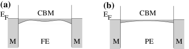
In the centrosymmetric unpolarized reference structure, some metal/ferroelectric interfaces such as BaTiO3/SrRuO3 or PbTiO3/SrRuO3 are “well-behaved” within LDA. [We focus here on the TiO2/SrO termination – the properties of the alternative (Ba,Pb)O/RuO2 termination might differ.] This conclusion emerges from the analysis shown in Fig. 6 for the PbTiO3-based capacitor; qualitatively similar results, not shown here, are obtained for the BaTiO3-based capacitor. Figure 6(a) represents schematically the Schottky barriers for electrons () and holes () at the ferroelectric/metal interfaces, computed using the nanosmoothed electrostatic potential method described in Sec. II.1. The bottom of the conduction band of the ferroelectric lies above the Fermi level of the metal ( amounts to 0.38 eV for the PbTiO3-based capacitor, and only to 0.19 eV in the BaTiO3-based case). Note that, if the experimental band gap could be reproduced in our simulations, would be much larger [dashed lines in Fig. 6(a); we have taken the experimental indirect gap of the cubic phase of PbTiO3, 3.40 eV Peng et al. (1992) and assumed that the quasiparticle correction on the valence band edge is negligible]. The results summarized in Table 2 indicate that, in all the cases discussed here, different methodologies yield Schottky barrier values that are consistent within a few hundredths of an eV. The flatness of the profile of the nanosmoothed electrostatic potential at the central layers of PbTiO3 confirms the absence of any macroscopic electric field, as expected from a locally charge-neutral and centrosymmetric system.

| Capacitor | BS + Lineup | Semicore |
|---|---|---|
| SrRuO3/PbTiO3/SrRuO3 | ||
| (eV) | 0.97 | 0.99 |
| (eV) | 0.38 | 0.37 |
| SrRuO3/BaTiO3/SrRuO3 | ||
| (eV) | 1.39 | 1.41 |
| (eV) | 0.19 | 0.23 |
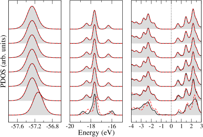
Figure 6(b) displays , as defined in Sec. III.2.1. As expected, has a rapid decay in the insulating layer, consistent with the evanescent character of the metallic states (MIGS): these cannot propagate in the insulator as their energy eigenvalues fall within the forbidden band gap. Fig. 6(c) shows the layer-by-layer polarization, , computed using Eqs. (30)-(32). Consistent with the absence of space charge, the profile is remarkably flat. Due to the imposed mirror-symmetry constraint, also vanishes inside the ferroelectric material.
Fig. 7 shows the layer-resolved PDOS of the Ti(3s) semicore peaks, the O(2s) peak, the upper valence band and the lower conduction band (black curves, shaded in gray). On top of the heterostructure PDOS we superimpose the bulk PDOS, calculated with an equivalent -point sampling and aligned with the Ti(3s) peak (dashed red curves). Note that all PDOS curves were calculated using Eq. (22), and the smearing function of Eq. (23b) with eV, consistent with the parameters used in the calculation. The PDOS of the conduction and valence bands converges fairly quickly to the bulk curve when moving away from the interface – they are practically indistinguishable already at the fourth layer. The estimated energy locations of the conduction and valence bands converge even faster [these are directly related to the shifts of the Ti(3s) state, which are less affected by quantum confinement effects]. All curves except those adjacent to the electrode interface vanish at the Fermi level, confirming the absence of charge spill-out in this system.
As a summary of this Section we can conclude that, when a centrosymmetric unpolarized interface is non-pathological in the sense that the bottom of the conduction band of the ferroelectric is above the Fermi level of the metal, (i) the free charge, as defined in Sec. III.2.1, vanishes due to the absence of charge spill-out; (ii) the local polarization profile (Sec. III.2.3) is perfectly flat as the interface-induced polar lattice distortions heal rapidly (within the first unit cell); (iii) the LDOS/PDOS vanishes at the Fermi level, except for one or two interface layers where the signatures of the MIGS might be still present (they are barely detectable in the curves of Fig. 7).
IV.2 Pathological cases
We analyze now two examples of capacitors that are characterized by a pathological band alignment already in their centrosymmetric reference structure: NbO2-terminated KNbO3/SrRuO3, and TiO2-terminated BaTiO3/Pt. This choice of materials is motivated by the fact that there exist recent theoretical works on these systems, Duan et al. (2006a); Velev et al. (2007) where the consequences of the pathological band alignment were neglected.
IV.2.1 KNbO3/SrRuO3
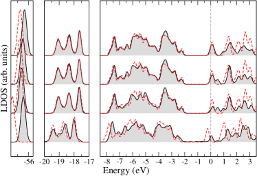
We construct a heterostructure consisting of =6.5 KNbO3 unit cells and =7.5 SrRuO3 cells, for a total of 14 perovskite units; we use symmetrical NbO2 (SrO) terminations of the KNbO3 (SrRuO3) film. After full relaxation with a mirror symmetry constraint at the central NbO2 layer, we perform the analysis of the LDOS, the conduction charge and the local polarization as explained in Sec. III. In Fig. 8 we show the local density of states integrated over the NbO2 layers (the bottom one is adjacent to the electrode interface, the top one lies on the mirror plane in the middle of the film). The unphysical Ohmic band alignment is evident from the location of the conduction band bottom – the whole film is clearly metallic. This points to the pathological situation that is sketched in Fig. 3. Note that the LDOS does not converge to the bulk curve anywhere in the heterostructure. There are non-trivial shifts of all peaks that make it difficult to identify a well-defined alignment with the bulk curves. In Fig. 8 we choose to align the O(2s)-derived feature at eV. In this specific system, aligning the O(2s) peaks appears to yield a reasonably good match of the conduction and valence band edges (the most relevant features from a physical point of view); this, however, leads to a marked mismatch, e.g. in the position of the semicore Nb(4s) state. We show in the following that these effects stem from a number of (rather dramatic) electrostatic and structural perturbations acting on the KNbO3 film, which are a direct consequence of the pathological band alignment.
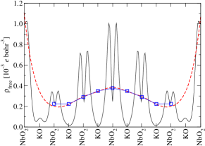
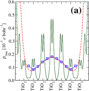
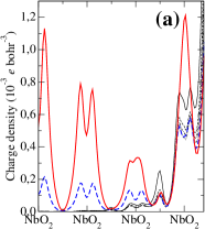
First we show that the non-vanishing LDOS at the Fermi level results in a sizeable spill-out of conduction charge into the ferroelectric film. To that end, we plot , which represents the planar average of the artificially populated part of the KNbO3 conduction band, and the corresponding nanosmoothed version, , in Fig. 9 respectively as black continuous and red dashed lines. The additional electron density in the ferroelectric region is apparent, and reaches a maximum of about 0.15 electrons in the central perovskite unit cell. Such a density is significant – it can be thought as resulting from an unrealistically large doping of, e.g. one Sr2+ cation every six or seven K+ ions. However, unlike in a doped perovskite, the spurious electron spill-out here is not compensated by an appropriate density of heterovalent cations. The system is therefore not locally charge neutral, and as a consequence strong, non-uniform electric fields arise in the insulating film that act on the ionic lattice.
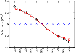
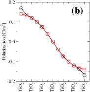
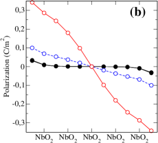
In order to elucidate how the underlying polarizable material responds to such an electrostatic perturbation, we plot in Fig. 10 the effective polarization profile in the KNbO3 film calculated in two ways, (i) the rigorous Wannier-function analysis of the layer polarizations and (ii) the approximate expression based on the renormalized bulk dynamical charges. The matching between the curves is excellent, indicating that the approximate -based formula provides a reliable estimate of ; this suggests that the electrostatic screening is indeed dominated by structural relaxations, as anticipated in Sec. II, and as expected in a ferroelectric material. To substantiate this point, we compare in Fig. 11 the relaxed layer rumplings in KNbO3/SrRuO3 to those of the non-pathological case, PbTiO3/SrRuO3, discussed in Sec. IV.1.
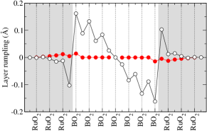
The KNbO3 film is characterized by strong non-homogeneous distortions, which are consistent with the polarization pattern shown in Fig. 10. Conversely, the distortions are negligible in the PbTiO3/SrRuO3 capacitor, where all the oxide layers are essentially flat.
The polarization profile is characterized by a uniform, negative slope. This nicely confirms the prediction of our semiclassical analysis in Sec. II of a uniform linear decrease of throughout the film. varies from 0.3 to -0.3 C/m2 when moving from the bottom to the top interface. Note that such spatial variation is completely absent in, e.g., isostructural paraelectric BaTiO3/SrRuO3 (diamonds in Fig. 10), and PbTiO3/SrRuO3 [Fig. 6(c)] capacitors, where the profile is remarkably flat with vanishing throughout the film. We stress that the non-uniform perturbation experienced by KNbO3/SrRuO3 is qualitatively different from a ferroelectric distortion, which involves an almost perfectly rigid displacement of the ionic sublattices: in absence of space-charge effects, a macroscopically uniform rumpling pattern across the film is typically found. Stengel et al. (2009a)
To demonstrate that the spatial variation in is directly related to according to Eq. (13), we perform a numerical differentiation of the polarization profile derived from the Wannier-based layer polarizations. The result, plotted in Fig. 9 as a blue line, shows an essentially perfect match between and illustrating the fact that the polarization profile is really a consequence of KNbO3 responding to the spurious population of the conduction band, rather than of interface bonding effects. Duan et al. (2006a)
IV.2.2 BaTiO3/Pt
We next present results of an analogous investigation for a paraelectric (BaTiO3)m/(Pt)n capacitor, with and . We consider symmetric TiO2 terminations, with the interfacial O atoms in the on-top positions. (Note that this interface structure is different than the AO-terminated films simulated, e.g. in Refs. Stengel et al., 2009a and Stengel et al., 2009c, where a Schottky-like band offset was found.) We find this interface to have a pathological band alignment, similar to the KNbO3/SrRuO3 case discussed above. The comparative analysis of the bound-charge polarization profile and of the excess conduction charge, shown in Fig. 12, again shows excellent agreement between and the compensating bound charge. The effect is analogous to KNbO3/SrRuO3, with an overall magnitude which is smaller by roughly a factor of two; the polarizations at the two extremes of the film reach values of about 0.15 C/m2.
The almost perfect similarity in behavior between these two chemically dissimilar systems is further proof that the unusual effects described here and in Ref. Duan et al., 2006a – the apparent head-to-head domain wall in the ferroelectric film – have little to do with the bonding at the interface, but are merely a consequence of the artificial charge spill out, as discussed in Sec. II.
Before moving on to the next Section we briefly comment on the physical nature of the conduction charge that spills into the ferroelectric film. In particular, it is important to clarify that the charge densities plotted in Fig. 9 and Fig. 12(a) indeed originate from population of the conduction band of the insulator, and not from metal-induced gap states (MIGS) as some authors have recently argued. Wang et al. (2010) First, all charge density plots show a maximum in the middle of the ferroelectric layer, rather than a minimum, which one would expect if the former hypothesis were true, given the evanescent character of the MIGS. Second, if MIGS were present they would be clearly identifiable in the local density of states; however, the LDOS plotted in Fig. 8 shows no evidence of quantum states lying within the energy gap of the KNbO3 film. Therefore, we must conclude that these are genuine conduction band states, and not MIGS. The maximum of in the middle of the ferroelectric film can be interpreted either as a quantum confinement effect [the lowest-energy solution of the electron-in-a-box problem is indeed a sine function with a shape reminiscent of the plots of Fig. 9 and Fig. 12(a)], and/or as a result of the dielectric nonlinearities discussed in Sec. II.3.3.
IV.3 Estimating the “pre-spill” band offset
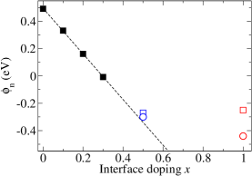
We mentioned in Sec. II that, whenever an electrode/ferroelectric interface enters the pathological spill-out regime, the transfer of charge into the conduction band of the insulator produces an upward shift of the CBM. This effect prevents a direct, unambiguous determination of the interface parameter . To circumvent this problem, and obtain an approximate estimate of the negative “pre-spill” Schottky barrier , we use an approach inspired by a recent work. Burton and Tsymbal (2010) The authors of Ref. Burton and Tsymbal, 2010 show that the Schottky barrier at the interface between a perovskite insulator (SrTiO3) and a perovskite electrode (La0.7A0.3MnO3, where A is Ca, Sr, or Ba) evolves linearly as a function of the compositional charge of the interface layer. (This interface layer is of the type LaxSr1-xO, where interpolates between a +3 and a +2 cation.) Of course, this linear behavior refers to a range of values where the interface is non-pathological; our arguments indicate that as soon as the system enters the spill-out regime, the value of saturates to a nearly constant value. Based on this observation, if one knows the linear behavior of in a range of values for which the interface is non-pathological, one can extrapolate this straight line to the values of which cannot be directly calculated, and obtain an estimate for .
We apply this strategy to the same KNbO3/SrRuO3 capacitor system described in Sec. IV.2.1. To tune the interface charge, we replace the Sr cation in the interface SrO layer with a fictitious atom of fractional atomic number . corresponds to the example already shown in Sec. IV.2.1, with a charge-neutral SrO interface layer, and corresponds to a RbO layer of net formal charge -1. The results for the Schottky barrier are plotted in Fig. 13. The region from to is non-pathological and shows an almost perfectly linear evolution of (dashed line). By extrapolating this linear trend to we obtain eV, which is about 1 eV lower than the value calculated from first principles. This confirms the remarkable impact of the space-charge effects described in Sec. II.3.1. Assuming a polarization of C/m2 for KNbO3 near the interface, a potential drop of 1 eV would be accounted for by an effective screening length of 0.3 Å at the electrode interface. This value is quite reasonable, and similar in magnitude to those reported in Table 1 .
In order to examine the crossover between the Schottky (non-pathological) and the Ohmic (pathological) regimes in terms of the analysis tools developed in this work, we plot in Fig. 14 the polarization profiles and the density of conduction electrons for each of the calculations summarized in Fig. 13. These plots confirm that from to the capacitors are non-pathological, with absence of conduction charge in the insulating region [panel (a), thinner lines] and a flat polarization profile [panel (b), filled circles – all these curves overlap on this scale]. Conversely, at the conduction band starts populating significantly [thicker dashed blue line in (a), empty blue circles in (b), note that the corresponding points in Fig. 13 starts to depart from the linear regime]. At population of the conduction band has become dramatic, and so is the corresponding slope in the polarization profile. The departure from linearity in Fig. 13 is correspondingly large. Note that the use of either the Nb(4s) or the O(2s) semicore peaks in Eq. (24) yields identical results in the non-pathological regime (the filled squares and circles overlap in Fig. 13). Conversely, the result depends significantly on this (completely arbitrary) choice at , and even more so at (the circles and squares split). This is another proof that in the pathological regime the band lineup is ill-defined – due to the electrostatic effects discussed throughout this work, the LDOS does not converge to a bulk-like value in the center of the KNbO3 film (see Fig. 8), and there is no obvious reference energy to determine the offset.
V Results: Ferroelectric capacitors
As discussed in the Introduction, although some of the unpolarized reference structures (e.g. the PbTiO3/SrRuO3 interface) appear artifact-free within LDA, because of the strong dependence of the Schottky barrier on [Eq. 9] they might become problematic when the constraint of mirror symmetry is lifted and the system is polarized. To address this issue, in this section we first use the fixed- strategy described in Sec. III.3 to explore the behavior of the PbTiO3/metal interface over a wide range of polarization states. Then, we will demonstrate that the behavior that we calculate using the fixed- method corresponds exactly to that of a true short-circuited capacitor by performing more “standard” large-scale calculations for a few selected thickness values.
V.1 Open-circuit calculations
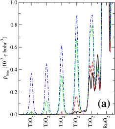
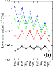
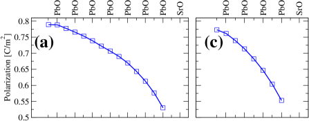
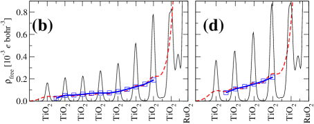
We construct a vacuum/PbTiO3/SrRuO3 heterostructure as explained in Sec. III.3. The reduced macroscopic displacement field Stengel et al. (2009b), , is controlled by substituting the Ti at the PbTiO3/vacuum interface with a fictitious cation of atomic number (i.e. Zr for =0). The thickness of the PbTiO3 slab is set to 5 unit cells, and that of SrRuO3 to 4; other computational parameters are kept the same as in the rest of this work. We considered four different values of : 0.2, 0.4, 0.6 and 0.74, the latter one corresponding to the ferroelectric ground state of PbTiO3 at the SrTiO3 in-plane lattice constant. In each case, we verify by examining the LDOS that the free surface remains locally insulating; therefore, the macroscopic in the film corresponds exactly to the value enforced by the artificial pseudopotential.
The evolution of and of the Wannier-based layer polarization profiles for is shown in Fig. 15. It is apparent from the plots of that already for the smallest value of the polarization [, black curve in Fig. 15(a)] the TiO2 layer closest to the electrode has an important density of conduction electrons. This is expected, as the evanescent tails of the metal-induced gap states (MIGS) penetrate into the insulating region for some distance at any metal/insulator junction. However, these states do not propagate very far, and already at the second TiO2 layer they are barely noticeable on the scale of the plot. At [red curve in Fig. 15(a)] the peak on the second TiO2 layer significantly increases in magnitude, and a new small peak appears at the third TiO2 layer. Analysis of the local density of states (not shown) shows that these new peaks are conduction band states of PbTiO3, rather than evanescent SrRuO3 states. The reason why decays relatively fast when moving into the insulator is due here to the internal field in PbTiO3, which generates a confining wedge-like potential. We stress again that this mechanism is fundamentally different from the usual quantum-mechanical damping of the MIGS that fall in a forbidden energy window of the insulator. We identify this mechanism with the onset of the Schottky breakdown, which becomes increasingly apparent if the polarization of the film is further increased to [green curve in Fig. 15(a).] As in the discussion of the paraelectric capacitors, the presence of the space charge is reflected in the progressive “bending” of the layer polarization profile [Fig. 15(b)].
At , the population of the conduction band becomes rather dramatic, and the charge distributes over the whole film. Here, the space charge is no longer confined by the depolarizing field: in the fully polarized ferroelectric state the internal field of PbTiO3 vanishes. Therefore, the intrinsic carriers are only loosely bound to the interface by the band bending effect, analogous to the mechanism that confines the compensating carriers at the LaAlO3/SrTiO3 interface. Stengel (2010) Since the dielectric permittivity of PbTiO3 is rather large, the band bending is very efficiently screened, and the distribution of charge can reach quite far into the insulator. To demonstrate this fact, we have repeated the simulation with the same value of =0.74, but with a thicker PbTiO3 film of 8 unit cells [Fig. 16 (b)]; indeed, the conduction electrons redistribute over the whole volume of the film to minimize their kinetic energy. Thus, in close analogy to the LaAlO3/SrTiO3 case, the metallization of the fully polarized PbTiO3 film at =0.74 can be thought as a form of “electrostatic doping” induced by spill-out of electrons from the electrode to the PbTiO3 conduction band. We shall further elaborate on this point in Sec. VI.6.
Fig. 15(b) illustrates a further important consequence of the charge spill-out regime, which was mentioned already in Sec. II.3.2: in the pathological regime the dipoles that lie closest to the electrode interface may appear “pinned” to a fixed value. This is indeed the case for the TiO2 layer adjacent to the electrode, which seems to saturate at nC/m for increasing values of . Again, we caution against interpreting this dipole pinning effect as a robust physical result.
V.2 Short-circuit calculations
To demonstrate in practice that the conclusions of Sec. V.1, inferred by using open-circuit boundary conditions, are directly relevant to short-circuited capacitors, we have performed simulations on SrRuO3/PbTiO3 heterostructures, with = 12.5 and = 5.5. A soft-mode distortion of the bulk tetragonal phase, inducing a polarization perpendicular to the interface, is superimposed on the PbTiO3 layers of the previous unpolarized configurations discussed in Sec. IV.1. Then the atomic positions of all the ions, both in the ferroelectric and in the metallic electrodes, and the out-of-plane stress are relaxed again with the same convergence criteria as before.
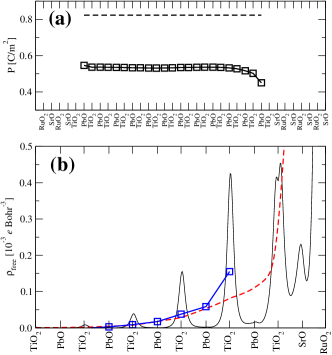
By means of the approximate Eq. (33), derived in Sec. III.2.3, we computed the local layer-by-layer polarization, , plotted in Fig. 17 (a). Far enough from the interface, the polarization profile is rather uniform, with a polarization that amounts to 0.53 C/m2 in PbTiO3 (64 % of the strained bulk polarization), which we identify as the macroscopic of the PbTiO3 film. This corresponds to , i.e. a value that in the open-circuit study of the previous section (see Fig. 15) we found to be already pathological. To verify that the same happens here, we analyze the density of conduction electrons. The planar average of for the relaxed polar configuration is plotted in Fig. 17(b). The existence of a charge populating the Ti orbitals is evident from the peaks of at the TiO2 layers, which are detectable up to four unit cells away from the interface. Indeed the profile of the conduction charge appears to be intermediate between the and cases of Sec. V.1, consistent with the present estimate .
As we already anticipated in the previous Sections, is responsible for non-trivial lattice relaxations, which act to screen the electrostatic perturbation. Fig. 17(a) indeed shows a small bending of the local polarization profile, starting roughly three unit cells away from the top interface and with a negative slope of the local polarization, . To prove that such a spatial variation of [which in PbTiO3 provides a reasonably accurate estimate of the local electric displacement ] is a direct consequence of the presence of the non-vanishing conduction charge [recall Eq. (13)], we numerically differentiatiate the polarization profile and compare it with in Fig. 17(b). As in the SrRuO3/KNbO3/SrRuO3 unpolarized case (see Fig. 9), the bound charge (divergence of ) accurately neutralizes the conduction charge (nanosmoothed profile of ).
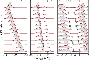
In order to further prove that the present case fits into the model description of Sec. II.3.2, in Fig. 18 we plot the layer-resolved PDOS. The curves were constructed exactly as in Fig. 7, except that (i) the capacitor is now polarized; and (ii) consistent with the discussion of Sec. III.1.3 we set up the bulk reference calculation by using the PbTiO3 structure extracted from the polarized supercell calculation (i.e. with atomic distortions and out-of-plane strain consistent with a polarization of 0.53 C/m2). The agreement is again very good, showing that our approximation of neglecting the macroscopic depolarizing field in the bulk reference calculation is a reasonable one, and that the most important effects on the LDOS originate from the lattice distortions. In the capacitor we clearly distinguish two regions. In the lower part of the PbTiO3 film, the PDOS at the Fermi level vanishes, which implies that the system is locally insulating. Furthermore, the PDOS in each layer appears rigidly shifted with respect to the neighboring two layers, consistent with the presence of a depolarizing field. In the upper region, close to the top electrode, the PDOS crosses the Fermi level and the system is locally metallic. All these features are in full agreement with the scheme drawn in Fig. 4.
In Fig. 18 we also plot the estimated band edges for each layer, , obtained from Eq. (24). We used the semicore Ti(3s) peak at each layer as , and we calculated the bulk contributions in Eq. (24) from a non-self-consistent bulk calculation (based on the ground state charge density of the bulk reference calculation at 0.53 C/m2 described above) that included the high-symmetry -points. The resulting data points lie very accurately on a straight line. By extrapolating this straight line, we see that it crosses the Fermi level near the fourth PbTiO3 cell from the top electrode interface. This illustrates the pathological character of the band alignment in this system, consistent with the model of Fig. 4.
As a final remark, we mention that we performed similar calculations for a polarized BaTiO3/SrRuO3 capacitor, and found a very similar scenario, with the conduction band locally crossing the Fermi level as the mirror symmetry plane is lifted and a spontaneous polarization is allowed to develop. In general, the onset of such a pathological regime has important consequences on many physical properties of the capacitor, as we shall discuss in the following Section.
VI Discussion
In this Section we discuss the important aspects of our work in the context of the existing literature. The discussion is organized in several categories, corresponding to the different properties of a ferroelectric/electrode interface (or, more generally, of a perovskite material) that might be affected by the (more or less spurious) presence of free charges in the system.
VI.1 Structural properties of the film
The authors of Ref. Duan et al., 2006a studied KNbO3 thin films placed between symmetric metallic electrodes (either SrRuO3 or Pt) under short-circuit electrical boundary conditions. In the SrRuO3 case, the layer-by-layer polarization pointed in opposite directions at the top and bottom interfaces for all thicknesses, creating 180∘ head to head domain walls, which were denominated interface domain walls (IDW). The physical origin of the IDW was attributed to a strong bonding between interfacial Nb and O atoms, which would induce a “pinning” of the interface dipoles to opposite values at the top and bottom electrode interfaces.
Here we have demonstrated with analytical derivations and practical examples that both the inhomogeneous polarization and the “dipole pinning” effect are clear signatures of a pathological band alignment. In particular, in an unpolarized KNbO3/SrRuO3 capacitor analogous to those simulated by Duan et al. Duan et al. (2006a), we obtain a monotonously decreasing polarization profile, from (0.3 C/m2) at the bottom interface to an opposite value of -0.3 C/m2 at the top, in excellent agreement with the results of Duan and coworkers.Duan et al. (2006a) In contrast with the conclusion of Ref. Duan et al., 2006a, however, here we find that the microscopic origin of this strong inhomogeneous polarization is the spillage of charge from the metallic electrode to the bottom of the conduction band of KNbO3, rather than a bonding effect.
These findings have important consequences concerning the physical understanding of the system with regard to the relevant observables. First, the ferroelectric material becomes in fact a metal, and such a device would respond Ohmically with a large direct DC current that would make switching difficult or impossible. This questions the appropriateness of interpreting the “average” polarization of the film as a macroscopic physical quantity that can be measured in an experiment (see next Section). Second, our arguments indicate that two essential factors governing the equilibrium free charge distribution (and hence the spatial variation of ) are the conduction band structure (e.g. the density of states) of the ferroelectric material, and the interface band offset. Both ingredients are absent in traditional Landau-Ginzburg models, e.g. those used in Ref. Duan et al., 2006a to interpret the above data on KNbO3/SrRuO3 capacitors, or in Ref. Wang et al., 2010 to interpret qualitatively similar results for a hole-doped BaTiO3/SrRuO3 interface. We therefore caution against overinterpreting the results of such models, as they might fail at capturing the relevant physics of the free-charge equilibration. A promising route towards overcoming these limitations appears to be the model Hamiltonian approach proposed in Ref. Stengel, 2010. Extending that strategy to the case of a metal/ferroelectric interface will be an interesting subject of further research.
VI.2 Stability of the ferroelectric state
The pathological spill-out of charge has important consequences on the spontaneous polarization of a ferroelectric capacitor. To give a qualitative flavor of such an effect, we consider the case of a capacitor that is only partially metallic, i.e. there is a depolarizing field that keeps the carriers confined to the pathological side as sketched in Fig. 19(a). We further consider two symmetric electrodes, i.e. characterized by identical values of (that we assume positive) and . Assuming a monodomain state, there are then two stable configurations, related by a mirror symmetry operation. As is positive, upon application of an electric field there will always be an insulating region in the middle of the film, i.e. the polarization can be switched without passing through a globally metallic state.
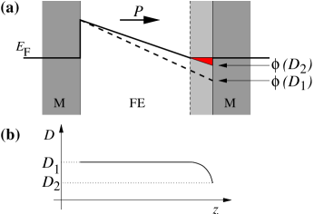
To appreciate the impact of the charge spill-out on the spontaneous polarization of the film, it is useful to look at the schematic band diagram of Fig. 19(a), where the conduction band bottom goes below the Fermi level in proximity of the right electrode (red area). This induces metallicity in a significant portion of the film (light grey shaded area, up to the dashed line). Based on our arguments of Sec. II, the charge spill-out is associated with a spatially decreasing [Fig. 19(b)]. This, in turn, modifies the interface potential barrier by producing a strong upward shift in energy of the conduction band edge from what one would have if were uniform and equal to the “physical” value . This implies that the charge spill out generally reduces the depolarizing field [the “pre-spill” estimate is sketched as a thick dashed line in Fig. 19(a)], and hence overstabilizes the ferroelectric state. This is what one intuitively expects – population of the conduction band constitutes an additional channel for screening the polarization charge, and this cooperates with the metallic carriers of the electrode. This, however, contrasts with the conclusions of Ref. Wang et al., 2010, where it was argued that charge leakage suppresses by producing a ferroelectrically “dead” layer. These conclusions are based on the assumption that the physically measurable is the average polarization, , taken over the whole volume of the film. As the polarization is locally reduced near a pathological interface, charge spill-out indeed results in a reduced .
Is it justified, though, to assume that is the physically relevant quantity in the capacitor? Does , in other words, reflect what is experimentally measured? In an experiment one measures the time integral of the transient current density, , that flows through the capacitor during the switching process. does not relate to . Under the hypothesis that at least a portion of the film remains insulating throughout switching, it rigorously follows from the modern theory of polarization Resta and Vanderbilt (2007) that ; is the value of the (locally uniform) electric displacement deep in the insulating region, indicated as in Fig. 19. (We assume for simplicity that in the paraelectric reference state.) Therefore, observing that is reduced upon charge leakage does not reflect the true physical effect of the pathological band alignment, which is an artificial enhancement of the spontaneous via the reduction of the depolarizing field illustrated above.
A large number of works Sai et al. (2005); Umeno et al. (2006); Al-Saidi and Rappe (2010); Umeno et al. (2009) have investigated the stability of PbTiO3-based capacitors, and it is impossible here to discuss in detail whether and how the above band-alignment issues might have affected each of them (for instance, regarding the polarization enhancements reported in Ref. Sai et al., 2005). We limit ourselves to observe that, due to the large spontaneous polarization of PbTiO3, the possible consequences of having a pathological ferroelectric state need to be taken seriously into account in the analysis, as we showed for the example of SrRuO3 electrodes in Sec. V.
VI.3 Transport properties in the tunneling regime
Ferroelectric capacitors have been explored as potential tunneling electroresistance devices,Zhuravlev et al. (2005) and many recent calculations focused on the calculation of the conductance by means of first-principles methods. Metallicity and spill-out of electrons is a serious potential issue in this context, as the calculated conductance can potentially be affected by the presence of space charge in the system, in a way which is difficult to predict. The recent work of Velev et al. Velev et al. (2007) appears to be concerned by these issues, as it focuses on TiO2-terminated Pt/BaTiO3/Pt capacitors. Indeed, we find (see Sec. IV.2.2) that this interface is problematic already in the centrosymmetric paraelectric case. While we have not explored the ferroelectric regime in this system, based on the imperfect screening arguments of Sec. II (the lineup depends linearly on around the paraelectric reference phase) we expect the spill-out effect to become worse at least at one of the two interfaces when the capacitor is polarized.
In fact, the metallicity of the ferroelectric film seems to be confirmed by the data presented by the authors: In Fig. 2(a-b) of Ref. Velev et al., 2007 the conduction band minimum (CBM) of the central BaTiO3 cell appears to be degenerate or lower than the Fermi level, and in Fig. 1 of the same paper the atomic displacements of the ferroelectric phase seems to be strongly asymmetric, consistent with our speculations. While we cannot draw a definitive conclusion (our computational setup slightly differs from that of Ref. Velev et al., 2007), our analysis highlights the crucial importance of the band alignment issue, and the necessity of performing an adequate and convincing assessment of its impact on the results (e.g. the conductance) in each case.
VI.4 Interface magnetoelectric effects
Magnetoelectricity is one of the emerging topics in oxide research. Despite the intense efforts, one of the main limiting factors still persists: bulk materials displaying a robust magnetoelectric effect are notoriously difficult to find. To work around this problem, several researchers have been looking for alternative solutions by exploring heterostructures and composite materials. An interface, due to its lower symmetry, might allow for physical response properties that are absent in the parent compounds. A promising route to interfacial ME coupling that has been proposed recently Rondinelli et al. (2008) is mediated by charge. The polarization of the ferroelectric (or dielectric) lattice produces a bound charge at the interface, that is screened by the carriers of the metal. If these carriers are spin-polarized, as in a ferromagnet, there will be a net change in the magnetization.
It is easy to see that the band-alignment issues that we discuss in this work have direct and important implications for the calculation of the carrier-mediated interface ME coefficient. In the pathological regime, the calculated (magnetic) response will most likely be suppressed, as the spill-out charge, rather than the spin-polarized carriers in the electrode, will screen the applied bias potential (or the ferroelectric polarization). This speculation is directly relevant for interpreting the results of Yamauchi et al.Yamauchi et al. (2007) on BaTiO3 films sandwiched between Co2MnSi (Heusler alloy) electrodes. Depending on the termination, two qualitatively different behaviors were reported: the MnSi/TiO2 interface results in a pathological band alignment and a strongly non-homogeneous local polarization profile; conversely, neither is present in the capacitor with the other type of termination, which has symmetric Co/TiO2 interfaces. A very small magnetoelectric response was reported for the MnSi/TiO2 case (contrary to the Co/TiO2 case), in qualitative agreement with our arguments above.
Other recent studies,Fechner et al. (2008, 2010) focusing on ME effects in thin Fe film deposited on ATiO3 (A=Ba,Pb,Sr), also reported strongly non-uniform polarization profiles in the ferroelectric film (e.g. Fig. 3 of Ref. Fechner et al., 2010). This suggests that also the ATiO3/Fe interface might be concerned by the band-alignment issues discussed in this work, with potential impact on the physical observables. Our analysis tools should help clarify these issues in the above systems and in the Fe/BaTiO3/Fe capacitors of Ref. Duan et al., 2006b.
VI.5 Schottky barriers
Direct calculations of Schottky barriers at metal/ferroelectric interfaces are, among the many useful physical properties of these junctions, those that are most directly affected by the issues we discuss here. The consequence of a pathological band alignment is that the estimated Schottky barrier is no longer a physically meaningful interface property, but is influenced by macroscopic space-charge phenomena.
A rather comprehensive work on the SrTiO3/transition metal interface was recently reported in Ref. Mrovec et al., 2009. Without going into too detailed an analysis of the results, we limit ourselves to noting that many of the reported -type SBH for TiO2- or SrO-terminated interfaces are very close to, or sometimes well in excess of 1.8 eV. Considering that the LDA/GGA fundamental gap of SrTiO3 is around 1.8 eV, the actual -type SBH of the calculation (i.e. not the value corrected with the experimental band gap) is close to zero or negative. Therefore, charge spill out is a concrete and likely possibility for many of the investigated structures.
Note that, contrary to the case of oxide electrodes, ideal interfaces between SrTiO3 and simple metals tend to have a smaller . Stengel and Spaldin (2006) This implies that the effects of the electrostatic re-equilibration described in Sec. II might be somewhat less dramatic, and the values of the self-consistent closer to . This suggests that the trends and the conclusions reported in Ref. Mrovec et al., 2009 are likely to be robust with respect to the issues described in this work. However, a more detailed analysis would be certainly interesting in order to assess their impact at the quantitative level.
VI.6 Relationship to LaAlO3/SrTiO3
Many of the analysis tools developed in this work are not limited to ferroelectric capacitors, but can be readily extended to other systems where free-charge doping of a band insulator plays a central role. An excellent example, where the interpretation of the observed effects is still widely debated, is two dimensional conducting electron gas (2DEG) that forms at the polar LaAlO3/SrTiO3 interface. Ohtomo and Hwang (2004) A central problem is the determimation of the physical effects governing the confinement and equilibrium distribution of the 2DEG. Some authorsJanicka et al. (2009) propose a mechanism for the confinement of the gas based on the formation of metal induced gap states (MIGS) in the band gap of SrTiO3. Other authors,Copie et al. (2009) however, explain the experimental observations in terms of a semiclassical Thomas-Fermi model that is analogous to that described in Sec. II, and where the MIGS are completely absent. Answering the question of whether the MIGS play an important role in this system involves a careful analysis of the local electronic properties, and more specifically of the LDOS. Janicka et al. (2009) In this sense, the methodology discussed in Sec. III.1.3 appears ideally suited to clarifying this issue.
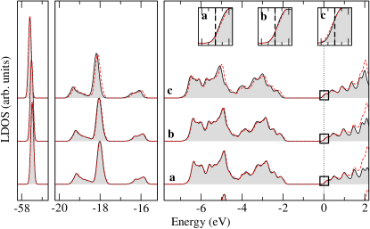
We base our analysis on the calculations done in Ref. Stengel, 2010, with a 24-cell thick SrTiO3 slab and a 3-cell LaAlO3 overlayer. (This calculation was performed with a Monkhorst-Pack sampling of the surface Brillouin zone, and with a Gaussian smearing of 0.1 eV; full details of the computational parameters are reported in Ref. Stengel, 2010.) The boundary conditions are set to =0, , and are equivalent to those of the symmetric superlattice used by Janicka et al. Janicka et al. (2009) In Fig. 20 we show the LDOS corresponding to the TiO2 layers number 15 (curve a), 10 (b) and 5 (c), where layer 1 is adjacent to the LAO interface. On top of each curve we superimpose the bulk TiO2 LDOS, that we align with the supercell LDOS by matching the semicore Ti peak at eV. (As in earlier works the O peak was used as a reference, we also show the O-derived feature, which is located at about -18 eV.) The matching is excellent in all cases, especially in the layers lying furthest from the interface where the effect of the structural distortions and free charge are less pronounced. (Note that we performed the bulk calculation with a -point mesh that accurately matches the one used in the supercell calculation. Also, in the construction of the LDOS curves we used the same Gaussian smearing function of width 0.1 eV, corresponding to the smearing used to relax the self-consistent ground state of the supercell structure.) In the insets we show a blow-up of the conduction band edge, which goes below the Fermi energy in agreement with the semiclassical arguments of Ref. Copie et al., 2009 and of our Sec. II. Clearly, our plots do not show any evidence for MIGS in the energy gap, contrary to the conclusions of Janicka et al. Janicka et al. (2009)
To reconcile this discrepancy, we can speculate that the LDOS curves presented in Ref. Janicka et al., 2009 might have been constructed with a substantially larger smearing width than ours, and this might have precluded an accurate identification of the band edges. We believe that the technique presented here (of superimposing an appropriately constructed bulk LDOS on top of the supercell curves) provides a very practical means of minimizing systematic errors in the analysis of the results.
VII Conclusions
Due to its accuracy and efficiency, density functional theory has emerged as the method of choice for studying ferroelectric oxides from first-principles. This predominance has been reinforced since the early 1990s by the many successes achieved in the determination of the structural, energetic, piezoelectric, and dielectric properties at the bulk level. In the last few years, those efforts have evolved to address the behaviour of the functional properties in thin films and superlattices, including in same cases (for instance, in the study of ferroelectric capacitors) the presence of metal/insulator interfaces.
For a reliable prediction of the functional properties of these devices, the atomic displacements, distortions of the unit cell, the electronic structure and the band gap have to be accurately described simultaneously. However, the proper DFT treatment of such interfaces is complicated by the so-called “band-gap problem”, which might produce a pathological alignment between the Fermi level of the metal and the conduction band of the insulator, thus precluding explicit DFT investigation of many systems of practical interest. In this work we provide useful guidelines to identify such a pathological scenario in a calculation by examining its main physical consequences: (i) an inhomogeneous polar distortion propagating into the bulk of the film, (ii) the film becoming partially or totally metallic due to a non-vanishing free charge, and (iii) the local conduction band edge crossing the Fermi level. The above three effects are intimately linked, and should be considered as potential artifacts of the aforementioned band-gap problem. Whenever one of these “alarm flags” is raised in a calculation, the results should be examined with great caution.
A route to overcoming this limitation involves correcting the LDA/GGA bandgap while preserving the excellent accuracy of these functionals in the prediction of ground-state properties. Traditional methods to increase the band gap of insulators, like the inclusion of a Hubbard term in the Hamiltonian, are not satisfactory in the case of a ferroelectric capacitor with B-cation driven ferroelectricity. A more promising avenue has been recently opened by Bilc et al. Bilc et al. (2008) and Wahl and coworkers, Wahl et al. (2008) using the so-called “hybrid” functionals that combine Hartree-Fock exchange and DFT. In particular the B1-WC functional proposed in Ref. Bilc et al., 2008 has been shown to provide good structural, electronic and ferroelectric properties as compared to experimental data for BaTiO3 and PbTiO3; verifying the accuracy of B1-WC in interface studies will be an interesting subject for future research. Unfortunately, the price to pay for this accuracy is the substantially higher computational cost of B1-WC compared to LDA/GGA.
In addition to the purely technical issues, our work also opens interesting avenues regarding fundamental physical concepts. For example, ferroelectricity is usually understood within the modern theory of polarization, which is only applicable in the absence of conduction electrons (i.e. in pure insulators at zero electronic temperature). It is an important fundamental question, therefore, to assess whether our understanding of ferroelectrics in terms of bound charges, polarization and macroscopic electrical quantities still applies (and to what extent) in a regime where a sizable amount of space charge is present in the system. This issue is of crucial importance also for other systems, e.g. electrostatically doped perovskites, which bear many analogies to the physical mechanisms discussed in this work. The first-principles-based modeling approach proposed in Ref. Stengel, 2010 appears to be a promising route to further exploring this interesting topic.
VIII Acknowledgements
The authors are indebted to Ph. Ghosez and A. Filippetti for useful discussions. This work was supported by the Spanish Ministery of Science and Innovation through the MICINN Grant FIS2009-12721-C04-02 (JJ); by the Spanish Ministry of Education through the FPU fellowship AP2006-02958 (PAP); by DGI-Spain through Grants No. MAT2010-18113 and No. CSD2007-00041 (MS); by the European Union through the project EC-FP7, Grant No. NMP3-SL-2009-228989 “OxIDes” (JJ and MS); and by the US National Science Foundation, award number DMR-0940420 (NAS). JJ, PAP and MS thankfully acknowledge the computer resources, technical expertise and assistance provided by the Red Española de Supercomputación. Calculations were also performed at the ATC group of the University of Cantabria, and at CESGA.
Appendix A Local polarization via Born effective charges
In this Appendix we discuss the approach, used in several parts in this manuscript and ubiquitously in the recent literature, of associating the local value of the “effective” polarization (i.e. the induced with respect to the reference centrosymmetric configuration Resta and Vanderbilt (2007)) in capacitor heterostructures with an approximate formula, based on the Born effective charges, . In particular, we provide formal justification for an improved formula, still based on the , that we introduced in this work, and we already mentioned in Sec. III.2.3.
Recall the definition of the approximate effective polarization in terms of the Born effective charges in a bulk solid,
| (36) |
It is easy to verify that the layer-resolved expression of Eq. (32) reduces to in the case of a periodic crystal, where is a constant function of the layer index . does not reduce to the “correct” polarization at any value of , as it does not take into account the additional polarization of the electronic cloud due to the internal field (recall that the Born effective charges are defined under the condition of zero macroscopic electric field. Ghosez et al. (1998))
| BaTiO3 | -48.87 | 6.48 | 0.90 |
|---|---|---|---|
| PbTiO3 | -96.54 | 8.33 | 0.93 |
| KNbO3 | -34.92 | 6.27 | 0.87 |
Taking the Taylor expansion of the polarization as a function of (we assume for simplicity that , and all vanish in the reference centrosymmetric structure), we can write
| (37) |
For small values of , we can truncate the previous expansion at the linear order term. Now, by definition
| (38) |
where is the lattice-mediated susceptibility, and
| (39) |
where is the total dielectric constant of the insulator (relative to the vacuum permittivity ). Substituting Eq. (38) and Eq. (39) into Eq. (37)
| (40) |
The same kind of arguments applied to the total polarization yield
| (41) |
where is the sum of the lattice-mediated susceptibility, , and the purely electronic (frozen-ion) susceptibility, . Note that is not bound to be positive. In a ferroelectric material, for example, the centrosymmetric reference structure is unstable and therefore yields a negative (and hence ), as discussed in Ref. Stengel et al., 2009b. The present derivation is general and encompasses those cases.
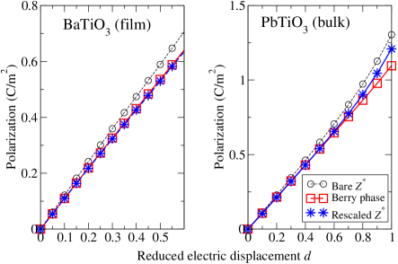
From the above considerations it immediately follows that an estimate of the total polarization, which is exact in the linear limit, can be given as
| (42) |
This is essentially Eq. (33). In practice, and are calculated in the reference phase according to the standard definitions, Gonze and Lee (1997)
| (43) |
where is a unit mass, are the normal mode charges and are the eigenvalues of the dynamical matrix, and
| (44) |
The values of these physical constants that are relevant for the results presented in this manuscript are reported in Table 3.
We proceed in the following to test this approximation on two representative bulk ferroelectric materials, PbTiO3 and BaTiO3. We take the relevant data (linear susceptibilities, Born charges and relaxed structures as a function of ) from the calculations of Ref. Stengel et al., 2009b and Ref. Stengel et al., 2009a. Note that the BaTiO3 calculation was performed at a fixed value of the in-plane lattice parameter (indicated as “film” in the figure) while in the PbTiO3 calculation both and parameters were relaxed for each value of . The results are presented in Fig. 21. In both cases, the “bare” value is systematically overestimated compared to the Berry-phase polarization. With the correction described above, i.e. by rescaling all values by the factor , the approximate value of accurately matches the Berry-phase one. The accuracy is surprisingly good in BaTiO3, where the maximum deviation is of the order of 1%. In PbTiO3, for large values of the rescaled- value of presents significant deviations. Note that these deviations mostly concern values of that are larger than that of the ferroelectric ground state (), and therefore are not of concern in this manuscript. We ascribe these deviations to the field-induced structural transition that was described in Ref. Stengel et al., 2009b.
In conclusion, this simple rescaling factor appears to be an effective way to obtain a relatively accurate value of the local in heterostructure calculations, based only on the local atomic positions and a few ingredients that can be easily computed in the bulk reference structure. From the results of our tests, we expect the agreement to be best in cases where the polarization is small (closer to the linear limit where the approximation becomes exact). Furthermore, cases where the ferroelectric polarization can be represented in terms of a single “soft mode” such as BaTiO3 seem to work better than cases, like PbTiO3, where significant mode mixing and non-trivial structural transitions occur at higher values.
Appendix B Convolutions and energy smearing of the local density of states
B.1 Convolutions
Convolution is a mathematical operation on two functions and , producing a third function that is typically viewed as a modified version of one of the original functions. For the purpose of the present notes, it is useful to think of as a data curve containing the relevant physical information, and as a rapidly-decaying “smoothing” function that produces a local weighted average of . We define the convolution of and , , as the following integral transform,
| (45) |
Convolutions have many properties, including commutativity and associativity. Furthermore, the Dirac delta can be thought as the identity under the convoluton operation,
| (46) |
and under certain assumptions an inverse operation can also be defined. In other words, the set of invertible distributions forms an abelian group under the convolution.
A particularly useful property holds in relationship to the Fourier transform,
| (47) |
where denotes the Fourier transform of , and is a constant that depends on the normalization convention for the Fourier transform. Thus, in reciprocal space the convolution becomes a simple product. This naturally provides an efficient convolution algorithm: the workload is reduced from to .
B.2 Local density of states
In this work we use [Eq. (22)] the following formula to compute the smeared local density of states (LDOS),
| (48) |
We shall see that this is indeed a convolution. We first get rid of the spatial cordinates. To this end, it is customary to integrate the LDOS in real space over a given volume ,
| (49) |
where
| (50) |
(Note that sometimes it might be more convenient to use a projected density of states, rather than a local density of states. In such cases it is sufficient to replace the real-space integral in the above equation with an appropriate sum over angular momentum components. The following discussion remains unchanged.) Now the LDOS is a function of a single energy variable. If we write
| (51) |
we can easily see that . This leads to a simple reciprocal-space expression. We first define an energy window, , that contains the entire eigenvalue spectrum . We actually take a window which is slightly larger, where this “slightly” depends on the decay properties of ,
| (52) |
The width of this window is . We represent in reciprocal space as a discrete Fourier transform,
| (53) |
where and is an integer. By using Eq. (47) we have
| (54) |
The Fourier transform of a Dirac delta centered in the origin is a constant. Eq. (54) then decomposes the local density of states into a structure factor,
| (55) |
and a form factor . Obviously, this formulation is only convenient if the function has a fast decay in both real and reciprocal space, so that the sum in Eq. (53) can be truncated. This is indeed the case for the most widely used smoothing functions , as we shall see in the following.
B.3 Gaussian vs. Fermi-Dirac smearing
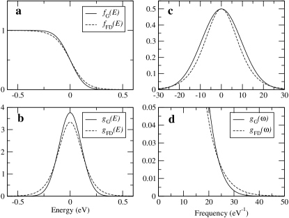
The Gaussian smearing (G) and the Fermi-Dirac (FD) smearing are by far the most popular choices for the occupation function in first-principles calculations of metallic systems. If we define the occupation function as the integral of a “kernel” function ,
| (56) |
one can verify that the Gaussian or Fermi-Dirac occupation are, respectively, reproduced by the following choices of ,
| (57) | |||||
| (58) |
where is the smearing energy [these correspond to Eq. (23a) and Eq. (23b)]. It is easy to see that, by combining Eq. (57) or Eq. (58) with Eq. (56) one obtains the standard definitions of the occupation function (we assume that the complementary error function, erfc, values 2 at ),
| (59) | |||||
| (60) |
It is useful to spell out the explicit formulas for the Fourier transforms of both smearing functions,
| (61) | |||||
| (62) |
Note that the above formulas are normalized according to the conventions on the Fourier transforms that we used in the previous section. The functions and defined above are shown in Fig. 22. Note that a different choice of was used in the Fermi-Dirac and in the Gaussian case. A FD distribution is roughly equivalent to a G distribution with a value that is twice as large.
In the main text and here we have assumed that it is a good idea to use the same kernel in the calculation and in the construction of the LDOS. We shall substantiate this point in the following Section.
B.4 On the optimal choice of
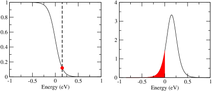
In many cases, the specific choice of the function to be used in Eq. (48) is largely arbitrary. Typically, the goal is to filter out the unphysical wiggles due to the discretization of the -mesh, but at the same time to preserve the main physical features, without blurring them out completely. This calls for a smearing function that is neither too sharp nor too broad. Since a “slightly too broad” or a “slightly too sharp” smearing function usually does not influence the physical conclusions, in many cases one has the freedom of choosing whatever yields the clearest visual aid to support the discussion.
There are cases, however, where this choice is not just a matter of aesthetics, and using the “wrong” function can qualitatively and quantitatively influence the interpretation of the results. More specifically, the issue concerns cases where the analysis of the LDOS (or DOS or PDOS) is used to detect and quantify the population of orbitals that lie close in energy to the Fermi level. As we focus on charge spill-out phenomena that concern the conduction band of a dielectric/ferroelectric film in contact with a metallic electrode, this is a central point of our work. The problem is most easily appreciated by looking at the left panel of Fig. 23. There is a single orbital lying at an energy of 0.15 eV above the Fermi level. As this orbital lies above the Fermi level, one might be tempted to think that the orbital is empty, and that charge spill-out does not occur at all. However, calculations in metallic systems are routinely performed by using an occupation function that is artificially broadened, in order to improve convergence of the ground-state properties; in Fig. 23 we assume a Fermi-Dirac occupation with a fictitious electronic temperature of 0.075 eV. It is easy to see that with such an occupation function, the orbital lying at 0.15 eV won’t be empty, but will be “thermally” populated by tail of the Fermi-Dirac distribution. The final result is a charge transfer of 0.119 electrons into this orbital.
Now, is there a “right” way to construct the DOS curve, such that the above-mentioned charge transfer could be qualitatively and quantitatively inferred from the DOS, without knowing any further detail of the calculation? The answer is yes, and consists in constructing the DOS by using as broadening function which is consistent with the occupation function used by the code. In this case, this is , with a identical to that used to calculate the electronic ground state. To demonstrate this point, we plot in the right panel of Fig. 23 the DOS of this isolated orbital at 0.15 eV, appropriately convoluted with . Eq. (56) guarantees that, by doing this, one recovers the very intuitive result that the total amount of electron charge, , present in the volume (over which the LDOS was integrated) exactly corresponds to the integral of the DOS up to the Fermi level,
| (63) |
Then, a simple look at the DOS curve is sufficient to ascertain whether a significant transfer of charge has occurred into a specific group of bands. As this rigorous sum rule can be very practical in the analysis of the results, we encourage a systematic use of the “internally consistent” LDOS construction described above.
References
- Scott and de Araujo (1989) J. F. Scott and C. A. P. de Araujo, Science 246, 1400 (1989).
- Auciello et al. (1998) O. Auciello, J. F. Scott, and R. Ramesh, Physics Today July, 22 (1998).
- Scott (2000) J. F. Scott, Ferroelectric memories (Springer-Verlag, 2000).
- Dawber et al. (2005) M. Dawber, K. M. Rabe, and J. F. Scott, Rev. Mod. Phys. 77, 1083 (2005).
- Scott (2006) J. F. Scott, J. Phys.: Condens. Matter 18, R361 (2006).
- Scott (2007) J. F. Scott, Science 315, 954 (2007).
- Fiebig (2005) M. Fiebig, J. Phys. D: Appl. Phys. 38, R123 (2005).
- Eerenstein et al. (2006) W. Eerenstein, N. D. Mathur, and J. F. Scott, Nature (London) 442, 759 (2006).
- Ahn et al. (2003) C. H. Ahn, J. Mannhart, and J.-M. Triscone, Nature (London) 424, 1015 (2003).
- Tsymbal and Kohlstedt (2006) E. Y. Tsymbal and H. Kohlstedt, Science 313, 181 (2006).
- Maksymovych et al. (2009) P. Maksymovych, S. Jesse, P. Yu, R. Ramesh, A. Baddorf, and S. V. Kalinin, Science 324, 1421 (2009).
- García et al. (2009) V. García, S. Fusil, K. Bouzehouane, S. Enouz-Vedrenne, N. Mathur, A. Barthélémy, and M. Bibes, Nature (London) 460, 81 (2009).
- García et al. (2010) V. García, M. Bibes, L. Bocher, S. Valencia, F. Kronast, A. Crassous, X. Moya, S. Enouz-Vedrenne, A. Gloter, D. Imhoff, et al., Science 327, 1106 (2010).
- Ghosez and Junquera (2006) P. Ghosez and J. Junquera, in Handbook of Theoretical and Computational Nanotechnology, edited by M. Rieth and W. Schommers (American Scientific Publisher, Stevenson Ranch, CA, 2006).
- Junquera and Ghosez (2008) J. Junquera and P. Ghosez, J. Comput. Theor. Nanosci. 5, 2071 (2008).
- Souza et al. (2002) I. Souza, J. Íñiguez, and D. Vanderbilt, Phys. Rev. Lett. 89, 117602 (2002).
- Umari and Pasquarello (2002) P. Umari and A. Pasquarello, Phys. Rev. Lett. 89, 157602 (2002).
- Souza et al. (2004) I. Souza, J. Íñiguez, and D. Vanderbilt, Phys. Rev. B 69, 085106 (2004).
- Stengel and Spaldin (2007) M. Stengel and N. A. Spaldin, Phys. Rev. B 75, 205121 (2007).
- Stengel et al. (2009a) M. Stengel, D. Vanderbilt, and N. A. Spaldin, Phys. Rev B 80, 224110 (2009a).
- Perdew and Levy (1983) J. P. Perdew and M. Levy, Phys. Rev. Lett. 51, 1884 (1983).
- Sham and Schlüter (1983) L. J. Sham and M. Schlüter, Phys. Rev. Lett. 51, 1888 (1983).
- Stengel and Spaldin (2006) M. Stengel and N. A. Spaldin, Nature (London) 443, 679 (2006).
- Junquera and Ghosez (2003) J. Junquera and P. Ghosez, Nature (London) 422, 506 (2003).
- Zhuravlev et al. (2005) M. Y. Zhuravlev, R. F. Sabirianov, S. S. Jaswal, and E. Y. Tsymbal, Phys. Rev. Lett. 94, 246802 (2005).
- Heine (1965) V. Heine, Phys. Rev. 138, A1689 (1965).
- Okamoto and Millis (2004) S. Okamoto and A. J. Millis, Nature 428, 630 (2004).
- Baldereschi et al. (1988) A. Baldereschi, S. Baroni, and R. Resta, Phys. Rev. Lett. 61, 734 (1988).
- Colombo et al. (1991) L. Colombo, R. Resta, and S. Baroni, Phys. Rev. B 44, 5572 (1991).
- Junquera et al. (2007) J. Junquera, M. H. Cohen, and K. M. Rabe, J. Phys.: Condens. Matter 19, 213203 (2007).
- Franciosi and de Walle (1996) A. Franciosi and C. G. V. de Walle, Surface Science Reports 25, 1 (1996).
- Stengel et al. (2009b) M. Stengel, N. A. Spaldin, and D. Vanderbilt, Nature Physics 5, 304 (2009b).
- Stengel et al. (2009c) M. Stengel, D. Vanderbilt, and N. A. Spaldin, Nature Materials 8, 392 (2009c).
- Stengel (2010) M. Stengel, arXiv:1012.2468 (2010).
- Peressi et al. (1998) M. Peressi, N. Binggeli, and A. Baldereschi, J. Phys. D: Appl. Phys. 31, 1273 (1998).
- (36) In practical simulations, the origin of the -point grid may be displaced from = 0 in order to decrease the number of inequivalent -points. Monkhorst and Pack (1976); Moreno and Soler (1992) This shift usually prevents the appearance of high-symmetry points from the list of -points used during the self-consistent procedure or in the calculations of the density of states.
- (37) The band gap of both BaTiO3 and PbTiO3 is indirect, with the top of the valence band located at in BaTiO3 and at in PbTiO3, and the bottom of the conduction band at in both materials.
- Delaney et al. (2010) K. T. Delaney, N. A. Spaldin, and C. G. Van de Walle, Phys. Rev. B 81, 165312 (2010).
- Bardeen and Shockley (1950) J. Bardeen and W. Shockley, Phys. Rev. 80, 72 (1950).
- Fall et al. (1999) C. J. Fall, N. Binggeli, and A. Baldereschi, J. Phys.: Condens. Matter 11, 2689 (1999).
- Grigoriev et al. (2008) A. Grigoriev, R. Sichel, H. N. Lee, E. C. Landahl, B. Adams, E. M. Dufresne, and P. G. Evans, Phys. Rev. Lett. 100, 027604 (2008).
- Wu et al. (2006) X. Wu, O. Diéguez, K. M. Rabe, and D. Vanderbilt, Phys. Rev. Lett. 97, 107602 (2006).
- Murray and Vanderbilt (2009) E. D. Murray and D. Vanderbilt, Phys. Rev. B 79, 100102 (2009).
- Marzari and Vanderbilt (1997) N. Marzari and D. Vanderbilt, Phys. Rev. B 56, 12847 (1997).
- Neaton and Rabe (2003) J. B. Neaton and K. M. Rabe, Appl. Phys. Lett. 82, 1586 (2003).
- Stengel and Vanderbilt (2009) M. Stengel and D. Vanderbilt, Phys. Rev B 80, 241103 (2009).
- Soler et al. (2002) J. M. Soler, E. Artacho, J. D. Gale, A. García, J. Junquera, P. Ordejón, and D. Sánchez-Portal, J. Phys.: Condens. Matter 14, 2745 (2002).
- Payne et al. (1992) M. Payne, M. Teter, D. Allan, T. Arias, and J. Joannopoulos, Rev. Mod. Phys. 64, 1045 (1992).
- Blöchl (1994) P. E. Blöchl, Phys. Rev. B 50, 17953 (1994).
- Monkhorst and Pack (1976) H. J. Monkhorst and J. D. Pack, Phys. Rev. B 13, 5188 (1976).
- Moreno and Soler (1992) J. Moreno and J. M. Soler, Phys. Rev. B 45, 13891 (1992).
- Kleinman and Bylander (1982) L. Kleinman and D. M. Bylander, Phys. Rev. Lett. 48, 1425 (1982).
- Troullier and Martins (1991) N. Troullier and J. L. Martins, Phys. Rev. B. 43, 1993 (1991).
- Junquera et al. (2003) J. Junquera, M. Zimmer, P. Ordejón, and P. Ghosez, Phys. Rev. B 67, 155327 (2003).
- Peng et al. (1992) C. H. Peng, J. F. Chang, and S. Desu, MRS Symp. Proc. 243, 12 (1992).
- Duan et al. (2006a) C.-G. Duan, R. F. Sabirianov, W.-N. Mei, S. S. Jaswal, and E. Y. Tsymbal, Nano Letters 6, 483 (2006a).
- Velev et al. (2007) J. P. Velev, C.-G. Duan, K. D. Belashchenko, S. S. Jaswal, and E. Y. Tsymbal, Phys. Rev. Lett. 98, 137201 (2007).
- Wang et al. (2010) Y. Wang, M. K. Niranjan, K. Janicka, J. P. Velev, M. Y. Zhuravlev, S. S. Jaswal, and E. Y. Tsymbal, Phys. Rev. B 82, 094114 (2010).
- Burton and Tsymbal (2010) J. D. Burton and E. Y. Tsymbal, Phys. Rev. B 82, 161407 (2010).
- Resta and Vanderbilt (2007) R. Resta and D. Vanderbilt, in Physics of Ferroelectrics: A Modern Perspective, edited by K. M. Rabe, C. H. Ahn, and J.-M. Triscone (Springer-Verlag, Berlin Heidelberg, 2007).
- Sai et al. (2005) N. Sai, A. M. Kolpak, and A. M. Rappe, Phys. Rev. B 72, 020101(R) (2005).
- Umeno et al. (2006) Y. Umeno, B. Meyer, C. Elsässer, and P. Gumbsch, Phys. Rev. B 74, 060101(R) (2006).
- Al-Saidi and Rappe (2010) W. A. Al-Saidi and A. M. Rappe, Phys. Rev. B 82, 155304 (2010).
- Umeno et al. (2009) Y. Umeno, J. M. Albina, B. Meyer, and C. Elsässer, Phys. Rev. B 80, 205122 (2009).
- Rondinelli et al. (2008) J. M. Rondinelli, M. Stengel, and N. A. Spaldin, Nature Nanotechnology 3, 46 (2008).
- Yamauchi et al. (2007) K. Yamauchi, B. Sanyal, and S. Picozzi, Appl. Phys. Lett. 91, 062506 (2007).
- Fechner et al. (2008) M. Fechner, I. V. Maznichenko, S. Ostanin, A. Ernst, J. Henk, P. Bruno, and I. Mertig, Phys. Rev. B 78, 212406 (2008).
- Fechner et al. (2010) M. Fechner, I. V. Maznichenko, S. Ostanin, A. Ernst, J. Henk, and I. Mertig, Phys. Status Solidi B 247, 1600–1607 (2010).
- Duan et al. (2006b) C.-G. Duan, S. S. Jaswal, and E. Y. Tsymbal, Phys. Rev. Lett. 97, 047201 (2006b).
- Mrovec et al. (2009) M. Mrovec, J.-M. Albina, B. Meyer, and C. Elsässer, Phys. Rev. B 79, 245121 (2009).
- Ohtomo and Hwang (2004) A. Ohtomo and H. Y. Hwang, Nature 427, 423 (2004).
- Janicka et al. (2009) K. Janicka, J. P. Velev, and E. Y. Tsymbal, Phys. Rev. Lett. 102, 106803 (2009).
- Copie et al. (2009) O. Copie, V. Garcia, C. Bödefeld, C. Carrétéro, M. Bibes, G. Herranz, E. Jacquet, J.-L. Maurice, B. Vinter, S. Fusil, et al., Phys. Rev. Lett. 102, 216804 (2009).
- Bilc et al. (2008) D. I. Bilc, R. Orlando, R. Shaltaf, G.-M. Rignanese, J. Íñiguez, and P. Ghosez, Phys. Rev. B 77, 165107 (2008).
- Wahl et al. (2008) R. Wahl, D. Vogtenhuber, and G. Kresse, Phys. Rev. B 78, 104116 (2008).
- Ghosez et al. (1998) P. Ghosez, J.-P. Michenaud, and X. Gonze, Phys. Rev. B 58, 6224 (1998).
- Gonze and Lee (1997) X. Gonze and C. Lee, Phys. Rev. B 55, 10355 (1997).