Effect of current hysteresis on the spin polarization of current in a paramagnetic resonant tunneling diode
Abstract
A spin-dependent quantum transport is investigated in a paramagnetic resonant tunneling diode (RTD) based on a Zn1-xMnxSe/ZnBeSe heterostructure. Using the Wigner-Poisson method and assuming the two-current model we have calculated the current-voltage characteristics, potential energy profiles and electron density distributions for spin-up and spin-down electron current in an external magnetic field. We have found that – for both the spin-polarized currents – two types of the current hysteresis appear on the current-voltage characteristics. The current hysteresis of the first type occurs at the bias voltage below the resonant current peak and results from the accumulation of electrons in the quantum well layer. The current hysteresis of the second type appears at the bias voltage above the resonant current peak and is caused by the creation of the quasi-bound state in the left contact region and the resonant tunneling through this quasi-bound state. The physical interpretation of both the types of the current hysteresis is further supported by the analysis of the calculated self-consistent potential profiles and electron density distributions. Based on these results we have shown that – in certain bias voltage and magnetic field ranges – the spin polarization of the current exhibits the plateau behavior with the nearly full spin polarization. This property is very promising for possible applications in spintronics.
pacs:
72.25.Dc, 85.30.MnI Introduction
A rapid progress in homo- and heteroepitaxy of semiconductors with magnetic dopants Ohno1992 ; Ohno1998 ; Hayashi2001 ; Edmonds2002 ; Yu2002 ; Chiba2003 ; Ku2003 ; Eid2005 ; Jungwirth2005 has led to the interest in the transport properties of the diluted magnetic semiconductors (DMSs) due to their potential spintronic applications. A special attention is paid to the studies of (Zn,Mn)Se Furdyna1988 ; Yu1995 and (Ga,Mn)As.Ando2003 ; Liu2005 ; Jungwirth2006 ; Dietl2001 . The nanostructures consisting of the non-magnetic and magnetic layers Gruber2001 ; Slobodskyy2003 ; Beletskii2003 lead to a possibility of creation of the nanodevice, in which spin polarization of the current can be controlled by the bias voltage. The fabrication of an effective spin filter for application to semiconductor spintronic nanodevices, such as spin transistor Datta1990 , is one of the most important challenge for the contemporary nanotechnology.
The application of DMS nanostructure as an effective spin filter has been first proposed by Egues. Egues1998 The nanostructure studied in Ref.Egues1998 consisted of a paramagnetic semiconductor layer made of Zn1-xMnxSe, sandwiched between two non-magnetic ZnSe layers. In the presence of the external magnetic field, the giant Zeeman effect occurring in the Zn1-xMnxSe layer Furdyna1988 causes that the paramagnetic layer acts as a potential well for spin-down electrons and as a potential barrier for spin-up electrons, which leads to the total current dominated by the spin-down electrons. In this type of the nanodevice, the spin polarization of the current can be controlled by the external magnetic field. There is another type of the nanodevice, namely, the resonant tunneling diode (RTD) with the paramagnetic quantum well, in which the spin polarization of the current can be controlled by the bias voltage in the presence of the external magnetic field. If the magnetic field is applied to the paramagnetic RTD, the resonant tunneling conditions are satisfied for the different bias voltages for the spin-up and spin-down electrons due to the giant Zeeman splitting of the quasi-bound state in the paramagnetic quantum well. This leads to the separation of the corresponding resonant current peaks and consequently to the spin polarization of the current. The paramagnetic RTD based on the ZnBeSe/ZnMnSe heterostructure was experimentally demonstrated by Slobodskyy et al., Slobodskyy2003 and theoretically investigated by Havu et al. Havu2005 In both the experimental and theoretical studies, the separation of the resonant current peaks corresponding to the different spin components of the current was found. Nevertheless, in these studies, we did not find any hint for a current hysteresis and its influence on the spin polarization of the current. On the other hand, the nonlinear effects, in particular, the current hysteresis (current bistability), can be observed in the resonant tunneling through the nanodevices made from the non-magnetic materials.Goldman1987 ; Sheard1988 ; Sollner1987 The first observation of the current hysteresis in the nonmagnetic (AlGa)As/GaAs/(AlGa)As heterostructure was reported by Goldman and Tsui.Goldman1987 The current hysteresisGoldman1987 occurs in the negative differential resistance (NDR) region of the current-voltage characteristics and is attributed to the accumulation of the electrons in the quantum well layer.Sheard1988 Sollner Sollner1987 proposed another explanation of the current bistability based on the oscillations of a circuit containing an element that exhibits the NDR. In non-magnetic RTDs, the following two types of the current hysteresis can be distinguished: (I) the hysteresis occurring in the bias voltage range below the resonant current peak Su1991 ; Macks1996 , (II) the hysteresis occurring in the bias voltage range above the resonant current peak.Goldman1987b Moreover, one can observe both the types of hysteresis on the same current-voltage characteristics (double hysteresis).Goldman1987 Recently, Dai et al. Dai2006 have investigated a possibility of tuning the current hysteresis in the non-magnetic resonant tunneling diode by changing the geometric parameters of the nanodevice and found that the increase of the collector barrier width can enhance the current hysteresis of type (I), while the decrease of the collector barrier width enhances the type (II) current hysteresis. These results Dai2006 indicate that the geometric parameters considerably affect the nonlinear transport properties of the nanodevice.
However, in the paramagnetic RTD, the current hysteresis and its influence on the spin polarization of the current has not been studied until now. In this paper we present the results of such investigations. We show that the current hysteresis is of crucial importance for obtaining the spin-polarized current. We provide the physical interpretation of this effect based on the analysis of the self-consistent potential profile and the electron density distribution. We have predicted the bistable behavior of the spin current polarization as a function of the bias voltage and the appearance of plateaus of the spin current polarization as a function of the external magnetic field.
The paper is organized as follows: in Sec. 2, we describe the model of paramagnetic RTD and the self-consistent Wigner-Poisson method. Section 3 contains the results, Section 4 – the discussion, and Section 5 – the conclusions and summary.
II Model and Theory
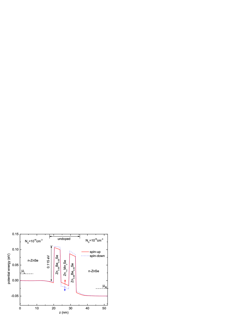
We consider the paramagnetic RTD diode consisting of the Zn1-xMnxSe paramagnetic layer sandwiched between the two Zn0.95Be0.05Se layers (Fig. 1). The active region of the nanodevice is separated from -doped ZnSe contacts by two spacer layers located at the left and right contacts. The difference between the conduction band minima of Zn1-xMnxSe and Zn0.95Be0.05Se leads to the potential energy profile with two barriers and one quantum well, in which the quasi-bound states can be formed. We focus on the effect of bias voltage applied between the left and right contacts and the external magnetic field applied in the growth direction on the spin polarization of the current. In the presence of the magnetic field, the exchange interaction between the spins of the Mn2+ ions and the spins of the conduction band electrons leads to the giant Zeeman splitting of the conduction band minima in the paramagnetic quantum well.Furdyna1988 This splitting occurs at temperatures below the Curie temperature of Zn1-xMnxSe and gives rise to the different potential energy profiles for spin-up and spin-down electrons. For the small concentration of Mn2+ ions the giant Zeeman splitting can be expressed by the formulaFurdyna1988
| (1) |
where eV is the sp-d exchange constant for the conduction band electrons,Twardowski2005 is the concentration of Mn2+ ions, is the effective Brillouin function for spin that corresponds to the spin of Mn2+ ion, is the effective Landé factor, is the Bohr magneton, and are the phenomenological parameters accounting for Mn-Mn interaction that are chosen as follows:Yu1995 and K for , while and K for .
The potential energy profiles for the spin-up and spin-down electrons in the nanodevice are displayed in Fig. 1.
We calculate the current-voltage characteristics of the paramagnetic RTD using the modified version of the self-consistent Wigner-Poisson approach. For this purpose we extend our previous approachWojcik2010 by assuming the two-current model,bookZiman2000 ; Spisak2009 according to which the conduction band electrons are described by the spin-dependent Wigner distribution function (WDF). In order to calculate the electronic transport through the nanodevice we apply the simplified version of the quantum kinetic equation.Weng2003 ; Spisak2005 ; Spisak2009 Assuming the translational invariance in the plane, the quantum transport equations for the steady state can be reduced to the following one-dimensional form:
| (2) |
where is the spin-dependent WDF, is the -component of the wave vector, is the electron conduction band mass, and is the electron spin index.
The non-local Wigner potential for spin channel is given by the formula
where is the total spin-dependent potential energy that consists of the two terms: conduction band potential energy and Hartree potential energy .
At this stage of our study, we neglect the exchange interaction between the conduction band electrons. The conduction band potential energy has the form
where is the position of the barrier/well (paramagnetic/non-magnetic) interface, is the Heaviside step function, is the height of the -th barrier and is the giant Zeeman splitting of the conduction band in the paramagnetic layer.
In Eq. (II), the Zeeman splitting for the conduction band electrons has been neglected because it is a few orders of magnitude smaller than the giant Zeeman splitting occurring in the paramagnetic quantum well.
The Hartree potential energy satisfies the Poisson equation
| (5) |
where is the vacuum electric permittivity, is the relative static electric permittivity, and is the concentration of the ionized donors.
The density of the electrons with spin can be expressed as follows:
| (6) |
Quantum kinetic equation (2) and Poisson equation (5) constitute a system of equations that can be solved by a self-consistent numerical procedure.Kim2007 We assume the Dirichlet boundary conditions for the Poisson equation, i.e., and , where is the bias voltage applied between the left (L) and right (R) electrodes separated by distance .
When solving quantum kinetic equation (2) we use the open boundary conditionsFrensley1990 in the form
| (7) | |||||
where is the supply functionbookFerry2009 that for contact has the form
| (8) |
where is the temperature, and is the electrochemical potential of reservoir .
The current density for non-interacting spin channels can be expressed by the following formula:
| (9) |
We note that although the right-hand side of Eq. (9) contains coordinate , the current is independent of for the steady state solution. The present calculations have been performed with the geometric parameters of the nanodevice, for which the most pronounced current hysteresis has been found in non-magnetic RTD.Dai2006 We have checked that – in the paramagnetic RTD – the current hysteresis effects are also the strongest for the same geometry as in nonmagnetic RTD. In the nanodevice studied in the present paper, the contacts are made from the -type ZnSe with the homogeneous ionized donor concentration cm-3, the thickness of each contact is equal to 17 nm, the thickness of each spacer layer is 3 nm, the thickness of each potential barrier (well) layer is 3 nm (5 nm), the total length of the nanodevice nm, and the height of the potential barrier eV.Chauvet2000 The energy of the left-contact conduction band bottom is taken as the reference energy and set equal to 0. Due to the small thickness of the double-barrier region we assume that the electrons are described by the conduction band effective mass of ZnSe, i.e., , where is the free electron mass. We take on the relative electric permittivity and the lattice constant nm for ZnSe. The present simulations have been carried out for temperature K. We have applied the computational grid with mesh points for coordinate and mesh points for wave vector .
III Results
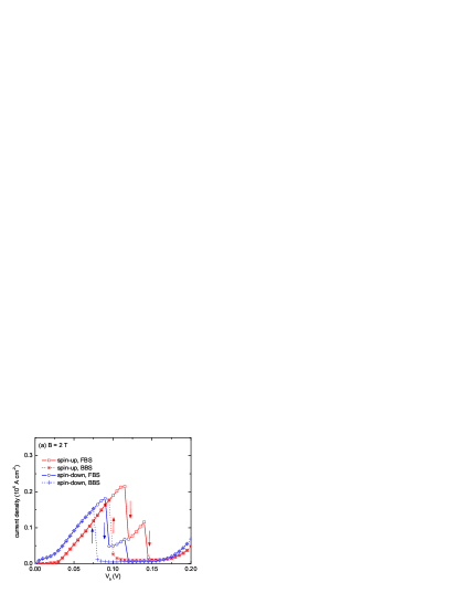
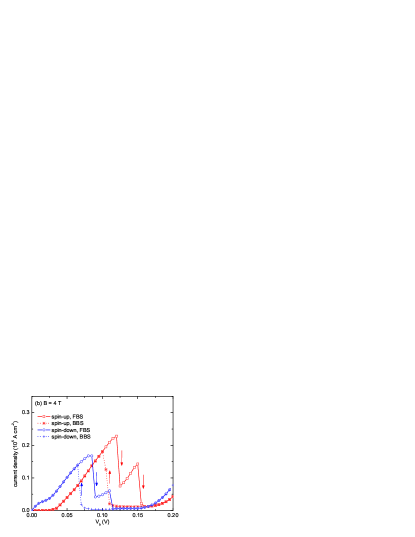
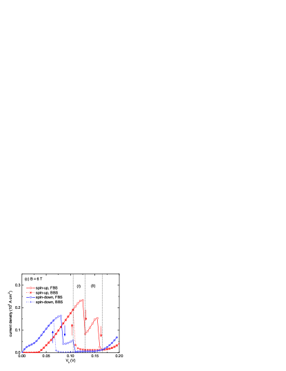
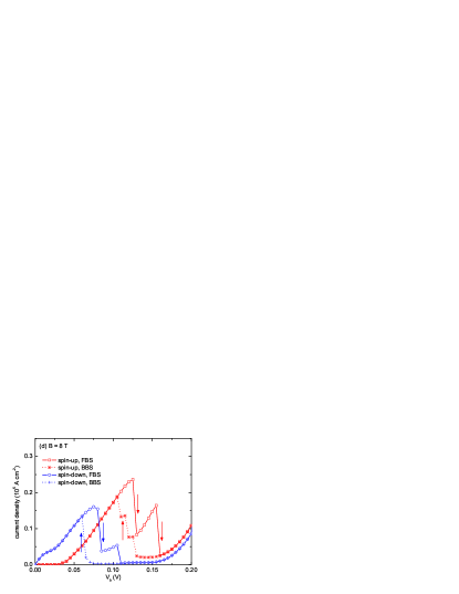
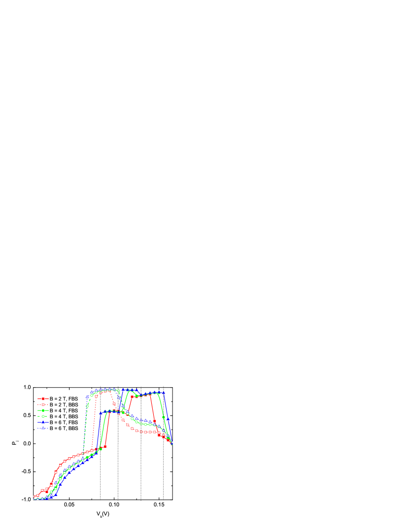
Using the steady state Wigner-Poisson approach, described in Sec. II, we have performed calculations of current-voltage characteristics for the paramagnetic RTD in the presence of external magnetic field for the spin-up and spin-down current components, separately. Each of these characteristics have been obtained for the two directions of the bias sweep: forward bias sweep (FBS), in which the bias voltage increased from V to V with step V and backward bias sweep (BBS), in which the bias voltage decreased from V to V with step V. In Fig. 2, we present the calculated current-voltage characteristics for different values of the magnetic fields.
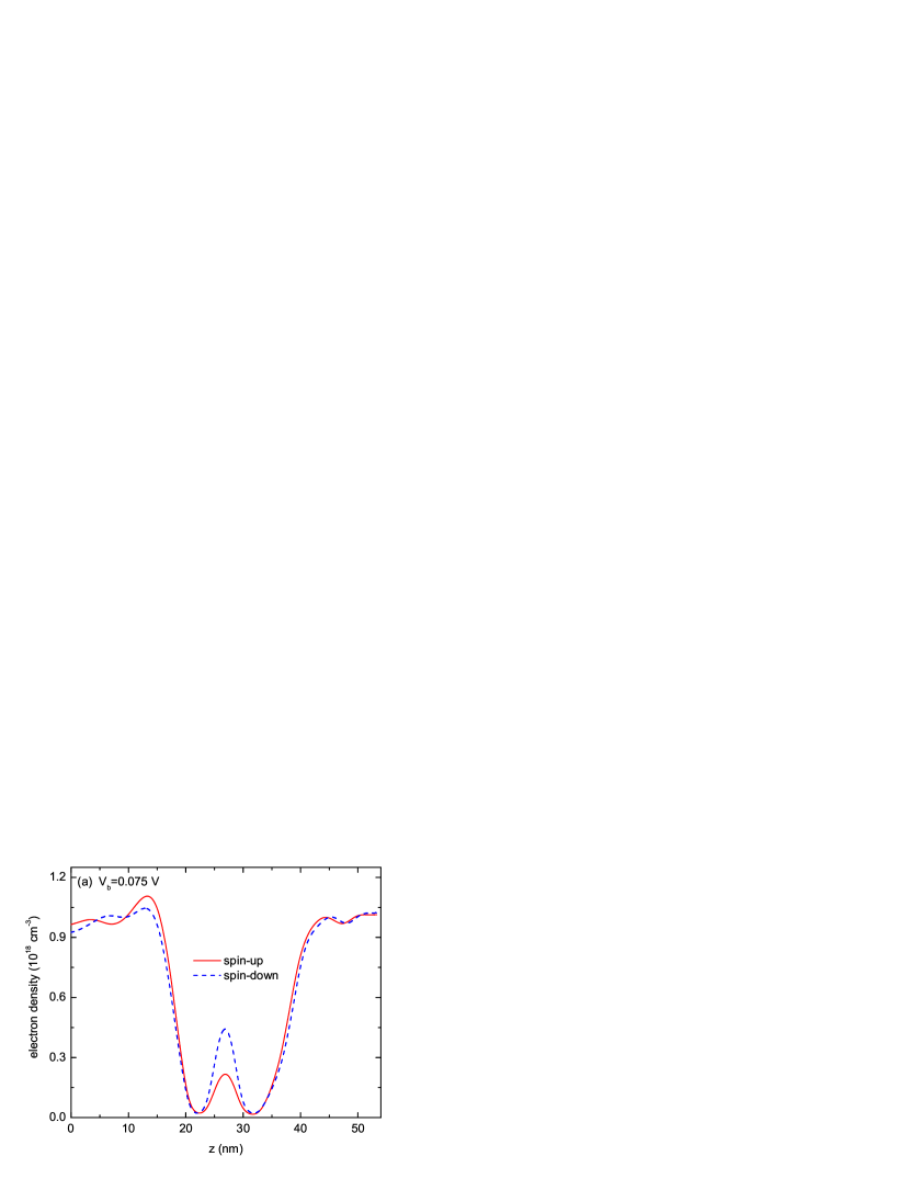
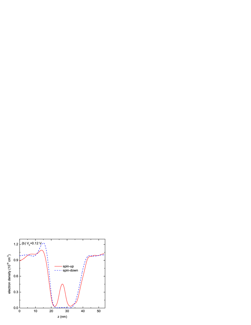
The results of Fig. 2 show that the resonant current peaks corresponding to the spin-up and spin-down current components for FBS and BBS are separated. The separation of the resonant current peaks results from the giant Zeeman splitting of the energy levels corresponding to the quasi-bound states formed in the paramagnetic quantum well and increases with the increasing magnetic field. This means that the resonance conditions for the spin-up and spin-down electron currents are satisfied for the different values of the bias voltage. In order to get a more deep physical insight into this effect, we present in Fig. 3 the spin-dependent electron density for magnetic field T in the case of FBS and for the following two values of the bias voltage: V [Fig. 3 (a)] that corresponds to the current peak for spin-down current component and V [Fig. 3 (b)] that corresponds to the current peak for spin-up current component. The larger accumulation of the spin-down electrons in the quantum well [Fig. 3(a)] indicates that the resonance condition is better satisfied for these electrons. In Fig. 3(b), the electron density distributions for spin-up and spin-down electrons are completely different in the quantum well layer. In this case, we have obtained the fairly high concentration of spin-up electrons with a simultaneous almost complete depletion of spin-down electrons in the quantum well. This electron density distribution corresponds to the resonance conditions satisfied for the spin-up electrons only.
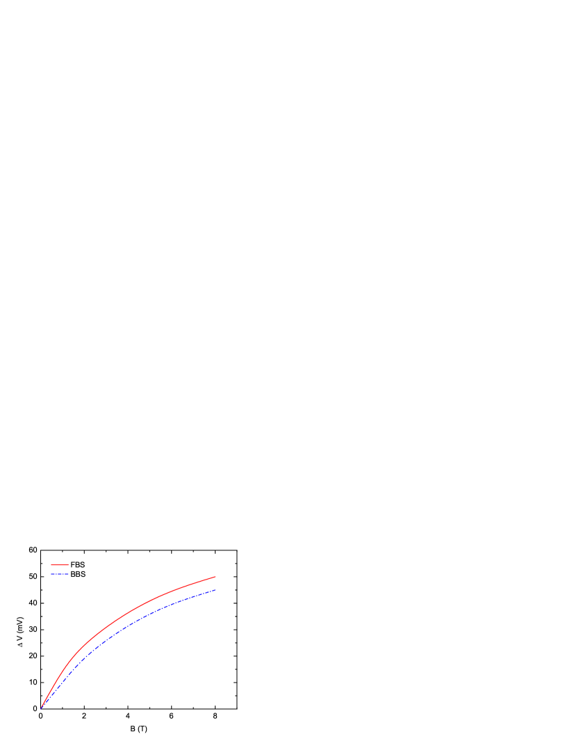
The results plotted in Figs. 2(a-d) show that the increasing magnetic field shifts the position of the current maximum for the spin-up current component towards the higher values of the bias voltage, while the position of the current maximum for the spin-down current component is shifted towards the lower values of the bias voltage. Fig. 4 displays the separation between the resonant current peaks for the spin-up and spin-down current components as a function of magnetic field. The separation between these peaks increases with the increasing magnetic field and reaches mV at T. For each value of the magnetic field for BBS is lower than that for FBS.
The efficiency of the spin filter is characterized by the spin polarization of the current defined as follows:
| (10) |
where and are the current densities for the spin-up and spin-down electrons, respectively.
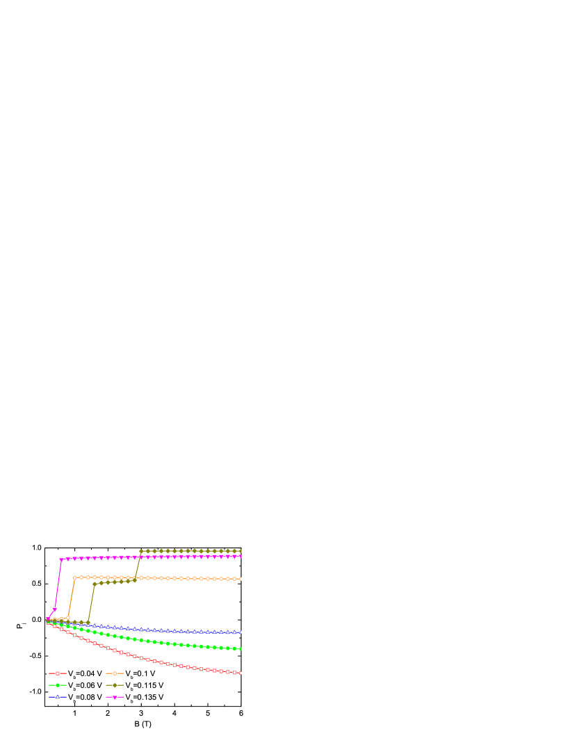
Fig. 2 shows that the current-voltage characteristics for the spin-up and spin-down current components obtained for the increasing bias (FBS) essentially differ from those obtained for the decreasing bias (BBS). This leads to the hysteresis that occurs for each spin component of the current. These hysteresis loops and the phenomena responsible for them determine the current polarization. The calculated spin current polarization is depicted in Fig. 5 as a function of bias voltage, and Fig. 6 as a function of magnetic field. We observe the distinct plateau regions of the spin current polarization that appear for certain bias voltage (Fig. 5) and magnetic field (Fig. 6). In some ranges of the bias voltage and magnetic field, we have obtained almost full spin polarization of the current flowing through the paramagnetic RTD. The different spin current polarization obtained for FBS and BBS [Fig. 5] results from the current hysteresis (cf. Fig. 2). For example, for V and T the spin current polarization in the case of the BBS but in the case of the FBS. Fig. 5 shows that the spin current polarization can be large, i.e., , and the spin-up current component dominates for both the FBS and BBS. In the case of the BBS, the bias voltage range corresponding to the almost full spin current polarization is shifted toward the lower voltage. The closer inspection of the curve for the FBS shows that we have obtained the plateau behavior of the spin current polarization in quite wide bias voltage ranges [cf. Fig. 5]. The width of these ranges increases with the increasing magnetic field. In Fig. 5, the bias voltage ranges corresponding to the plateaus of the spin current polarization are marked by the vertical dotted lines.
The plateau behavior of the spin current polarization also occurs if we change the magnetic field keeping the bias voltage fixed. This effect is demonstrated on Fig. 6, which displays the results of calculations for the FBS. Depending on the bias voltage we obtain the dominating current of the spin-down electrons for 0 V 0.08 V, while for 0.08 V the spin-up electrons give the main contribution to the current. While the spin-down current polarization monotonically increases with the increasing magnetic field, the spin-up current polarization rapidly increases at low magnetic field and becomes almost constant in the range of the intermediate and high magnetic field. In Fig. 6, we can distinguish the following ranges of the magnetic field, in which the plateau behavior of the spin current polarization occurs: from 1 T to 6 T for V and from 0.6 T to 6 T for V. For V we have obtained the three magnetic-field ranges with almost constant spin current polarization: the first from 0 T to 1.6 T with , the second from 1.6 T to 3 T with , and the third from 3 T to 6 T with .
IV Discussion
The calculated current-voltage characteristics [Fig. 2] show the hysteresis for each spin component of the current. We have found that the current hysteresis occurs in the following two separate bias voltage ranges: (I) the first one with the bias voltage values below that the corresponding to the resonant current peak and (II) the second with the bias voltage values above that corresponding to the resonant current peak [cf. Fig. 2(c)]. In these two ranges, the current hysteresis originates from two different effects. In region (I), the current hysteresis results from the accumulation of the electron charge in the central quantum well, i.e., that made from the Zn1-xMnxSe [cf. Fig. 1]. In region (II), the current hysteresis originates from the creation of the quasi-bound state in the quantum well induced in the region of the left contact and the resonant electron tunneling through this state.
In order to get a more deep physical insight into the origin of the current hysteresis we consider the current-voltage characteristics for spin-up component of the current at the magnetic field T for which the electron density distributions and potential energy profiles are calculated [Fig. 7(a,b)]. First, we discuss the effect of the current hysteresis in the first bias voltage range below the resonant current peak. We see [Fig. 7(a)] that the potential energy profiles and the electron density distributions obtained for the increasing and decreasing bias voltage are different. In the case of FBS, the electrons are accumulated in the paramagnetic quantum well, which is in contrast to the case of BBS, for which the electron density in the quantum well is low. Now, we consider the processes that occur if the bias voltage is gradually changed. The increasing bias voltage (FBS case) leads to the lowering of the potential well energy, which causes that the energy of the quasi-bound state in the paramagnetic quantum well also becomes lower. As a result at the certain bias voltage, the resonant tunneling condition is reached. The resonant tunneling appears if the energy of the quantum-well quasi-bound state falls into the transport window, i.e. it takes the value between the minimum of the conduction band for -ZnSe and the electrochemical potential of the left contact. In the resonance tunneling regime, the current density reaches the maximum and we observe the accumulation of the electrons in the central quantum-well region [Fig. 7(a)]. The electrons accumulated in the quantum well create the electric field that shifts up the potential well bottom and consequently the energy of the quasi-bound state. Therefore, the effect of the further increase of the bias voltage that leads to getting out the resonance is partly compensated by the accumulation of electrons in the quantum well. This causes that – in the case of FBS – the resonant tunneling condition is satisfied in a wider bias voltage range. As might be expected this effect is not observed for the BBS case because the decreasing bias voltage and the charge accumulated in the quantum well shifts up the potential well bottom, which increases the energy of the quasi-bound state in the quantum well region. Therefore, the different effects of the increasing and decreasing bias voltage on the quantum transport conditions allow us to explain the appearance of the current hysteresis in bias voltage range (I).
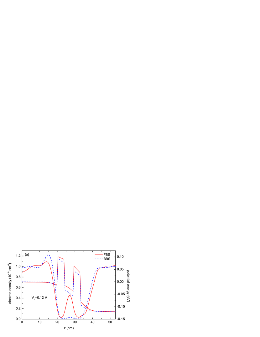
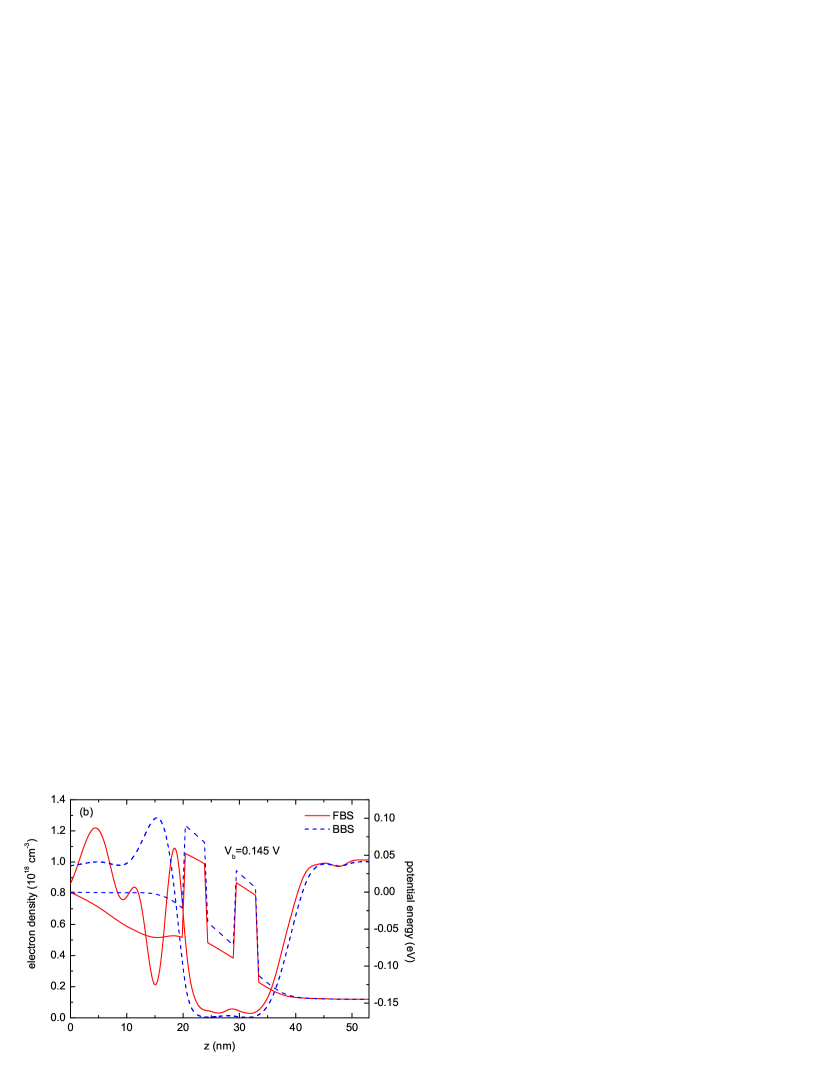
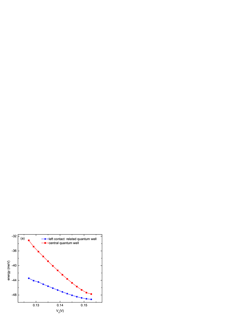
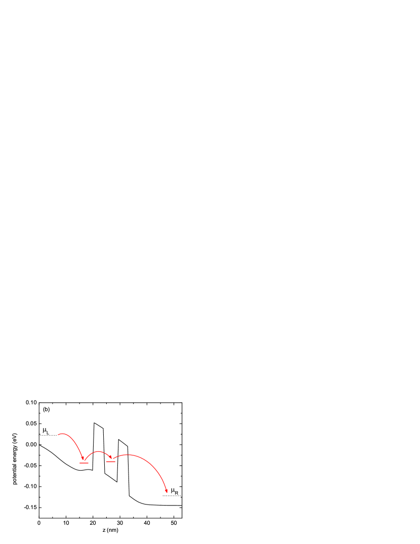
The current hysteresis in bias voltage range (II) located above the bias corresponding to the resonant current peak manifests itself as the increase of the current in the NDR region on the current-voltage characteristics [cf. Fig. 2]. In this range of bias voltage, the potential energy profiles and electron density distributions obtained for the increasing and decreasing bias voltage are different (Fig. 7(b)), they also exhibit an essential difference in comparison to those obtained for range (I) [cf. Fig. 7(a)]. In the case of FBS, we observe the depletion of the electron density in the region of the left contact and the formation of the shallow potential well in this region. In the NDR region the system rapidly escapes from the resonant tunneling condition and consequently the reflection probability from the left barrier drastically increases. The wave function of the electron incoming from the left reservoir interfere with the wave function of the electron reflected from the left barrier, which leads to the electron density oscillations in the region of the left contact [cf. Fig. 7(b)]. In a self-consistent manner, this electron density distribution leads to creation of the shallow potential well, in which the quasi-bound state can be formed. The results of calculations of the energy expectation values for the quasi-bound states in the central quantum well and in the quantum well located in the left contact [Fig. 8(a)] allow to explain the relation between these quasi-bound states. It appears that for each bias voltage value from region (II) the energy of the quasi-bound state localized in the region of the left contact is lower than the energy of the quasi-bound state localized in the central quantum well. If the bias voltage increases, the difference between these energies decreases from meV for V to meV for V. We note that this energy difference is small and comparable to the energy broadening of the corresponding energy level. Therefore, the resonant tunneling conditions are satisfied for some range of the bias voltage and the electrons can tunnel via the quasi-bound states from the left contact through the central quantum well to the right contact leading to the linear increase of the current in the NDR region. The resonant tunneling that occurs for the FBS in region (II) is schematically illustrated in Fig. 8(b). In the case of BBS, the potential well in the left contact region is not deep enough in order to the quasi-bound state to be formed [cf. Fig. 7(b)]. Therefore, the tunneling can appear with a very small probability and the BBS current is very small. These effects lead to the current hysteresis in bias voltage range (II) located above the resonant current peak.
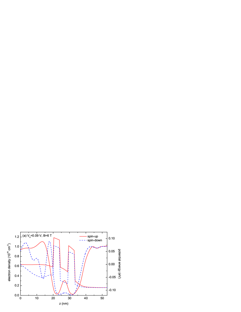
The plateau behavior of the spin current polarization that appears in certain ranges of the bias voltage (Fig. 5) and magnetic field (Fig. 6) are the most interesting results of the present calculations. We demonstrate that all of these plateaus are caused by the tunneling of spin-polarized electrons through the quasi-bound state in the region of the left contact. As we mentioned before the same process leads to the increase of the current in the NDR region and consequently the current hysteresis occurring in bias voltage range (II). For this purpose we analyze the spin-dependent electron distributions and potential energy profiles calculated for different bias voltage values at the fixed magnetic field (Fig. 9) and for different values of the magnetic fields at the fixed bias voltage (Fig. 10). Fig. 9 displays the results for the two bias voltage values that correspond to the two plateaus of spin current polarization in the lower and higher bias voltage regions (cf. Fig. 5). Fig. 9(a) shows that – for the lower bias voltage and for the spin-down electrons – we deal with the charge depletion in the central quantum well and the formation of the quantum well in the region of the left contact. In this quantum well, the spin-down electrons can be accumulated in the weakly bound states. In the higher bias voltage region [Fig. 9(b)], the roles of electron spin states are interchanged. As a result, the charge depletion appears for the spin-up states in the central quantum well and the spin-up electrons become accumulated in the left-contact related potential well. Therefore, in both the lower and higher bias voltage regions, the almost constant spin current polarization results from the resonant tunneling of the spin-polarized electrons via the quasi-bound state formed in the region of the left contact. The current of the spin-down electrons is responsible for the plateau in the lower bias voltage range, while the plateau of the spin current polarization in the higher bias voltage range is due to the resonant tunneling of the spin-up electrons.

The spin current polarization versus magnetic field dependence exhibits three plateaus for the bias voltage V (cf. Fig. 6). In order to explain the origin of this interesting behavior we have calculated the spin-dependent electron distributions and potential energy profiles for magnetic fields =1 T, 2 T, and 4 T that correspond to the first, second, and third plateau, respectively, on the curve (Fig. 10). In the magnetic field range corresponding to the first plateau (Fig. 10(a)), we have obtained the depletion of both the spin-up and spin-down electrons in the central quantum-well region. Moreover, in the region of the left contact, the shallow quantum well is formed for both the spin-up and spin-down electrons. In this left-contact related potential well, the quasi-bound states of the electrons with either spin can be created. These quasi-bound states participate in the resonant tunneling through the paramagnetic RTD by means of the same process as observed in case of the electron tunneling in the range of the current hysteresis marked (II) on Fig. 2(c).
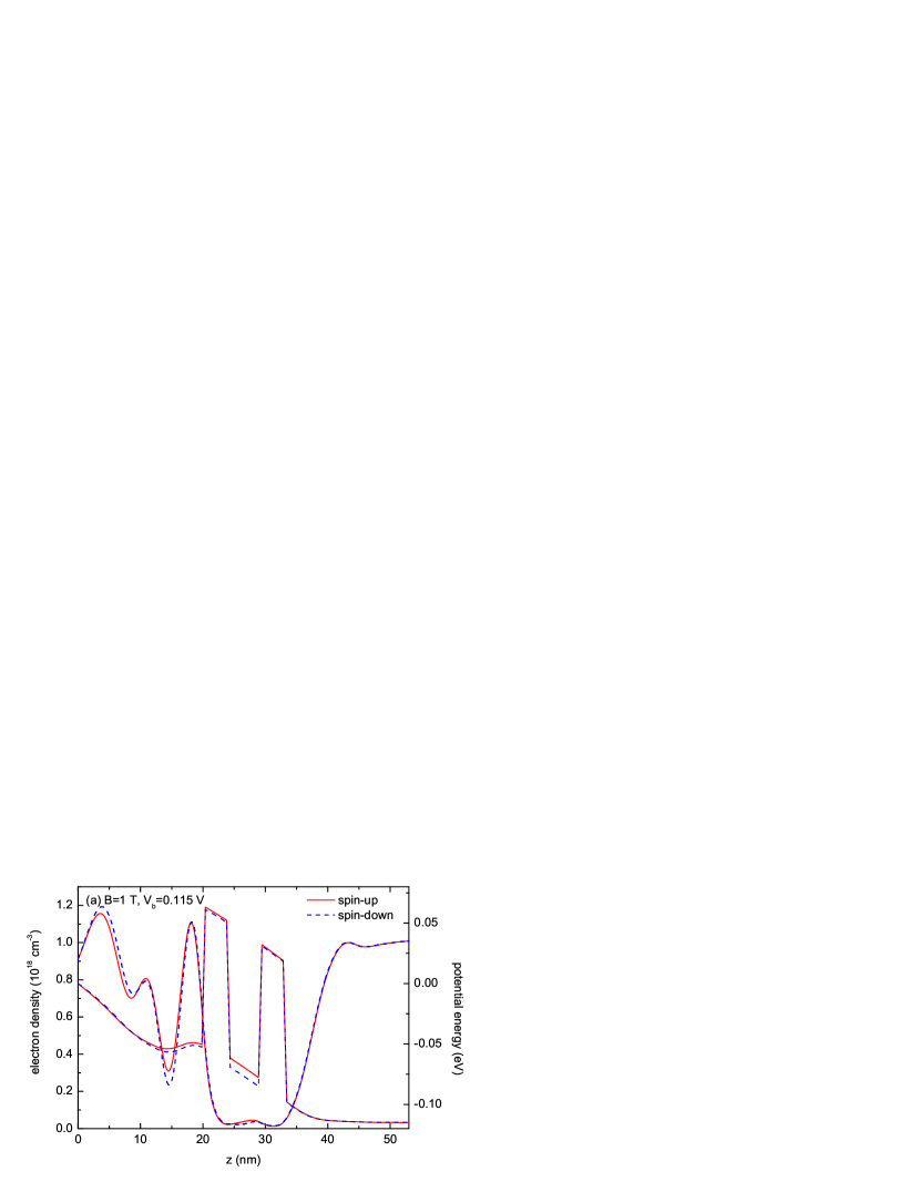
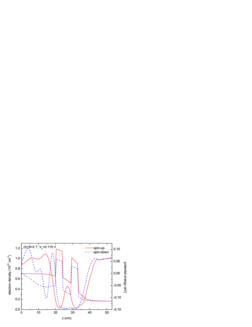
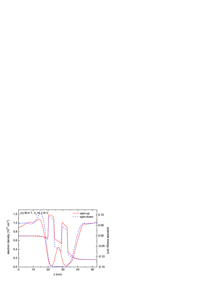
Since the potential energy profiles and electron densities for the spin-up and spin-down electrons are nearly the same, both the spin currents are almost equal to each other, which leads to the vanishing spin current polarization [cf. Fig. 10(a)]. The increasing magnetic field changes – in different manner – the resonant tunneling conditions for each spin polarization of the current. If magnetic field exceeds T, the quantum well for spin-up electrons in the region of the left contact disappears [Fig. 10(b)]. At high magnetic fields, the spin-up electrons become accumulated in the central quantum-well layer. This means that in the region of the central quantum well the resonant tunneling condition is satisfied only for the spin-up electrons, whereas the spin-down electrons can tunnel through the quasi-bound state in the region of left contact. Therefore, the spin-up current component becomes large, while the spin-down component is only slightly changed (cf. Fig. 2). As a result of these changes, we obtain – at the intermediate magnetic field (Fig. 6) – the second plateau of the spin current polarization with . If the magnetic field exceeds T, the left-contact related quantum well also disappears for the spin-down electrons. At high magnetic fields, the density of the spin-up (spin-down) electrons is large (small) in the central quantum well. In this case, the resonant tunneling condition is satisfied for the spin-up electrons, while the spin-down electrons are out of the resonance. Therefore, the spin-up current reaches the maximum while the spin-down current becomes negligibly small [cf. Fig. 2(d)]. This leads to the third plateau on the curve with , i.e., we obtain the almost full spin current polarization in the high magnetic field ranges (Fig. 6). We note that for the lower and higher bias voltage the system makes the direct transition to the fully polarized spin current at certain magnetic field (cf. Fig. 6).
V Conclusions and Summary
In the present paper, we have studied the spin-dependent electron transport through the paramagnetic RTD based on Zn1-xMnxSe/Zn0.95Be0.05Se heterostructure. The current-voltage characteristics of the nanodevice have been determined by the numerical solution of self-consistent Wigner-Poisson model of electron transport in the framework of the two-current model. The application of the two-current model is fully justified in the case of the nanodevice because the magnetic field produces the giant Zeeman splitting [Eq. (1)] which modifies the potential energy profile and as a result the electrons with opposite spins independently tunnel via the different quantum-well states. Numerical estimation of the ratio of the cyclotron resonance energy , where , to the Fermi energy of -doped ZnSe for maximum value of magnetic field ( = 8 T) which is considered in this paper gives 0.46. It means that the relative strength of the maximum magnetic field is rather weak and therefore we can neglect the effect of magnetic field quantization. Due to the complexity of the numerical calculations, we have neglected the intervalley coupling and effects of the electron scattering processes which result from the interaction of electrons with phonons and impurities.
The calculated current-voltage characteristics exhibit two separated resonant current peaks that correspond to the spin-up and spin-down current components. We have found that the current hysteresis appears on the current-voltage characteristics for each spin polarization of the current. The current hysteresis occurs in two distinct bias voltage regions: the first with the bias voltage values below that corresponding to the resonant current peak and the second – above the resonant current peak. The analysis of the self-consistent potential energy profiles and electron density distributions in the nanodevice allows us to give the physical interpretation of these effects. We have demonstrated that the current hysteresis in the first bias voltage region is related to the charge accumulation in the central quantum-well layer, while the current hysteresis in the second bias voltage region results from the resonant tunneling through the quasi-bound state created in the region of the left contact. We have shown that the current hysteresis leads to the different spin polarization for the forward and backward bias sweeps, which – in turn – leads to the appearance of the plateaus that appear on the spin current polarization dependence on the bias voltage and magnetic field. For certain plateaus the current is almost fully spin-polarized. We have determined the conditions for the full spin current polarization and discussed the underlying physics. This property is very promising for future spintronic devices.
We expect that including the scattering of electrons should result in more smooth current-voltage characteristics and the decrease of the spin current polarization. Moreover, the exchange interaction between the conduction-band electrons has been neglected in the present calculations. We have also performed the calculations with the exchange interaction taken into account by the local density approximation. The preliminary results show that the incorporation of the interelectron exchange changes the present results only slightly, in particular, the maximum current polarization becomes slightly smaller and the rapid changes on the current-voltage characteristics become more smooth. We conclude that the exchange interaction between the conduction-band electrons has no significant influence on the present results.
In summary, we have shown that the electron current flowing through the non-magneticmagneticnon-magnetic double barrier heterostructure (paramagnetic RTD) can exhibit the hysteresis that appears on the current-voltage characteristics for the spin-polarized current. Moreover, we have determined the regions of the bias voltage and ranges of magnetic field, in which the pronounced spin current polarization occurs in the paramagnetic RTD. The results of the present paper allow us to predict the conditions, under which we obtain the spin-polarized current in the double-barrier heterostructure with the manganese doped quantum-well layer.
Acknowledgements.
This paper has been supported by the Foundation for Polish Science MPD Programme co-financed by the EU European Regional Development Fund and by the AGH-University of Science and Technology under project no. 11.11.220.01 ”Basic and applied research in nuclear and solid state physics”.References
- (1) H. Ohno, H. Munekata, T. Penney, S. von Molnár, and L. L. Chang, Phys. Rev. Lett. 68, 2664 (1992)
- (2) H. Ohno, Science 281, 951 (1998)
- (3) T. Hayashi, Y. Hashimoto, S. Katsumoto, and Y. Iye, Appl. Phys. Lett. 78, 1691 (2001)
- (4) K. W. Edmonds, K. Y. Wang, R. P. Campion, A. C. Neumann, N. R. S. Farley, B. L. Gallagher, and C. T. Foxon, Appl. Phys. Lett. 81, 4991 (2002)
- (5) K. M. Yu, W. Walukiewicz, T. Wojtowicz, I. Kuryliszyn, X. Liu, Y. Sasaki, and J. K. Furdyna, Phys. Rev. B 65, 201303 (2002)
- (6) D. Chiba, K. Takamura, F. Matsukura, and H. Ohno, Appl. Phys. Lett. 82, 3020 (2003)
- (7) K. C. Ku, S. J. Potashnik, R. F. Wang, S. H. Chun, P. Schiffer, N. Samarth, S. M. J, A. Mascarenhas, E. Johnston-Halperin, R. C. Myers, A. C. Gossard, and D. D. Awschalom, Appl. Phys. Lett. 82, 2302 (2003)
- (8) K. F. Eid, B. L. Sheu, O. Maksimov, M. B. Stone, P. Schiffer, and N. Samarth, Appl. Phys. Lett. 86, 152505 (2005)
- (9) T. Jungwirth, K. Y. Wang, J. Masek, K. W. Edmonds, J. König, J. Sinova, M. Polini, N. A. Goncharuk, A. H. MacDonald, M. Sawicki, R. P. Campion, L. X. Zhao, C. T. Foxon, and B. L. Gallagher, Phys. Rev. B 72, 165204 (2005)
- (10) J. K. Furdyna, J. Appl. Phys. 64, R29 (1988)
- (11) W. Y. Yu, A. Twardowski, L. P. Fu, and A. Petrou, Phys. Rev. B 51, 9722 (1995)
- (12) K. Ando, Appl. Phys. Lett. 82, 100 (2003)
- (13) C. Liu, F. Yun, and H. Morkor, J. Mater. Sci.: Mater. Electron. 16, 555 (2005)
- (14) T. Jungwirth, J. Sinova, J. Masek, J. Kucera, and A. H. MacDonald, Rev. Mod. Phys. 78, 809 (2006)
- (15) T. Dietl, H. Ohno, and F. Matsukura, Phys. Rev. B 63, 195205 (2001)
- (16) T. Gruber, M. Keim, R. Fiederling, G. Reuscher, W. Ossau, G. Schmidt, L. W. Molenkamp, and A. Waag, Appl. Phys. Lett. 78, 1101 (2001)
- (17) A. Slobodskyy, C. Gould, T. Slobodskyy, C. R. Becker, G. Schmidt, and L. W. Molenkamp, Phys. Rev. Lett. 90, 246601 (2003)
- (18) N. N. Beletskii, G. P. Berman, and S. A. Borysenko, Phys. Rev. B 71, 125325 (2003)
- (19) S. Datta and B. Das, Appl. Phys. Lett. 56, 665 (1990)
- (20) J. C. Egues, Phys. Rev. Lett. 80, 4578 (1998)
- (21) P. Havu, N. Tuomisto, R. Väänäne, M. J. Puska, and R. M. Nieminen, Phys. Rev. B 71, 235301 (2005)
- (22) V. J. Goldman, D. C. Tsui, and J. E. Cunningham, Phys. Rev. Lett. 58, 1256 (1987)
- (23) F. W. Sheard and G. A. Toombs, Appl. Phys. Lett. 52, 1228 (1988)
- (24) T. C. L. G. Sollner, Phys. Rev. Lett. 59, 1622 (1987)
- (25) B. Su, V. J. Goldman, M. Santos, and M. Shayegan, Appl. Phys. Lett. 58, 747 (1991)
- (26) L. D. Macks, S. A. Brown, R. G. Clark, R. P. Starrett, M. A. Reed, M. R. Deshpande, C. J. L. Fernando, and W. R. Frensley, Phys. Rev. B 54, 4857 (1996)
- (27) V. J. Goldman, D. C. Tsui, and J. E. Cunningham, Phys. Rev. B 36, 7635 (1987)
- (28) Z. Dai and J. Ni, Phys. Rev. B 73, 113309 (2006)
- (29) A. Twardowski, M. von Ortenberg, M. Demianiuk, and R. Pauthenet, Solid State Commun. 51, 849 (1984)
- (30) P. Wójcik, B. J. Spisak, M. Wołoszyn, and J. Adamowski, Semicond. Sci. Technol. 25, 125012 (2010)
- (31) J. M. Ziman, Electrons and phonons: the theory of transport phenomena in solids (Oxford University Press, 2000)
- (32) B. J. Spisak, M. Wołoszyn, P. Wójcik, and G. J. Morgan, J. Phys.: Conf. Ser. 193, 012130 (2009)
- (33) M. Q. Weng and M. W. We, J. Appl. Phys. 93, 410 (2003)
- (34) B. J. Spisak, A. Paja, and G. J. Morgan, phys. stat. sol. (b) 242, 1460 (2005)
- (35) K. Y. Kim, J. Appl. Phys. 102, 113705 (2007)
- (36) W. R. Frensley, Rev. Mod. Phys. 62, 745 (1990)
- (37) D. K. Ferry, S. M. Goodnick, and J. P. Bird, Transport in nanostructures (Cambridge University Press, 2009)
- (38) C. Chauvet, E. Tournié, and J. P. Faurie, Phys. Rev. B 61, 5332 (2000)