Switching dynamics of a magnetostrictive single-domain nanomagnet subjected to stress
Abstract
The temporal evolution of the magnetization vector of a single-domain magnetostrictive nanomagnet, subjected to in-plane stress, is studied by solving the Landau-Lifshitz-Gilbert equation. The stress is ramped up linearly in time and the switching delay, which is the time it takes for the magnetization to flip, is computed as a function of the ramp rate. For high levels of stress, the delay exhibits a non-monotonic dependence on the ramp rate, indicating that there is an optimum ramp rate to achieve the shortest delay. For constant ramp rate, the delay initially decreases with increasing stress but then saturates showing that the trade-off between the delay and the stress (or the energy dissipated in switching) becomes less and less favorable with increasing stress. All of these features are due to a complex interplay between the in-plane and out-of-plane dynamics of the magnetization vector induced by stress.
pacs:
85.75.Ff, 75.85.+t, 75.78.Fg, 85.40.BhI Introduction
There is significant interest in studying the magnetization reversal dynamics of multiferroic (strain-coupled magnetostrictive/piezoelectric bilayer) nanomagnets subjected to stress. This has potential applications in ultralow power non-volatile magnetic logic and memory Roy et al. ; D’Souza et al. ; Atulasimha and Bandyopadhyay (2010); Fashami et al. ; Brintlinger et al. (2010); Wolf et al. (2010); Zavaliche et al. (2007) because switching a multiferroic nanomagnet with stress dissipates far less energy than switching it with a magnetic field or spin transfer torque produced by a current Roy et al. . As a result, stress-mediated switching can reduce energy dissipation in magnetic reversal to the point where non-volatile memory and logic systems can be run by harvesting energy solely from the environment without needing a power source or battery! This opens up unique applications in situations where energy is a premium – such as in implanted medical devices, structural health monitoring systems, “wearable” electronics, and space based applications.
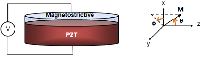
A multiferroic nanomagnet is made of a magnetostrictive layer and a piezoelectric layer in intimate contact with each other (see Figure 1). A voltage applied across the piezoelectric layer generates in it a mechanical strain that is mostly transferred to the magnetostrictive layer by elastic coupling and produces an extension Eerenstein et al. (2006); Nan et al. (2008) if the latter layer is much thinner than the former. If we mechanically constrain the magnetostrictive layer from expanding or contracting along a certain in-plane direction, e.g. along the minor axis of the ellipse in Figure 1, then this will generate uniaxial stress along the major axis through the coupling in the piezoelectric. This stress will cause the magnetization axis of the magnetostrictive layer (nanomagnet) to rotate by a large angle Atulasimha et al. (2008), which has been demonstrated in recent experiments Brintlinger et al. (2010), although not in nanoscale.
Let us assume that the shape of the nanomagnet is that of an elliptical cylinder as shown in Figure 1 and that the initial orientation of the magnetization is close to the major axis of the ellipse (z-axis), which is the magnet’s easy axis. In that case, a 90∘ rotation will place the magnetization vector along the minor axis, which is the in-plane hard axis. Subsequent removal of stress can relax it back to the easy axis, but in a direction anti-parallel to the initial direction, resulting in a 180∘ rotation or “flip” Roy et al. . Ref. [Roy et al., ] showed that the energy dissipated in this process is extremely small (200 at room temperature) for optimum choice of materials, even when the switching takes place in 1 nanosecond and the stress is turned on abruptly and instantaneously. In fact, a tiny voltage of few mV applied abruptly can generate enough stress to flip the magnetization Roy et al. ; Atulasimha and Bandyopadhyay (2010) in 1 nanosecond, which results in the miniscule dissipation of 200 .
In this paper, we are concerned with the following issue. The applied voltage cannot generate strain in the magnetostrictive layer instantaneously. If we ramp up the voltage gradually with a rise time longer than the response time of strain, then strain may be able to follow the voltage quasi-statically. In that case, by controlling the ramp rate of the voltage, we can control the rise time of the strain. This may have significant effects on both the switching delay and the energy dissipated in the switching process. The purpose of this paper is to investigate this possibility.
Intuitively, one would expect that if the stress is always ramped up to a constant value regardless of the ramp rate, then the time taken to flip the magnetization (switching delay), will decrease monotonically with increasing ramp rate. The only caveat is that at high stress levels, a very fast ramp rate may cause ripples and ringing in the temporal evolution of the magnetization vector, which may prolong the switching process. The actual situation turns out to be a little more complicated because the switching dynamics exhibits rich and complex behavior as a result of the interplay between the in-plane and out-of-plane excursions of the magnetization vector under application of stress. This complex interplay has two effects: (1) it makes the switching delay exhibit a non-monotonic dependence on the ramp rate when high stresses are encountered, and (2) it makes the switching delay saturate quickly with increasing stress at a constant ramp rate. In this paper, we have studied this intriguing dynamics by solving the Landau-Lifshitz-Gilbert (LLG) equation which governs the temporal evolution of the magnetization vector of a single domain nanomagnet.
The rest of this paper is organized as follows. In Section II, we first derive the torque exerted by any applied stress on the magnetization vector of the magnetostrictive layer, and then solve the LLG equation analytically in the spherical coordinate system to yield equations that govern the time evolution of the magnetization vector. These equations describe how the polar angle and the azimuthal angle of the magnetization vector change with time. They are solved numerically to obtain the dynamics of magnetization rotation. In Section III, we derive the energy landscapes of the nanomagnet (energy as a function of magnetization orientation) in the stressed and relaxed conditions since they are a valuable aid in understanding the time evolution of the magnetization vector. In Section IV, we present the simulation results, while in Section V we discuss the implications of these results and present the conclusions.
II Solution of the Landau-Lifshitz-Gilbert equation
Consider an isolated nanomagnet in the shape of an elliptical cylinder whose elliptical cross section lies in the y-z plane with its major axis aligned along the z-direction and minor axis along the y-direction. The dimension of the major axis is , that of the minor axis is , and the thickness is . The volume of the nanomagnet is . Let be the angle subtended by the magnetization axis with the +z-axis at any instant of time and be the angle between the +x-axis and the projection of the magnetization axis on the x-y plane. Thus, is the polar angle and is the azimuthal angle. Note that when = 90∘, the magnetization vector lies in the plane of the magnet. Any deviation from = 90∘ corresponds to out-of-plane motion.
The total energy of the single-domain nanomagnet (magnetostrictive layer) is the sum of the uniaxial shape anisotropy energy and the uniaxial stress anisotropy energy:
| (1) |
where is the uniaxial shape anisotropy energy and is the uniaxial stress anisotropy energy at time . The former is given by
| (2) |
where is the saturation magnetization and is the demagnetization factor expressed as Chikazumi (1964)
| (3) |
with , , and are the components of the demagnetization factor along the -axis, -axis, and -axis, respectively. When and are nearly equal, and , , , and are approximately given by Chikazumi (1964)
| (4a) | ||||
| (4b) | ||||
| (4c) | ||||
More accurate expressions for these quantities can be found in Ref. [Beleggia et al., 2005].
Note that uniaxial shape anisotropy will favor lining up the magnetization along the major axis (-axis) by minimizing , which is why we will call the major axis the “easy axis” and the minor axis (y-axis) the “hard axis” in the plane of the magnet. By mechanically constraining the nanomagnet from expanding or contracting in the y-direction using appropriate clamps, we will generate uniaxial stress along the -axis (easy axis). In that case, the stress anisotropy energy is given by
| (5) |
where is the magnetostriction coefficient of the nanomagnet and is the stress generated in it by an external agent. Note that a positive product will favor alignment of the magnetization along the major axis (-axis), while a negative product will favor alignment along the minor axis (-axis), because that will minimize . In our convention, a compressive stress is negative and tensile stress is positive. Therefore, in a material like Terfenol-D that has positive , a compressive stress will favor alignment along the minor axis, and tensile along the major axis. The situation will be opposite with nickel and coblat that have negative .
At any instant of time, the total energy of the nanomagnet can be expressed as
| (6) |
where
| (7a) | ||||
| (7b) | ||||
| (7c) | ||||
| (7d) | ||||
Note that is always positive for our choice of geometry, but can be negative or positive in accordance with the sign of the product.
The magnetization M(t) of the nanomagnet has a constant magnitude at any given temperature but a variable direction, so that we can represent it by the vector of unit norm where is the unit vector in the radial direction in spherical coordinate system represented by (,,). The other two unit vectors in the spherical coordinate system are denoted by and for and rotations, respectively. The gradient of potential energy at any particular instant of time is given by
| (8) |
where
| (9) | |||||
| (10) | |||||
while
| (11) |
The torque acting on the magnetization per unit volume due to shape and stress anisotropy is
| (12) | |||||
This torque causes the magnetization vector to rotate. The magnetization dynamics under the action of this torque is described by the Landau-Lifshitz-Gilbert (LLG) equation as follows.
| (13) |
where is the dimensionless phenomenological Gilbert damping constant, is the gyromagnetic ratio for electrons and is equal to (rad.m).(A.s)-1, is the Bohr magneton, and . In the spherical coordinate system,
| (14) |
Accordingly,
| (15) |
where ()’ denotes . This allows us to write
| (16) |
Equating the and components in both sides of Equation (13), we get
| (17) |
| (18) |
Solving the above equations, we get the following coupled equations for the dynamics of and .
| (20) |
We should note that the Equations (12), (II), and (20) are not valid when ( or ), i.e. when the magnetization direction is exactly along the easy axis. At these points, the torque on the magnetization vector given by Equation (12) diverges. In order to avoid these points, we will assume that the initial orientation of the magnet is , and switching is deemed to have been completed when . This 1∘ deflection could be caused by thermal fluctuations. Similar assumptions have been made by other authors Nikonov et al. (2010).
Equation (12) shows that there is an internal feedback in the system. Stress induces a torque which produces the rotation (, ). That rotation generates an additional torque through the and terms. That additional torque affects the response. This feedback mechanism determines the relation between the rotation and stress, and hence the switching delay as a function of stress.
Note from Equation (12) that the torque has contributions due to the dynamic change in stress (, terms). These contributions may aid or hinder the rotation of the magnetization vector at different times. This is why the switching delay will depend on the ramp rate . This dependence turns out to be non-monotonic because of the complex actions of the magnetization vector.
Note from Equation (11) that the term will be negative when . In that case, its contribution to the time rate of change of , i.e. , will be positive, as we can see from Equation (II). In other words, a negative will tend to increase with time. Since our initial value of is 179∘ and the final value is 1∘, we would prefer that will always decrease – and never increase – with time in order to complete the switching in the shortest time. Therefore, a negative value of , or equivalently lying in the interval [], is counterproductive since that makes increase with time, causing the magnetization to rotate in the wrong direction, opposite to the preferred direction. This hinders switching and increases the switching delay. Therefore, we will always prefer that remains positive, or equivalently remains in the interval [0∘, 90∘] or [180∘, 270∘].
On the other hand, it is clear from Equation (20) that a positive makes a positive contribution to the rate , which will tend to increase with time and make it exceed 90∘. These two counteracting influences of determine the actual switching dynamics and the resulting switching delay.
Another point to note is that when the applied stress is sufficiently high, the stress term dominates the term in Equations (II) and (20). The term involving should remain positivein Equation (II) in order to help remain negative so that the magnetization vector can rotate in the right direction. In order to keep negative, we will have to ensure that the product is negative. For materials with positive magnetostriction (e.g. Terfenol-D), this requires that the stress is negative, while for materials with negative magnetostriction (e.g. nickel or cobalt), the stress should be positive. Since tensile stress is positive and compressive is negative, Terfenol-D will require compressive stress and nickel or cobalt will require tensile stress to initiate switching if the magnetization is initially aligned close to the easy axis.
III Energy landscape
The energy landscape of a nanomagnet, which plots the total energy as a function of the polar angle and the azimuthal angle , provides valuable information. The final state of the magnetization will always be at an energy minimum. Stress will modify the energy landscape of a nanomagnet and shift the energy minimum from one set of angles to another , thereby effecting switching of the magnetization.
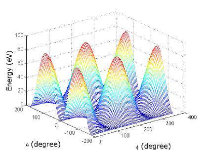
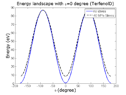
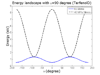
Figure 2 shows the energy landscape of a Terfenol-D/PZT multiferroic nanomagnet for and without any applied stress. Figures 3 and 3 show how stress modifies the energy landscape in -space for and , respectively.
When , i.e. the magnetization vector lies in the x-z plane, the energy barrier separating the two stable magnetizations along the z-axis (easy-axis) is 10 times taller than what it is when , i.e. when the magnetization vector lies in the y-z plane. This happens because the thickness of the nanomagnet is much smaller than the other two dimensions, which makes the shape anisotropy energy barrier much taller in the former case than in the latter case. The stress that can be generated in the magnetostrictive layer by the strained piezoelectric layer is usually sufficient to rotate the magnetization axis when , because the shape anisotropy barrier that has to be overcome is small. However, this does not necessarily happen when because then the shape anisotropy energy barrier is much higher. On the other hand, out-of-plane excursion of the magnetization vector generates an additional torque that aids switching. Thus, some out-of-plane excursion is beneficial, but if the magnetization vector strays out of plane, it encounters a larger energy barrier that prevents switching. Therefore, the magnetization vector must precess and ultimately return close to the nanomagnet’s plane before switching can be accomplished. This is the cause of precessional motion.
The energy landscapes allow us to estimate the minimum stress needed to rotate the magnetization vector from the initial orientation close to the easy axis to the in-plane hard axis. Once the vector aligns along the in-plane hard axis, stress is removed. Thereafter, the magnetization vector will relax back to the easy axis but to an orientation anti-parallel to the initial orientation. This results in switching. The minimum stress required for this purpose is found by equating the shape anisotropy energy barrier to the stress anisotropy energy, i.e.
| (21) |
which yields
| (22) |
However, switching with this minimum stress will incur a very long switching delay, so that some excess stress will be needed to switch the magnetization reasonably fast. Normally, one would expect the switching delay to decrease continuously with increasing excess stress, but in reality it saturates beyond a certain stress so that increasing stress further offers only marginal advantage. This feature cannot be understood from the energy landscape because it is a consequence of the interplay between the in-plane and out-of-plane dynamics of the magnetization vector, which is not captured in the energy profiles.
| Terfenol-D | Nickel | Cobalt | |
|---|---|---|---|
| Major axis (a) | 101.75 nm | 105 nm | 101.75 nm |
| Minor axis (b) | 98.25 nm | 95 nm | 98.25 nm |
| Thickness (t) | 10 nm | 10 nm | 10 nm |
| Young’s modulus (Y) | 81010 Pa | 2.141011 Pa | 2.091011 Pa |
| Magnetostrictive coefficient () | +9010-5 | -310-5 | -310-5 |
| Saturation magnetization () | 8105 A/m | 4.84105 A/m | 8105 A/m |
| Gilbert’s damping constant () | 0.1 | 0.045 | 0.01 |
IV Simulation results
We consider a multiferroic nanomagnet composed of a PZT layer (lead-zirconate-titanate) and a magnetostrictive layer which is made of either polycrystalline Terfenol-D, or polycrystalline nickel, or polycrystalline cobalt. Because it is polycrystalline, the magnetocrystalline layer does not have significant magnetocrystalline anisotropy. The material parameters for the magnetostrictive layer are given in Table 1 Abbundi and Clark (1977); Ried et al. (1998); Kellogg and Flatau (2008); Walowski et al. (2008); mat . They ensure that the shape anisotropy energy barrier is 32 kT at room temperature. The PZT layer is assumed to be four times thicker than the magnetostrictive layer so that any strain generated in it is transferred almost completely to the magnetostrictive layer. We will assume that the maximum strain that can be generated in the PZT layer is 500 ppm Lisca et al. (2006), which would require a voltage of 111 mV because =1.8e-10 m/V for PZT pzt . The corresponding stress is the product of the generated strain () and the Young’s modulus of the magnetostrictive layer. Based on available data for Young’s modulus, the maximum allowable stresses for Terfenol-D, nickel, and cobalt are 40 MPa, 107 MPa, and 104.5 MPa, respectively.
In all our simulations, the initial orientation of the magnetization vector is: and . Stress is applied as a linear ramp and we solve Equations (II) and (20) at each time step. Once becomes 90∘, stress is removed and we follow the magnetization vector in time until becomes 1∘. At that point, switching is deemed to have occurred.
We assume that the voltage applied on the piezoelectric is ramped up linearly to its steady-state value in time which we call the rise time. When the stress is ramped down, we use the same rate, i.e. we reduce the stress from its maximum value to zero in time . In all cases, the rise time is equal to the fall time.
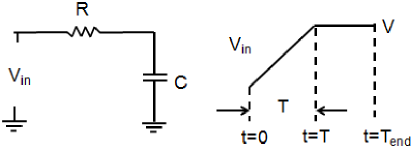
We also assume that the PZT layer, which acts as a capacitor, is electrically accessed with a silver wire of resistivity 2.6 -cm int so that a typical access line of length 10 and cross section 50 nm 50 nm will have a resistance of 100 . Based on the dimensions of the PZT layer (major axis, minor axis, and thickness), and assuming that the relative dielectric constant of PZT is 1000, the capacitance of the PZT layer will be 2 fF. Therefore, the RC time constant associated with charging the capacitor is 0.2 ps. Since the range of ramp time considered in our simulation is 1-150 ps, we are in the adiabatic limit () and hence the energy dissipation in the external circuit that generates the voltage across the PZT layer will be less than (1/2). We assume that the charging circuit is represented by the circuit diagram in Figure 4. The energy dissipated during the rise of the voltage (charging cycle) for a signal of total time-period and ramp-period can be calculated as below.
| (23) |
where is the capacitance of the PZT layer and is the steady state voltage that generates the required stress. The last term in the above expression comes from a finite value of .
The energy dissipated during the discharging cycle is , which can be calculated from an expression similar to the one above, except that the value of may be different. For the sake of brevity, we will term the total energy dissipated in the charging circuit as the ‘’ energy dissipation in the remainder of this paper.
Because of Gilbert damping in the magnet, an additional energy is dissipated when the nanomagnet switches. This energy is given by the expression
| (24) |
where is the switching delay and , which is the dissipated power, is given by Sun and Wang (2005); Behin-Aein et al. (2009)
| (25) |
We sum up the power numerically throughout the switching period to get the corresponding energy dissipation and add that to the ‘’ dissipation in the switching circuit to find the total dissipation . The average power dissipated during switching is simply .
We analyze the magnetization dynamics of the magnetostrictive layer as a function of both the magnitude and the ramp time of the stress for three different materials (Terfenol-D, nickel, cobalt). The results are presented in the ensuing subsections. These materials are chosen because of their very different material parameters such as Gilbert damping constant, saturation magnetization, and magnetostrictive coefficient.
IV.1 Terfenol-D
Terfenol-D has a positive magnetostrictive coefficient (see Table 1). Therefore, we will need a compressive stress to rotate the magnetization vector away from its initial alignment close to easy axis ( = 179∘) towards = 90∘. Note that we need to use the correct voltage polarity to ensure that a compressive stress is generated on the Terfenol-D layer. The maximum stress that can be generated on the Terfenol-D layer with the maximum allowed 500 ppm strain in the PZT layer is 40 MPa, and the minimum stress that is needed to switch the nanomagnet is found by equating the stress anisotropy energy to the shape anisotropy energy barrier. This stress is 1.91 MPa.
IV.1.1 Ramp rate and switching delay
Equations (II) and (20), derived in Section II, are solved numerically to find the values of and at any given instant . This yields the magnetization dynamics under various stresses and ramp rates.
Fast ramp:
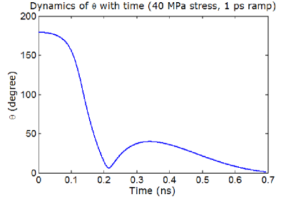
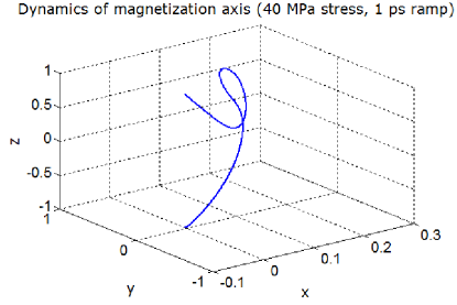
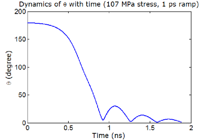
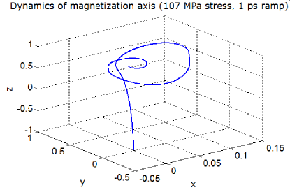
The stress on the Terfenol-D layer is ramped up linearly in time from 0 to the maximum possible value of 40 MPa in 1 ps. The corresponding magnetization dynamics is shown in Figure 5. We notice that the polar angle continuously evolves from its initial value of 179∘ towards its final value of 1∘ for the first 200 ps. However, because of the coupled dynamics of the azimuthal angle and the polar angle , deviates from its initial value of 90∘ at around 200 ps, forcing the magnetization vector to venture out of plane. This makes the magnetization vector execute precessional motion in space while its projection on the magnet’s plane changes course and rotates in the direction opposite to the desired direction so that begins to increase with time instead of decreasing. Eventually, as the magnetization vector stops precessing and returns to the magnet’s plane, which happens around 330 ps, its projection on the magnet’s plane starts rotating towards its final destination, ultimately reaching = 1∘ and = 90∘. Because of the interplay between the - and -dynamics, which causes the magnetization vector to leave the plane of the nanomagnet after 200 ps, switching takes around 700 ps.
Slow ramp:
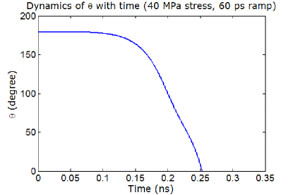
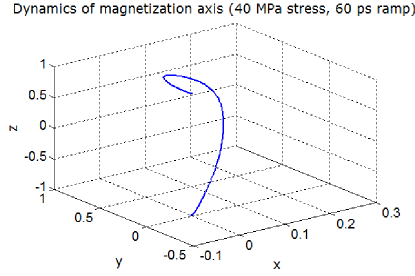
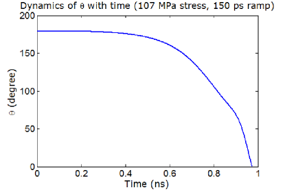
Figure 6 shows the magnetization dynamics for a slow ramp that takes 60 ps to rise linearly from 0 to 40 MPa. In this case, the magnetization vector does not even budge from its initial orientation of = 179∘ until the stress reaches its peak value of 40 MPa, which happens after 60 ps have elapsed. Thereafter, the magnetization vector rotates towards its final destination of = 1∘ without ever changing course and rotating in the opposite direction, unlike the previous case. The magnetization vector however does leave the magnet’s plane in this case as well, but clearly it does not precess as much as in the previous case (see the trajectory plot). The switching is actually faster now and takes only 250 ps compared to 700 ps for the previous case. Thus, a slower ramp can be beneficial when high stresses are applied. It eliminates the ripple and ringing in the switching characteristic seen in the previous case by limiting the out-of-plane excursion of the magnetization vector and saves precious time.
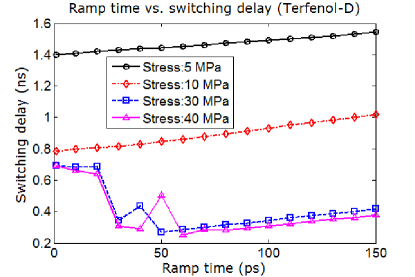
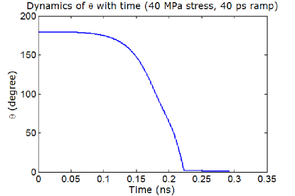
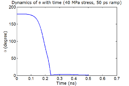
Figure 7 shows the switching delay as a function of the ramp’s rise (or fall) time with the magnitude of stress as a parameter. We see that for stresses of 5 MPa and 10 MPa, the switching delay increases linearly with the ramp time, but for higher stresses of 30 MPa and 40 MPa, the switching delay shows clear non-monotonic behavior for rise (and fall) times less than 60 ps. Normally, the switching delay should increase continuously with the ramp’s rise (and fall) time, but the out-of-plane dynamics and precession of the magnetization vector that occurs at very fast ramp rates can reverse this trend and cause the non-monotonic behavior. Figures 8 and 9 show the magnetization dynamics for ramp rise (and fall) times of 40 ps and 50 ps, respectively. There are some ripples in these cases also, but their amplitudes are much reduced so that they are barely visible in the plots. For ramp rise times exceeding 60 ps, the ripples disappear. Thereafter, the switching delay increases monotonically with the rise (or fall) time.
IV.1.2 Switching delay and energy dissipation
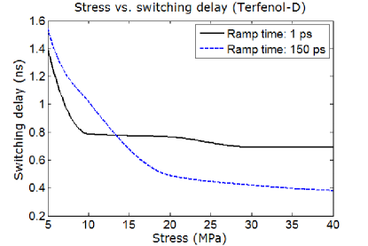
Figure 10 shows the dependence of the switching delay on stress in the Terfenol-D/PZT nanomagnet, with the ramp’s rise (or fall) time as a parameter. The two rise (and fall) times considered are 1 ps and 150 ps. There is a cross over at 14 MPa stress. At low stress levels below 14 MPa, not much ripple is generated by a fast ramp so that the switching delay is shorter for the faster ramp. At high stress levels exceeding 14 MPa, a fast ramp generates enough ripple that the switching delay becomes longer for the faster ramp. This is the reason for the cross over.
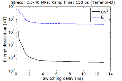
Figure 11 shows the energy dissipated in flipping the magnetization of the Terfenol-D/PZT multiferroic nanomagnet as a function of switching delay for a fixed rise (and fall) time of 150 ps. The switching delay is varied by varying the stress on the nanomagnet between 2.5 and 40 MPa. The energy dissipated internally in the nanomagnet () and the energy dissipated in the switching circuit (‘’) are shown separately. They both tend to saturate at larger delays.
For longer switching delays, the stress needed to flip the magnetization is less and hence the voltage needed to generate the stress is smaller. This leads to a smaller ‘’ dissipation in the switching circuit. At the same time, the energy dissipated internally in the nanomagnet is smaller when we switch slowly. In this range of switching delay, the energy dissipated in the external circuit is much smaller than the energy dissipated internally in the nanomagnet since the switching is adiabatic (the rise (and fall) time is much longer than the RC time constant of the switching circuit). The ratios of the two energies however decreases with decreasing switching delay. Below a switching delay of 4 ns, the energy dissipated internally in the nanomagnet and energy dissipated in the switching circuit both increase super-exponentially with decreasing switching delay. At 1 ns switching delay, the total energy dissipated in switching is only about 200 kT, which makes this switching methodology extremely energy-efficient. For this switching delay, the energy dissipated to switch a state-of-the-art transistor would have been at least two orders of magnitude larger itr , and the energy dissipated to switch the same nanomagnet with spin transfer torque will be also at least two orders of magnitude larger Fukami et al. (2009).
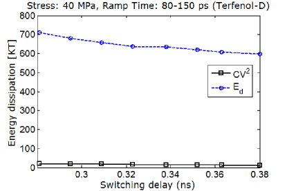
Figure 12 plots the energy dissipation as a function of switching delay for a fixed stress of 40 MPa. Here, the switching delay is varied by varying the ramp’s rise (and fall) time between 80 and 150 ps. A lower rise (or fall) time is avoided because of the non-monotonic behavior observed in Figure 7. Both and the ‘’ dissipations fall off with increasing switching delay. This means that the average power dissipation falls off even more rapidly with increasing switching delay since the energy dissipation is the product of the average power dissipation and the switching delay. This figure shows that we can switch in 0.3 - 0.4 ns by dissipating 600 - 700 kT of energy at room temperature.
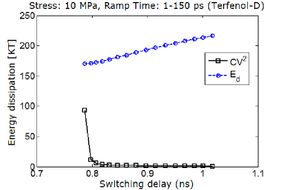
A similar plot for a lower fixed stress of 10 MPa is shown in Figure 13. Here, the switching delay is varied by varying the rise (and fall) time between 1 ps and 150 ps since there is no issue of non-monotonic behavior at such low stress values (no ripples generated in the switching characteristics). We see that the energy dissipated internally in the nanomagnet () now increases with increasing switching delay which is the opposite of the behavior observed in the case of 40 MPa stress. In this case, the average power dissipation still goes down with increasing switching delay, but not fast enough, so that the total energy, which is the product of the average power and the switching delay, actually go up with increasing delay. However, the ‘’ energy dissipation in the external circuit does goes down with increasing delay since switching becomes more adiabatic as the delay becomes longer. This figure shows that we can switch in 1 ns by dissipating roughly 200 kT of energy.
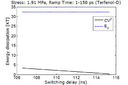
Figure 14 shows the energy dissipation as a function of switching delay for a fixed stress of 1.91 MPa. Once again, the delay is varied by varying the ramp’s rise (and fall) time between 1 and 150 ps. In this case, is nearly independent of the switching delay, meaning that the average power dissipation in the nanomagnet varies inversely with the switching delay. The ‘’ dissipation in the external circuit still goes down with increasing delay as expected because switching becomes increasingly ‘adiabatic’. This figure shows that we can switch in 110 ns by dissipating only 35 kT of energy at room temperature. The corresponding average power dissipation in this case is roughly 35 kT/110 ns = 1.33 pW per nanomagnet per bit flip. If we have an array of magnets with areal density 1010 cm-2 (10 Gbits/sq-cm) and 10% of them are being flipped at any given time (10% activity level), then the power dissipated is 1.3 mW/cm2. The energy needed to run at such low power levels can be harvested from the local surroundings using existing energy harvesting devices Roundy (2003); Anton and Sodano (2007); Lu et al. (2004); Jeon et al. (2005) without requiring a battery or external energy source! This opens up the possibility of unique applications such as medically implanted devices (e.g. processors implanted in a patient’s brain which warn of impending epileptic seizures) that run by harvesting energy from a patient’s body movements without requiring a battery, buoy mounted processors in the open sea that harvest energy from swaying motion induced by sea waves, or distributed sensor-processor networks for structural health monitoring of bridges and buildings that harvest energy from vibrations of the structure due to wind or passing traffic. These applications are made possible by the extreme energy efficiency of strain-induced switching.
IV.2 Nickel
Nickel has a negative magnetostrictive coefficient (see Table 1) so that a nickel/PZT multiferroic nanomagnet will require a tensile stress to initiate rotation away from the easy axis. However, the torque generated due to the change in stress with time (see Equations (II) and (20)) would be of same sign as that in the case of Terfenol-D since it depends on the product of the magnetostrictive coefficient () and the change in stress (). For the dimensions of the nanomagnet chosen, the minimum stress that we will need in a nickel/PZT multiferroic to switch is 57 MPa, while the maximum stress that can be generated by the 500 ppm strain in the PZT layer is 107 MPa.
IV.2.1 Ramp rate and switching delay
Just as in the case of Terfenol-D, Equations (II) and (20) are solved numerically to find the values of and at any given instant for the nickel/PZT nanomagnet. This yields the magnetization dyanmics under various stresses and ramp rates.
Fast ramp:
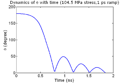
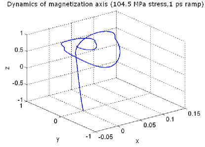
Figure 15 shows the magnetization dynamics of a nickel/PZT multiferroic nanomagnet when the stress is ramped up linearly in time from 0 to the maximum possible value of 107 MPa in 1 ps. The in-plane and out-of-plane dynamics of the magnetization vector are very similar to the case of Terfenol-D, except now we see a more ripples since there is more out-of-plane precession as can be seen in Figure 15(b). Nickel shows more ripples and more precession because it has a smaller Gilbert damping constant than Terfenol-D. Consequently, the precessional motion is less damped.
Slow ramp:
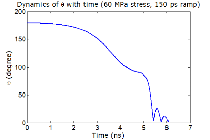
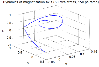
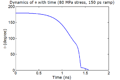
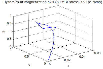
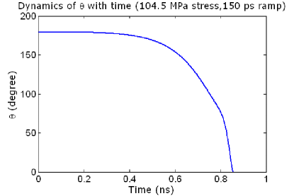
Figure 16(b) shows that a slow ramp rate (150 ps rise (and fall) time) quenches the precession of the magnetization vector. This happens because a slower ramp causes less out-of-plane excursion of the magnetization vector and hence less precessional motion. Note that contrary to expectation, the slow ramp (150 ps rise (and fall) time) completes the switching in 0.95 ns, while the fast ramp (1 ps rise (and fall) time) takes twice the amount of time, i.e. 1.9 ns! This happens because of the ripples and ringing which have a deleterious effect on switching speed. Note that both ramp rates make come very close to 1∘ in about 0.9 ns, but the faster ramp rate causes the magnetization vector to pull back from the final destination and vacillate before reaching the final destination. This causes the ringing which prolongs the switching duration and increases the delay.
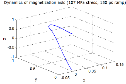
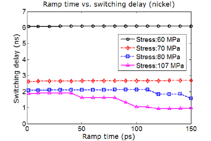
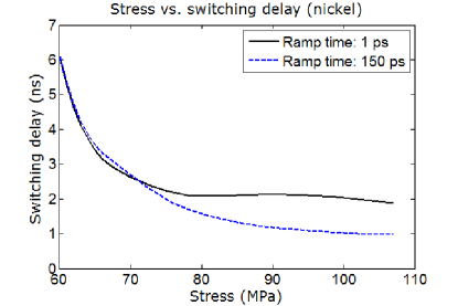
Figure 17 shows switching delay as a function of the ramp’s rise (and fall) time for various stresses. At higher stress levels (80 - 107 MPa), the switching delay actually decreases with increasing rise (and fall) time (a counter-intuitive result) because of the ripples that are generated when the stress is ramped up to high values very fast. Thus, the out-of-plane dynamics of the magnetization vector plays a vital role in switching.
For lower stress levels (60 -70 MPa), the switching delay increases slightly with increasing rise (or fall) time. Low stresses do not cause significant out-of-plane excursion of the magnetization vector leading to precessional motion. Therefore, even a fast ramp does not cause too many ripples and delay the switching when the stress is sufficiently low. In that case, a slower ramp will lead to slightly slower switching and that is what we observe.
Strangely, at slow ramp rates (e.g. rise (and fall) time = 150 ps) and low stress levels, a slightly lower stress can cause considerably more precession than a slightly higher stress which leads to very strong dependence of switching delay on the magnitude of stress at low stress levels. In order to illustrate this, we plot the switching dynamics for 150 ps rise (and fall) time in Figures 18 and 19, for stresses of 60 MPa and 80 MPa. There are ripples and considerable precessional motion when the stress is 60 MPa and virtually no ripple and very little precessional motion when the stress is 80 MPa. Thus, by increasing the stress slightly from 60 MPa to 80 MPa, the switching time can be reduced by a factor of four – from slightly above 6 ns to slightly above 1.5 ns.
The strong dependence of switching delay on stress at low stress levels is illustrated in Figure 20 which plots switching delay as a function of stress for two different rise (and fall) times of 1 ps and 150 ps. Notice that switching delay increases rapidly with decreasing stress in the interval [60 MPa, 70 MPa] but much less rapidly at higher stress levels exceeding 80 MPa. This is purely a consequence of the complex out-of-plane dynamics of the magnetization vector. This shows that any analysis which ignores the out-of-plane dynamics, and tacitly assumes that the motion of the magnetization vector will be always constrained to the plane of the nanomagnet since , will not only be quantitatively wrong, but qualitatively wrong as well.
The cross over between the two curves in Figure 20 was explained in the context of Terfenol-D and is not repeated here. This too is a consequence of the out-of-plane dynamics.
IV.2.2 Switching delay and energy dissipation
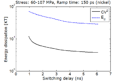
Figure 21 shows the energy dissipated in flipping the magnetization of the nickel/PZT multiferroic nanomagnet as a function of the switching delay. The latter is varied by varying the applied stress between 60 and 107 MPa with fixed rise (and fall) time of 150 ps for the stress ramp. The energy dissipated internally in the nanomagnet due to Gilbert damping and the ‘’ energy dissipated in the external circuit are shown separately. Both dissipation components decrease smoothly with increasing switching delay, implying that the average power dissipated during switching decreases rapidly with increasing delay. Both tend to saturate as the switching delay becomes longer.
In Figure 21, note that the ‘’ energy dissipated in the switching circuit is 1-2 orders of magnitude higher for nickel than for Terfenol-D for the same switching delay. Since the voltage is proportional to stress, the ‘’ energy is quadratically proportional to stress. Since the magnetostrictive coefficient of Terfenol-D is considerably higher than that of nickel, Terfenol-D requires much less stress to generate the same stress anisotropy energy and hence requires much less stress to switch. This results in a significant reduction of ‘’ energy dissipation in the case of Terfenol-D.
The total energy dissipation is however dominated by the energy dissipated internally in the nanomagnet due to Gilbert damping. This energy is actually smaller in nickel than in Terfenol-D, because the Gilbert damping constant of nickel is more than twice smaller than that of Terfenol-D. As long as we are switching adiabatically, will be the primary source of dissipation, and in that case, the material with the lower Gilbert damping constant will be superior since it will reduce total dissipation. The situation may change completely if we are switching abruptly. In that case, the ‘’ energy may very well be the major component of dissipation. If that happens, then the material with the larger magnetostrictive coefficient will be better since it will need less stress to switch and hence less voltage and less ‘’ dissipation. In other words, nickel is better than Terfenol-D (from the perspective of energy dissipation) when switching is adiabatic, but the opposite may very well be true when the switching is abrupt.
If speed is the primary concern, then what matters is the product of the magnetostrictive coefficient and the Young’s modulus. Since the maximum strain that can be generated in the magnetostrictive layer is fixed and determined by the PZT layer, the maximum stress anisotropy energy that can be generated in the magnet depends on the aforesaid product. The higher the stress anisotropy energy is, the faster will be the switching. Since the product is higher for Terfenol-D than for nickel, the Terfenol-D/PZT multiferroic switches faster. It can be switched in sub-ns by the maximum strain generated in the PZT layer, but that same strain cannot switch a nickel/PZT multiferroic in less than 1 ns.
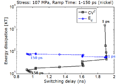
Figure 22 shows the energy dissipated as a function of switching delay when the latter is varied by varying the ramp’s rise (and fall) time between 1 ps and 150 ps, while holding the stress constant at 107 MPa. The ‘’ component decreases with increasing rise (and fall) time because switching becomes increasingly adiabatic. However, the dependence of on switching delay is more complicated. When the rise and fall of the ramp is fast, ripples appear. That causes the energy dissipation to increase with increasing delay contrary to expectation. This corresponds to the segment of the curve between switching delays of 0.9 to 1.9 ns which corresponds to rise times between 1 and 120 ps. At slower rise times between 120 and 150 ps, the ripples subside and the energy dissipation decreases with increasing delay. This corresponds to the segment between 0.9 ns and 1 ns switching delay.
IV.3 Cobalt
Cobalt has a negative magnetostrictive coefficient that is similar to nickel’s. Therefore, we will need a tensile stress to initiate magnetization rotation away from the easy axis. Its Gilbert damping constant is however smallest among the three materials considered (see Table 1) and hence we expect it to be least dissipative. For the dimensions of the nanomagnet chosen, the minimum stress that we will need in a cobalt/PZT multiferroic to switch is 56 MPa, while the maximum stress that can be generated by the 500 ppm strain in the PZT layer is 104.5 MPa.
IV.3.1 Ramp rate and switching delay
As before, Equations (II) and (20) are solved numerically to find the values of and at any given instant for the cobalt/PZT nanomagnet.
Fast ramp:
Figure 23 shows the magnetization dynamics of a cobalt/PZT multiferroic nanomagnet when the stress is ramped up linearly in time from 0 to the maximum possible value of 104.5 MPa in 1 ps. The in-plane and out-of-plane dynamics of the magnetization vector are very similar to the case of Terfenol-D or nickel, except now we see even more ripples and even more out-of-plane precession. Cobalt shows the most prominent ripples because it has the smallest Gilbert damping constant among all three ferromagnets considered. Hence, the precessional motion is least damped.
Slow ramp:
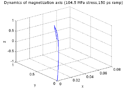
Figure 24 shows that a slow ramp rate (150 ps rise (and fall) time) quenches the precession of the magnetization vector. This happens because a slower ramp causes less out-of-plane excursion of the magnetization vector and hence less precessional motion. This reduces the switching delay from 1.6 ns in the case of 1 ps rise (and fall) time to 0.85 ns for 150 ps rise (and fall) time.
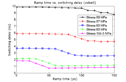
Figure 25 shows switching delay as a function of the ramp’s rise (and fall) time for various stresses. At all stress levels – not just at high stress levels as in the case of nickel – the switching delay decreases with increasing rise (and fall) time because of the ripples and the underlying precession that are generated when the stress is ramped up very fast. Unlike in the case of nickel, this happens even at small stress levels in cobalt since cobalt has the smallest Gilbert damping constant among the three and is hence most susceptible to precession.
IV.3.2 Switching delay and energy dissipation
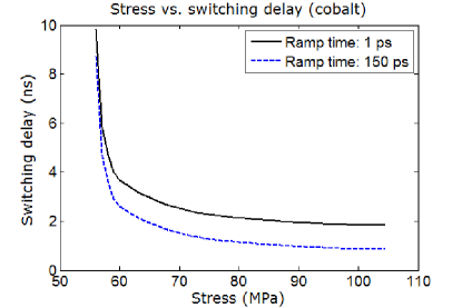
Figure 26 shows the dependence of switching delay on stress for two different ramp rise (and fall) times of 1 ps and 150 ps. As expected, the switching delay has a very weak dependence on the rise (and fall) time at small stress levels when not too much ringing occurs. However, at high stress levels, the switching delay increases considerably for the shorter ramp time since that causes prolonged ringing associated with precessional motion. This is a more pronounced effect for cobalt than for nickel or Terfenol-D since cobalt has the smallest Gilbert damping constant among all three that makes it particularly susceptible to precessions.
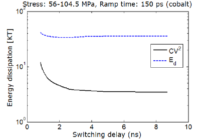
Figure 27 shows the energy dissipated in flipping the magnetization as a function of switching delay when the latter is varied by varying the stress between 56 MPa and the maximum possible 104.5 MPa. Both the internal energy dissipation and the energy dissipated in the switching circuit ‘’ decreases with increasing delay showing that the average power dissipated decreases quite rapidly with increasing delay. Overall, the energy dissipation is slightly less here than in nickel because cobalt has the lower Gilbert damping constant and slightly higher saturation magnetization (see Equation (25). Once again, the dissipated energies saturate at long delays.
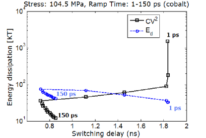
Figure 28 plots the energy dissipations as a function of the switching delay when the latter is varied by monotonically varying the rise time of the ramp from 1 to 150 ps, while holding the stress constant at 104.5 MPa. For the plot, there are two segments. In the first segment spanning the range of switching delay between 0.75 ns and 1.8 ns, the ramp’s rise (and fall) time was varied from 1 ps to 50 ps. In this interval, the switching delay decreases with increasing rise (and fall) time because of the ripple effect (see Figure 25 and the 104.5 MPa stress curve). In this interval, the energy dissipated internally in the magnet goes up with increasing ramp time since we are switching faster, but the ‘’ energy dissipated in the external circuit goes down since switching is becoming more adiabatic (rise time is longer)111Note that adibaticity of switching is not determined by the switching delay, but by the rise (and fall) time of the ramp.. The second segment spanning the switching delay range between 0.75 and 0.85 ns corresponds to rise (and fall) time between 50 ps and 150 ps. In this range of rise (and fall) times, the switching delay increases with increasing rise (and fall) time because the ripples subside (see Figure 25 again and the 104.5 MPa stress curve). In this range, goes down with increasing ramp time since we are switching slower. The ‘’ energy dissipation of course always decreases with increasing rise (and fall) time since the switching becomes increasingly adiabatic.
V Discussions
We have analyzed the switching dynamics in a multiferroic nanomagnet consisting of a PZT layer and a magnetostrictive layer subjected to time-varying stress. The stress is ramped up linearly in time with different rates or rise (and fall) times. Three different materials (Terfenol-D, nickel, cobalt) were considered for the magnetostrictive layer. They show different behavior because of different material parameters (Youngs’ modulus, magnetostrictive coefficient and Gilbert damping).
For the type of magnets chosen (materials and dimensions), the minimum switching delay that we have found is 252 ps obtained with Terfenol-D using a rise (and fall) time of 60 ps for a compressive stress of 40 MPa. The corresponding ‘’ energy dissipation in the switching circuit is 30 kT and the energy dissipated internally in the nanomagnet due to Gilbert damping is = 777 kT. For nickel, the minimum switching delay is 930 ps obtained with a stress of 107 MPa and a rise (and fall) time of 120 ps. In this case, the ‘’ energy dissipation in the switching circuit is 15 kT and the energy dissipated internally in the nanomagnet due to Gilbert damping is = 79 kT. Finally, for cobalt, the minimum switching delay is 723 ps obtained with a stress of 104.5 MPa and a rise (and fall) time of 50 ps. The ‘’ energy dissipation in the switching circuit is 36 kT and the energy dissipated internally in the nanomagnet due to Gilbert damping is = 75 kT.
All this shows that it is possible to switch multiferroic nanomagnets in less than 1 ns while dissipating energies of 100 kT. This range of energy dissipation is far lower than what is encountered in spin transfer torque based switching of nanomagnets with the same switching delay. Thus, strain induced switching of magnets has the potential to emerge as the preferred method of switching magnetic bits in magnet-based non-volatile logic and memory.
References
- (1) K. Roy, J. Atulasimha, and S. Bandyopadhyay, arXiv:1101:2222 .
- (2) N. D’Souza, J. Atulasimha, and S. Bandyopadhyay, arXiv:1101:0980 .
- Atulasimha and Bandyopadhyay (2010) J. Atulasimha and S. Bandyopadhyay, Appl. Phys. Lett. 97, 173105 (2010).
- (4) M. S. Fashami, K. Roy, J. Atulasimha, and S. Bandyopadhyay, Nanotechnology (accepted), arXiv:1011:2914 .
- Brintlinger et al. (2010) T. Brintlinger, S. H. Lim, K. H. Baloch, P. Alexander, Y. Qi, J. Barry, J. Melngailis, L. Salamanca-Riba, I. Takeuchi, and J. Cumings, Nano Lett. 10, 1219 (2010).
- Wolf et al. (2010) S. A. Wolf, J. Lu, M. R. Stan, E. Chen, and D. M. Treger, Proc. IEEE 98, 2155 (2010).
- Zavaliche et al. (2007) F. Zavaliche, T. Zhao, H. Zheng, F. Straub, M. P. Cruz, P. L. Yang, D. Hao, and R. Ramesh, Nano Lett. 7, 1586 (2007).
- Eerenstein et al. (2006) W. Eerenstein, N. D. Mathur, and J. F. Scott, Nature 442, 759 (2006).
- Nan et al. (2008) C. W. Nan, M. I. Bichurin, S. Dong, D. Viehland, and G. Srinivasan, J. Appl. Phys. 103, 031101 (2008).
- Atulasimha et al. (2008) J. Atulasimha, A. B. Flatau, and J. R. Cullen, J. Appl. Phys. 103, 014901 (2008).
- Chikazumi (1964) S. Chikazumi, Physics of Magnetism (Wiley New York, 1964).
- Beleggia et al. (2005) M. Beleggia, M. D. Graef, Y. T. Millev, D. A. Goode, and G. Rowlands, J Phys. D: Appl. Phys. 38, 3333 (2005).
- Nikonov et al. (2010) D. E. Nikonov, G. I. Bourianoff, G. Rowlands, and I. N. Krivorotov, J. Appl. Phys. 107, 113910 (2010).
- Abbundi and Clark (1977) R. Abbundi and A. E. Clark, IEEE Trans. Magn. 13, 1519 (1977).
- Ried et al. (1998) K. Ried, M. Schnell, F. Schatz, M. Hirscher, B. Ludescher, W. Sigle, and H. Kronmüller, Phys. Stat. Sol. (a) 167, 195 (1998).
- Kellogg and Flatau (2008) R. Kellogg and A. Flatau, J. Intell. Mater. Sys. Struc. 19, 583 (2008).
- Walowski et al. (2008) J. Walowski, M. D. Kaufmann, B. Lenk, C. Hamann, J. McCord, and M. Münzenberg, J Phys. D: Appl. Phys. 41, 164016 (2008).
- (18) http://www.allmeasures.com/Formulae/static/materials/.
- Lisca et al. (2006) M. Lisca, L. Pintilie, M. Alexe, and C. M. Teodorescu, Appl. Surf. Sci. 252, 4549 (2006).
- (20) http://www.memsnet.org/material/leadzirconatetitanatepzt/.
-
(21)
http://www.itrs.net/Links/2009ITRS/
2009Chapters_2009Tables/2009_Interconnect.pdf. - Sun and Wang (2005) Z. Z. Sun and X. R. Wang, Phys. Rev. B 71, 174430 (2005).
- Behin-Aein et al. (2009) B. Behin-Aein, S. Salahuddin, and S. Datta, IEEE Trans. Nanotech. 8, 505 (2009).
- (24) http://www.itrs.net.
- Fukami et al. (2009) S. Fukami, T. Suzuki, K. Nagahara, N. Ohshima, Y. Ozaki, S. Saito, R. Nebashi, N. Sakimura, H. Honjo, K. Mori, C. Igarashi, S. Miura, N. Ishiwata, and T. Sugibayashi, in VLSI Technology, 2009 Symposium on (IEEE, 2009) pp. 230–231.
- Roundy (2003) S. Roundy, Ph.D. thesis, Mech. Engr., UC-Berkeley (2003).
- Anton and Sodano (2007) S. R. Anton and H. A. Sodano, Smart Mater. Struct. 16, R1 (2007).
- Lu et al. (2004) F. Lu, H. P. Lee, and S. P. Lim, Smart Mater. Struct. 13, 57 (2004).
- Jeon et al. (2005) Y. B. Jeon, R. Sood, J. Jeong, and S. G. Kim, Sens. Act. A: Phys 122, 16 (2005).
- Note (1) Note that adibaticity of switching is not determined by the switching delay, but by the rise (and fall) time of the ramp.