Tunneling states in graphene heterostructures consisting of two different graphene superlattices
Abstract
We have theoretically investigated the properties of electronic transport in graphene heterostructures, which are consisted of two different graphene superlattices with one-dimensional periodic potentials. It is found that such heterostructures possess an unusual tunneling state occurring inside the original forbidden gaps, and the electronic conductance is greatly enhanced and Fano factor is strongly suppressed near the energy of the tunneling state. Finally we present the matching condition of the impedance of the pseudospin wave for occuring the tunneling state by using the Bloch-wave expansion method.
pacs:
73.21.-b, 73.20.At, 73.21.Cd, 73.22.PrI Introduction
Graphene has attracted a lot of attention since its discovery in 2004 Novoselov2004 . The linear dispersion property near the Dirac point leads the low-energy charge carriers obeying the massless relativistic Dirac equation. Thus many unique electronic and transport properties such as half-integer quantum Hall effect Gusynin2005 ; Purewal2006 and Klein paradox Katsnelson2006 are demonstrated in graphene.
Currently, most investigations are focused on the properties of graphene itself. There are only a few works on graphene-based heterostructures, for example, gated graphene heterostructures Ryzhii2006 , graphene nanoribbon heterostructures Rosales2008 , and graphene/hexagonal-BN heterostructures Bjelkevig2010 . Heterostructures are usually referred to the combination of two different materials/structures Kroemer1963 . According to the analog between the one-dimensional photonic crystals containing left-handed metamaterials Li2003 ; JiangHT2003 ; Shadrivov2003 and the graphene-based one-dimensional periodic superlattices Barbier2010 ; Arovas2010 ; Wang2010a , many optical properties may be introduced into the graphene-based electronic systems. In this paper, we will theoretically study the graphene heterostructures consisted of two different graphene-based superlattices (GSs), which can be constructed by electrostatic Bai2007 ; Barbier2008 ; Park2008 ; Brey2009 ; Park2009 ; Park2008b or magnetic barriers RamezaniMasir2008 ; Ghosh2009 . Since the electronic pseudospin wave may be highly localized at the interface between two different GSs, it would be expected that such heterostructures may possess an unusual tunneling mode inside the zero-averaged wave-number gap Wang2010a . The location of such a tunneling state satisfies the impedance matching condition of the electronic pseudospin wave.
II Theoretical Formula
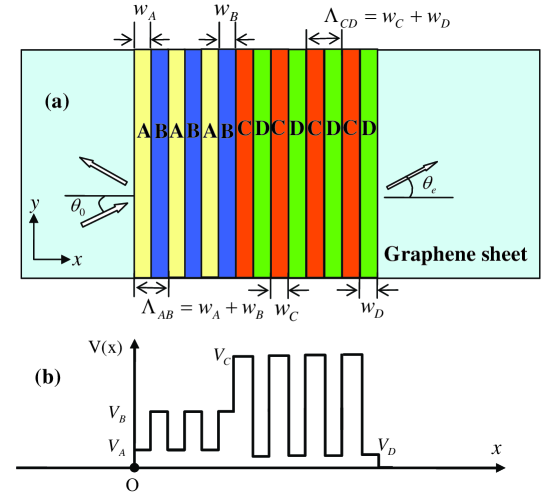
Now let us consider an electron of energy and wavevector (with the Fermi velocity m/s) be incident at an angle onto a graphene heterostructure , as shown in Fig. 1, where , , and indicate different potentials, and and are the period numbers. As we know that the Hamiltonian of a low-energy electron in graphene is given by , here is a momentum operator, , and are Pauli matrices, is a unit matrix, and is the th electrostatic potential. This Hamiltonian acts on a two-component pseudospin state where and are two components of the pseudospin wave (here we omit the term due to the translation invariance in the direction). Therefore, the wavefunctions at and inside the th potential can be related via a transfer matrix: Wang2010a
| (1) |
where sign is the component of the wavevector for , otherwise . Using the boundary conditions, both the reflection and transmission coefficients could be obtained by the transfer matrix method, Wang2010a
| (2) | |||||
| (3) |
where , , is an exit angle (see Fig. 1), and are the elements of the total transfer matrix from the incident to exit ends. Once the coefficients and are obtained, the total conductance of the system at zero temperature can also be calculated by using the Büttiker formula Datta1995 , , where is the transmittivity and , and is the width of the graphene strip in the direction. Furthermore, the Fano factor in this system is given by Tworzydlo2006 . Therefore the reflection, transmission, conductance, and Fano factor inside such graphene-based heterostructures can be obtained by numerical calculations.
III Numerical Results
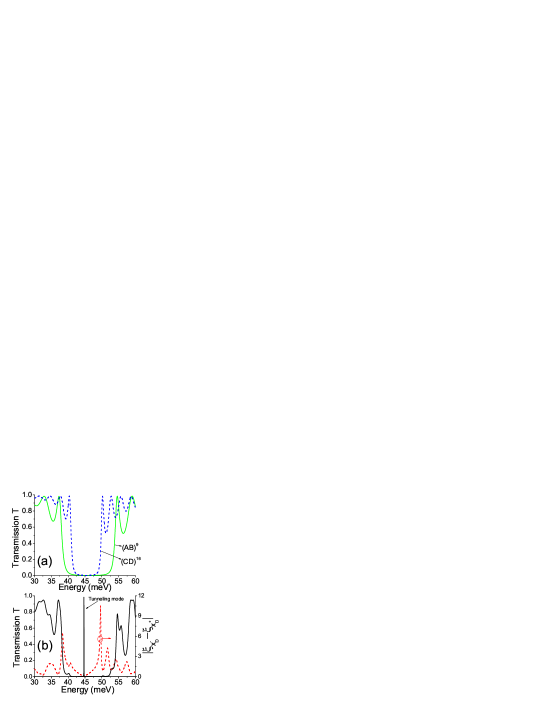
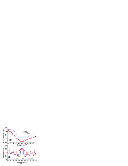
Based on the above formulae, we can calculate the changes of the transmission, conductance and Fano factor of an electron passing through the heterostructures. In Fig. 2 and Fig. 3, we show the typical electronic transmission, conductance and Fano factor for different situations with the parameters , , meV, meV, meV, meV, and nm. For a single GS or , from Fig. 2(a) and Fig. 3, the forbidden gaps do exist near the new Dirac point at meV, which is called the zero-averaged wave-number gap in Ref. Wang2010a , and the corresponding conductance is minimal and the Fano factor equals to 1/3 at the new Dirac point of meV for both cases of and . Here we would like to point out that the condition for appearing the Dirac point inside the GSs are discussed in detail in Refs. Barbier2010 ; Arovas2010 ; Wang2010a . For a special case with and , the condition is simply given by and derived from Eq. (41) in Ref. Wang2010a .
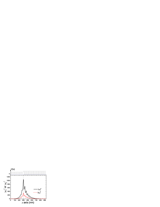
However, for the heterostructure , see Fig. 2(b), a new tunneling mode occurs inside the forbidden gap near the Dirac point. Due to the existence of this tunneling mode, compared with the case of the individual or , for the heterostructure the electronic conductance is greatly enhanced and the Fano factor is strongly suppressed, as shown in Figs. 3(a) and 3(b). In fact, this new tunneling mode is due to the formation of the highly localized state at the interface between and , which could be clearly seen from the density distributions of the electronic pseudospin wavefunctions in Fig. 4. The probability densities are highly localized at the interface between and , which is denoted by the vertical dot line.
IV Matching condition of the tunneling mode in forbidden gaps
In order to obtain the condition of this new tunneling mode, we use the so-called matching condition of the impedance of the pseudospin wave. In infinite periodic barriers, obeys the Bloch-Floquet theorem. By using the Bloch-wave expansion method in Ref. Kang2009 , inside the GS or , can be written as
| (4) |
where is the component of the pseudospin Bloch-wave vector and satisfies the eigen equation: [ is the matrix of the unit cell for or with or ], and is the length of unit cell. are the eigenvectors of corresponding to the eigenvalues , and are the amplitudes of the forward (+) and backward (-) Bloch waves. From Ref. Wang2010a , at both the incident and exit regions can be, respectively, expressed by and , where and are the impedances at the incident and exit ends, and is the incident wavefunction. Inside the GS , from Eq. (4), we can define and where is the impedance at and is the impedance at the interface (), and () is a coefficient. Therefore, we can obtain
| (5) |
with . Similarly, the impedance of the pseudospin wave at inside the GS is given by
| (6) |
where . For a perfect tunneling mode in heterostructures, when and only when the impedances of the pseudospin waves at two sides of the interface between and satisfy
| (7) |
the zero reflection can be exactly reached. In this case, the reflection coefficient is also zero, i. e., , thus at the incident end, and at the exit end. For the imperfect tunneling process, the condition of Eq. (7) should be replaced by . In Fig. 2(b), we plot the curve for the value of , see the dashed line. From Fig. 2(b), it is clear that when the value of is close to zero (within the original forbidden gaps), there is a tunneling peak with near-unity transmittance. According to the analog between one-dimensional photonic crystal heterostructures Kang2009 and the graphene-based heterostructure consisted of two different superlattices, we could safely say that in our case the tunneling state is the electronic Tamm state. It should be mentioned that, for the other zeroes of (which are located outside of the original forbidden gaps), they correspond to the resonances of the propagation states, rather than the localized states.
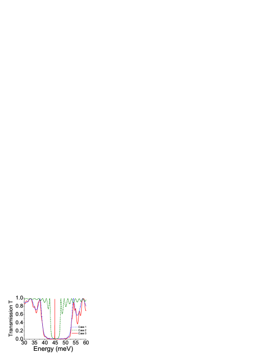
So far we only consider the GSs consisted of square barriers and wells. In fact, the above results about the tunneling state will also occur inside the graphene heterostructures, which are consisted of other periodic potentials such as cosine or sine potentials Brey2009 . For a comparison, in Fig. 5, we also plot the electronic transmittance for the heterostructures consisted of different sine potentials. It is clearly seen that the new tunneling state also appears inside the original forbidden gaps under the optimal period numbers.
V Conclusion
In summary, we have investigated the electronic transport inside the graphene-based heterostructures consisted of two different GSs. It is shown that in such heterostructures there is an unusual tunneling state inside the zero-averaged wave-number gaps, which leads to the enhancement of the electronic conductance and the suppression of the Fano factor. The reason of occurring such a tunneling state is due to the highly localization of the electronic pseudospin wave at the interface between two GSs. Finally the matching condition of the impedance of the pseudospin wave is analytically presented. The parameters used in our study are technically feasible as demonstrated in experimental studies Meyer2008 ; Marchini2007 ; VazquezdeParga2008 ; Pan2009 . For example, in Ref. Meyer2008 , superlattice patterns with periodicity as small as 5 nm have been imprinted on graphene using the electron-beam induced deposition. The phenomenon for occurring such a tunneling state in graphene heterostructures is potentially useful in filtering single-energy electron and is also hopefully to use in the design of graphene-based electronic devices Peres2010 .
Acknowledgements.
This work is supported by the National Natural Science Foundation of China (No. 61078021) and Hong Kong RGC Grant No. 403609.References
- (1) K. S. Novoselov, A. K. Geim, S. V. Morozov, D. Jiang, Y. Zhang, S. V. Dubonos, I. V. Grigorieva, and A. A. Firsov, Science, 306, 666(2004).
- (2) V. P. Gusynin and S. G. Sharapov, Phys. Rev. B 71, 125124 (2005).
- (3) M. S. Purewal, Y. Zhang and P. Kim, Phys. Status Solidi B 243, 3418 (2006).
- (4) M. I. Katsnelson, K. S. Novoselov and A. K. Geim, Nature Physics 2, 620 (2006).
- (5) V. Ryzhii, Jpn. J. Appl. Phys. 45, L923 (2006); V. Ryzhii, VA. Sato, and T. Otsuji, J. Appl. Phys. 101, 024509 (2007).
- (6) L. Rosales, P. Orellana, Z. Barticevic, M. Pacheco, MicroElectronics Journal, 39, 537-540 (2008).
- (7) C. Bjelkevig, Z. Mi, J. Xiao, P. A. Dowben, L. Wang, W. N. Mei, and J. A. Kelber, J. Phys.: Condens. Matter 22, 302002 (2010).
- (8) H. Kroemer, Proceedings of the IEEE, vol. 51, pp.1782-1783 (1963).
- (9) J. Li, L. Zhou, C. T. Chan, and P. Sheng, Phys. Rev. Lett. 90, 083901 (2003).
- (10) H. T. Jiang, H. Chen, H. Q. Li, Y. W. Zhang and S. Y. Zhu, Appl. Phys. Lett. 83, 5386 (2003).
- (11) I. V. Shadrivov, A. A. Sukhorukov, and Y. S. Kivshar, Appl. Phys. Lett. 82, 3820 (2003).
- (12) M. Barbier, P. Vasilopoulos, and F. M. Peeters, Phys. Rev. B. 81, 075438 (2010).
- (13) L.-G. Wang and S.-Y. Zhu, Phys. Rev. B 81, 205444 (2010).
- (14) D. P. Arovas, L. Brey, H. A. Fertig, E.-A. Kim, and K. Ziegler, arXiv:1002.3655V2 (2010).
- (15) C. Bai and X. Zhang, Phys. Rev. B 76, 075430 (2007).
- (16) M. Barbier, F. M. Peeters, P. Vasilopoulos, and J. Milton Pereira, Jr., Phys. Rev. B 77, 115446 (2008).
- (17) C. -H. Park, L. Yang, Y.-W. Son, M. L. Cohen and S. G. Louie, Nature Physics 4, 213 (2008).
- (18) L. Brey and H. A. Fertig, Phys. Rev. Lett. 103, 046809 (2009).
- (19) C.-H. Park, Y.-W. Son, L. Yang, M. L. Cohen, and S. G. Louie, Phys. Rev. Lett. 103, 046808 (2009).
- (20) C.-H. Park, L. Yang, Y.-W. Son, M. L. Cohen, and S. G. Louie, Phys. Rev. Lett. 101, 126804 (2008)
- (21) M. Ramezani Masir, P. Vasilopoulos, A. Matulis, and F. M. Peeters, Phys. Rev. B 77, 235443 (2008).
- (22) S. Ghosh and M. Sharma, J. Phys.: Condens. Matter 21, 292204 (2009).
- (23) S. Datta, Electronic Transport in Mesoscopic Systems, Cambridge University Press, 1995.
- (24) J. Tworzydło, B. Trauzettel, M. Titov, A. Rycerz, and C. W. J. Beenakker, Phys. Rev. Lett. 96, 246802 (2006).
- (25) X. B, Kang, W. Tan, Z. G. Wang, and H. Chen, Phys. Rev. A 79, 043832 (2009).
- (26) J. C. Meyer, C. O. Girit, M. F. Crommie, and A. Zettl, Appl. Phys. Lett. 92, 123110 (2008).
- (27) S. Marchini, S. Günther, and J. Wintterlin, Phys. Rev. B 76, 075429 (2007).
- (28) A. L. Vazquez de Parga, F. Calleja, B. Borca, M. C. G. P. Jr, J. J. Hinarejo, F. Guinea, and R. Miranda, Phys. Rev. Lett. 100, 056808 (2008).
- (29) Y. Pan, H. Zhang, D. Shi, J. Sun, S. Du, F. Liu, and H.-J. Gao, Adv. Mater. 21, 2777 (2009).
- (30) N. M. R. Peres, Rev. Mod. Phys. 82, 2673 (2010).
Figure Captions
Fig. 1. (Color online) (a) Schematic of a heterostructure consisted of two different graphene superlattices, and . (b) The schematic profiles of the potentials.
Fig. 2.(Color online) Electronic transmittances through (a) the individual graphene superlattice or and (b) the heterostructure , with . In (b), the dashed line denotes the value of . The parameters are meV, meV, meV, meV, nm, , and .
Fig. 3. (Color online) Changes of (a) conductance and (b) Fano factor in different structures. Other parameters are the same as in Fig. 2.
Fig. 4.(Color online) Changes of probability densities inside the heterostructure, at the energy of the tunneling mode, meV, and . Other parameters are the same as in Fig. 2.
Fig. 5. (Color online) Electronic transmittances through different structures with the incident angle : Case 1, meV for nm; Case 2, meV for nm; Case 3, the combination of Cases 1 and 2.