Manganese valence and magnetotransport in ultrathin films of La0.67Ca0.33MnO3
Abstract
We report a comparative study of the properties of very thin films of La0.67Ca0.33MnO3 grown epitaxially under strain on flat SrTiO3 (STO), lattice matched on NdGaO3 (NGO), and strained on -miscut STO. We use transmission electron microscopy and electron energy loss spectroscopy to study the microstructure, composition, and Mn valence state. Near the interface we find no significant segregation, but a charge compensation layer where the valence is enhanced over the nominal value of 3.3+, and a relaxation to this value over several nanometer. The transport properties show well-known behavior for the films on flat STO and NGO, namely values of the metal-insulator transition temperature which are strongly (STO) or only little (NGO) reduced with respect to the bulk value. The reduction in films on miscut STO however is less strong than in films on flat STO, even though they appear similar as to strain state and interface layer. Magnetically, we find reduced values of the saturation magnetization for the strained films with respect to the bulk value, which cannot only be ascribed to the interface layer.
I Introduction
Transition metal oxides with the perovskite structure are strongly correlated electron systems which show diversity in physical properties caused by the competition between charge, spin and orbital degrees of freedom. Much work has been done in the last decade to understand the rich underlying physics of the correlated and semi-localized 3d electrons and their interaction with the lattice. In particular for the manganites, showing the colossal magnetoresistance effect (CMR) connected to the combined metal-insulator (MI) and paramagnetic-to-ferromagnetic transition, much progress has been made, as can be found in a number of reviews tokura06 ; dagotto08 ; salamon01 . Still, even in bulk materials the picture is still being refined, as was for instance shown recently in the discovery of the existence of glassy correlated phases in single crystals of optimally doped La0.7Ca0.3MnO3 lynn07 . Also for thin films, a large amount of work has gone into basic questions on their physical properties, with the possibility of strain engineering as an issue of special interest. In bulk manganites of the type (REAxMnO3 (RE is a 3+ Rare Earth ion, A is a 2+ alkaline ion) and at fixed RE to A ratio and therefore the Mn3+ to Mn4+ ratio, the properties can be changed by varying the radius of the 2+ ion. This is basically because the ion radius influences the structure of the coupled network of MnO6 octahedra, which changes the balance between the itinerancy of the Mn 3 electrons, and the strength of the Jahn-Teller distortions which tend to trap electrons on the Mn sites. In films this effect can be amplified by growing on a substrate with a different lattice parameter, thereby putting the film under tensile or compressive strain. For instance in films of La0.7Ca0.3MnO3 (LCMO; pseudocubic lattice parameter = 0.386 nm) on SrTiO3 (STO; = 0.391 nm) the temperature of the metal-insulator transition TMI goes down to 110 K for films with a thickness of around 10 nm, compared to a bulk value of 260 K aarts98 ; bibes01 ; yang04 . Below about 5 nm the MI transition rather abruptly disappears, mainly because the large strain leads to different crystal structures in the film yang04 . At the same time, magnetic measurements indicate the presence of a dead layer in the LCMO/STO system of a few nm and nanoscale phase separation bibes01 , and also in general a lowered value of the saturation magnetization for larger thicknesses aarts98 .
Gaining more understanding about these ultrathin films in the regime around 10 nm is of obvious interest. In principle they are suitable as gated devices, since SrTiO3 is a highly polarizable dielectric, but then more needs to be known about the electronic structure of the film close to the interface. This is of particular interest since the Mn-valency may be influenced by discontinuities in the charge variation, as is now under extensive investigation for the case of SrTiO3 / LaAlO3 ohtomo04 . Another question is the role of disorder and strain relaxation. Here we present a comparative study of LCMO films grown on flat SrTiO3 (STO; tensile strain), NdGaO3 (NGO; strain-free) substrates as well as of on STO substrates which have an intentional misorientation of the surface normal of 1∘ towards the [010] direction, which leads to a stepped structure with a terrace length of about 25 nm. We investigate the microstructure, the atomic composition, and the Mn-valence state using High Resolution Transmission Electron Microscopy (HR-TEM), and Electron Energy Loss Spectroscopy (EELS), but also the magnetic and magnetotransport properties of these same films. We find that basically all films show the bulk structure. For films on both flat and miscut STO, the Mn-valence is slightly higher at the interface (about 0.1 electron charge), and drops to the bulk value within 3 to 5 nm. For films on NGO we find the same, which suggests that it is neither a different crystal structure, nor strain, but rather the change in charge distribution when going from substrate to film which is driving this variation. We then show from transport data that these film show the same trends in as found before, with a strong drop for films on flat STO and a small variation for films on NGO. We also find that for films on miscut STO stays significantly higher. Finally we come back to the issue of magnetization and show that the saturation values for films in this thickness regime are lower than can be expected on the basis of the non-bulk interface layer alone.
II Experimental
Epitaxial films of LCMO with thicknesses between 47 nm and 6 nm were grown on (001) STO substrates, by DC sputtering in oxygen pressure of 300 Pa at a growth temperature of 840 ∘C. The substrates have a misorientation of either 0.2∘ in random direction which we denote as flat STO or 1∘ towards [010] direction. Here we define the nomenclature which we will use throughout this paper to refer to our films. Films grown on flat STO are indicated by L(), with the film thickness (rounded to the nearest integer value), films grown on misoriented STO by L()mis and films on NGO, by L()NGO. Before and after film growth we used Atomic Force Microscopy (AFM) to asses the quality of the STO substrate and the LCMO film (see Fig.1).
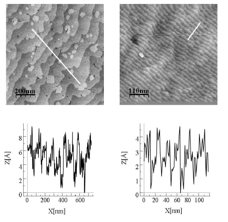
One issue to be discussed is the surface termination of the STO, which can be either a TiO2- or an SrO-layer. Commercial substrates have mixed termination but can be treated to become singly terminated, with the TiO2 surface easier to fabricate and more stable. Whether this is of influence on the film properties that are investigated in this paper will be discussed later. All films show clear unit-cell high step edges. The films grown on flat STO show an average terrace length of 75 nm and the films grown on misoriented STO show an average terrace length of 20 nm, identical to the terrace length of the substrate (see Fig. 1). The thickness, growth rate and lattice parameters of the LCMO films were determined by x-ray reflectivity (XRR) and reciprocal space mapping (RSM) measurements, respectively. The average growth rate of our LCMO thin films is 0.8 nm/min, which results in films with roughness of the order of the dimensions of the unit cell.
We have characterized the microstructure, the atomic composition, and the Mn-valence state of LCMO thin films using the HR-TEM (High Resolution Transmission Electron Microscopy) and EELS (Electron Energy Loss Spectroscopy) techniques. We will show results of LCMO films grown on STO (flat), STO (1∘) and NGO. HR-TEM specimens were prepared according to a standard cross-section preparation method. Before insertion into the microscope, the specimens were plasma-cleaned for 1 minute to prevent carbon contamination during the experiments. The analysis was performed with a FEI TITAN equipped with a spherical aberration (C) corrector and a High Resolution Gatan Image Filter (HR-GIF) operated at 300kV. EELS data were collected in scanning TEM mode with a probe size of about 0.2 - 0.5 nm. The spectra were acquired by probing the same region only once to reduce the beam-induced damage. The energy dispersion was 0.1 eV/channel for the Zero Loss Peak and 0.2 eV/channel for the Mn L-edge to obtain more signal.
The magnetotransport properties were studied by measuring the current () - voltage () characteristics as function of temperature and in high magnetic fields. We used a PPMS (Physical Properties Measurement System, Quantum Design) for temperature control (T = 20 - 300 K) and for magnetic field control (Ha = 0 - 9 T), in combination with an external current source and nanovoltmeter. For the magnetization measurements we used an MPMS (Magnetic Properties Measurement System, Quantum Design) with T = 10 - 300 K and Ha = 0 - 5T.
III Microstructure and Mn valency
III.1 Microstructure
From HR-TEM investigations on several specimens for each film we find that our films are epitaxial. The perovskite crystal structure of the films is close to cubic with lattice parameter ac = 0.39 nm, but due to small rotations of the oxygen octahedra it becomes orthorhombic (space group: ). Using electron diffraction we observed that throughout the films the bulk structure is present with lattice parameters of , 2 and .
 |
 |
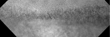 |
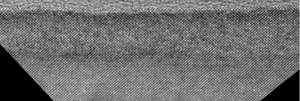
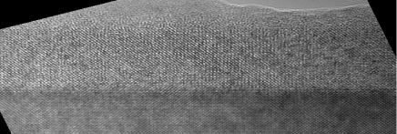
For most films, the axis was found to be parallel to the interface normal (with length 2 in pseudocubic notation lat ). In HR-TEM mode (see Fig.2), and scanning along the interface, we did not observe any antiphase boundaries or any domain type disorder, which is in line with previous reports yang3a . The amorphous layer visible at the top surface of the thin film in Fig.2 (top image) is glue used during preparation of the sample. The HR-TEM images shown in Fig.2 (samples L(6), L(10) and L(7)) all show a fully epitaxial thin film. There is a special reason to show a micrograph for sample L(10), since this film has deviating properties compared to the typical film on flat STO, as will be shown later. HREM on this film showed no differences compared to the other films. We also observe that films grown on 1∘ misoriented STO (Fig.2c) are epitaxial with no clear influence of the step edges on the microstructure of the LCMO film. We also do not observe any misfit dislocation at the film-substrate interface in any of the films, which were investigated with HR-TEM.
III.2 Mn-oxidation state and elemental composition
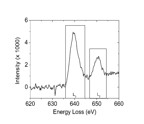
We have used EELS to investigate the composition and the Mn-oxidation state across the thickness of our thin films. In an EELS measurement the sample is exposed to an electron beam with a well defined (small range of) kinetic energies. While the electrons go through the sample, inelastic interactions (i.e. atom core loss, inner shell ionization) result in the loss of kinetic energy, which can be measured using an electron spectrometer. An EELS spectrum consists of a Zero Loss peak (ZLP), and subsequent peaks at lower energy corresponding to different losses due to interaction with the sample. An example of an EELS spectrum at the Mn L-edge is given in Fig.3. The L2 and L3 peaks are indicated, and used to determine the Mn valence. The raw EELS data were corrected for specimen thickness, which influences the ratio between intensities of ZLP peak and the rest of the spectrum thickness3 . From the data it can be assumed that the elemental composition will not have any dependence on the specimen thickness. Since the only interest is to qualitatively monitor the changes across the film, the cross section was taken as a constant. By acquiring the ZLP, Mn L-edge and the La K-edge at 100 eV and calculating the ratio between the various integrals, the Mn-valence and the elemental concentration across the film thickness are obtained. The L32 ratio, correlated to the Mn-valence, is determined from the integrated intensities ratio L3/L2. Ratios of 2.1 and 2.7 correspond to Mn4+ and Mn3+, respectively; the calculated valence for La0.7Ca0.3MnO3 is 3.3+ for bulk specimens Gianluigi3 . Acquiring spectra across the film yields elemental and valence profiles.
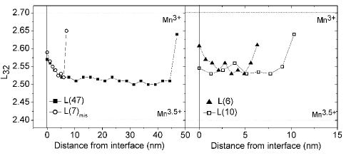
In Fig.4 the calculated L32 ratio is shown for several films grown on
STO. Three regions can be discerned. At the film surface (interface with vacuum) the
Mn-valence is reduced towards 3+. In the bulk of the film, particularly visible in
L(47), the L32 ratio indicates a Mn-valence close to 3.3+, similar to the value
for bulk LCMO. Close to the interface with the STO substrate a reduction in
Mn-valence is observed. With the probe placed on the first layer the valence is
equal to 3.2+ in both L(6) and L(47). The presence of this reduction is typical for
our LCMO films grown on STO substrates, but the extent of the reduction varies
between 2 - 5 nm for different films. A similar reduction is also found for
L(7)mis, grown on 1∘ miscut STO. The step edges on the STO surface
appear to have no significant influence on the Mn-oxidation state near the substrate
interface. Therefore, these properties are general features of LCMO films grown by
sputtering on STO substrates. Fig.4 also shows sample L(10), however, which
did not show the reduced ratio at the substrate interface. The precise cause of this
remains unclear, especially since HR-TEM does not indicate a different type of
interface.
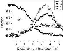
We also used EELS to map the elemental composition across the films. As shown in
Fig. 5 for L(6) and L(10), the composition (for the most part) is close to
that of the sputtering target. The apparent interdiffusion of Ti4+ into the
film is caused by the limited resolution (determined by the beam size) of the
measurement. Other films showed a similar profile. In particular, we do not find
cation segregation at the interface, as a possible cause for the deviation of the
Mn-valence with respect to the bulk value of the film. One exception was sample
L(47), where we observed La enrichment near the film-substrate interface. However,
since the results for all other samples did not show such segregation, it is likely
that the observed La-enrichment is not correlated with the observed Mn-valence
reduction.
 |
 |
An important question is whether the valence reduction at the interface is caused by strain. We therefore investigated the Mn-valence profile and elemental composition in LCMO films grown on NGO substrates as well. The results, plotted in Fig. 6, show that also for films grown on NGO substrates an increase of the Mn3+/Mn4+ ratio is observed at the substrate interface. Also similar to films on STO we find that there is no cation segregation for the films on NGO substrates.
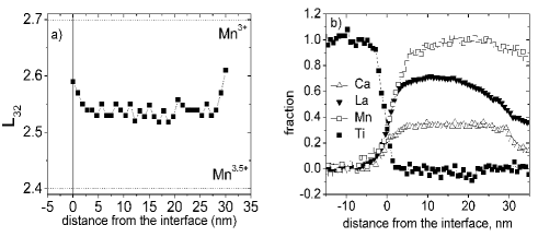
We discuss these findings below, but the conclusion from this paragraph is that we observe a slightly higher (0.1 ) Mn valence at the interface, which relaxes to the bulk value in 2 to 5 nm, and which is not caused by either elemental segregation or by strain.
IV Transport properties
IV.0.1 Films on flat STO
We measured the - characteristics in a temperature range of 20 - 300 K for films with varying thicknesses between 6 - 20 nm, which were linear, except in a small range around the transition, where weak non-linearities were found. In Fig.7 we show the temperature dependent resistance R(T) for three LCMO films grown on flat STO, as determined at an applied current I of 0.1 A.

The films show a clear metal-insulator transition accompanied by a resistance drop of three orders of magnitude. All films show typical CMR effect, a reduction in resistance of a few orders of magnitude upon application of a 5 T magnetic field. For L(20) the transition temperature TMI, which corresponds to the maximum resistance value, is 170 K, which occurs approximately 100 K below TMI for bulk LCMO. TMI is further reduced when the film becomes very thin, L(6) shows the transition at TMI = 110 K, which is 60 K below TMI for L(20).

The dependence on film thickness of TMI is shown in Fig.8. For films grown on flat STO the metal-insulator transition is steadily shifted to lower temperature as the film thickness is reduced. However, the film L(10) (indicated by in Fig.8) grown on flat STO deviated from this trend. This result together with the flat Mn valence profile (Fig.4b implies that L(10) may have a deviating epitaxial relation with the substrate. There is a connected observation in the magnetization measurements, which we will discuss beow.
In the paramagnetic state, R(T) is expected to show activated behavior. In Fig.7, we plot log R vs. T (with the T-axis reciprocal to show the 1/T-behavior). A linear fit to the data provides the activation energy (EA) for the polaron hopping process. For most films the high temperature data show activated behavior with EA = 110 - 120 meV (see Table 1), independent of the film thickness. Deviations typically set in around 1.3x TMI (for example see sample L(15) center panel Fig.7). In this respect at least, the thin films do not behave different from bulk material.
IV.0.2 Films on 1∘ misoriented STO
A novel feature of our studies is the investigation of the effect of unit-cell high step edges on the STO substrate surface on the thin film properties. For these films the transport properties were measured in a four-point geometry with the current directed perpendicular to the step edges (see inset Fig.9). Their thickness was determined from HR-TEM micrographs and is 7 and 8 nm (L(7)mis and L(8)mis). R(T) for L(7)mis was measured at = 0.1 A and is shown in Fig. 9, with R(T) of L(6) shown for comparison.

The observed TMI for both films on 1∘ STO is 145 K, so TMI is much less reduced than for films on flat STO (see Fig.8, triangles). However, from the HR-TEM and RSM characterization it is clear that the films on misoriented STO are fully epitaxial across the entire film thickness. The lack of reduction in TMI for films on misoriented STO is step-induced but not due to the loss of epitaxial relation with the substrate. It has been shown before that strain relaxation in these materials may occur in the form of dislocations in the film lippmaa4 . From HR-TEM we did not observe any dislocations in our thin films, however, point defects should still be present and the amount is possibly enhanced by the presence of the steps.
V Magnetic properties
Here we present the magnetization behavior of the as-grown films on flat and misoriented STO substrates. We have not measured the magnetic properties of the films on NGO because the substrate gives a large paramagnetic background due to the presence of the magnetic Nd3+-ion. Typical behavior of the magnetization vs. measured in magnetic fields of Ha = 0, 0.1 T, 1 T is shown in Fig.10a for L(17). The Curie temperature was determined from M vs. T, measured in zero magnetic field and at Ha = 0.1 T, by taking the intercept of the constant high temperature magnetization with the linearly increasing M(T).
 |
 |
When the film thickness is reduced, we observe that TC is also shifted to lower temperature as shown in Fig. 10b, but continues to coincide with the temperature of the metal-insulator transition. However, when TC is extracted from the measurements in Ha = 0.1 T the Curie temperature is found slightly higher, and aapears to flatten of at low thickness. Probably when measured in still higher fields (for example, Ha = 0.3 T as in Ref.aarts98 ) TC would be independent of film thickness. For the measurement in Ha = 1 T we assume that the magnetization is saturated. In the M(T) behavior at 1 T (see Fig. 10a) the magnetization shows a sudden increase below T = 30 K. The relative strength of this upturn increases as the film thickness is reduced but the temperature at which the upturn starts is constant. This feature is not an intrinsic feature of the LCMO thin films. From Fig.11 it becomes clear that the vs. of a bare STO substrate also shows an upturn below T = 30 K. Apparently, at low T a paramagnetic contribution ( = C/T, with C the Curie constant) dominates but disappears into the diamagnetic background above T = 30 K. We surmise that the emergent paramagnetism is due to the presence of impurities and/or defects in the bulk of the substrate.
 |
 |
We have also investigated the field dependent magnetization at T = 10 K, shown for L(20) in Fig.11b. From these results we can extract the coercive field and the value for the saturation magnetization (Ms) as function of film thickness. The coercive field varies between +/-6 and +/- 15 mT for the different samples. The magnetization is given in units of B per Mn-ion and can be described, at high fields, as M = Ms + H (see inset Fig.11b). The plotted data in the main graph is corrected for the diamagnetic and paramagnetic contribution of the STO substrate by subtracting determined at high fields. The values for Ms are determined after correction by taking the value for M at Ha = 1 T. The theoretical saturation magnetization for bulk LCMO would be 3.7 B per Mn-ion. For our films we observe slightly fluctuating values for Ms but always low compared to the expected bulk value. For L(20) in Fig.11 the value is 2.28 /Mn-ion. The lower values indicate that a magnetically dead or weak layer is generally present in our LCMO thin films.
VI Discussion
The first point to discuss is the reduced Mn-valence we find near the film-substrate interface (also observed in La0.7Sr0.3MnO3/STO riedl3 ), which is not caused by oxygen deficiency. Since the film is grown at high temperature, diffusion of Ti4+ into the film could occur. The presence of the Ti4+ introduces a higher charge and as a result the Mn3+/Mn4+ ratio has to increase to compensate. Characterization of the elemental composition (see Fig.5) and experiments reported by others samet3 show that interdiffusion does not occur beyond a few atomic planes. The EELS analysis of the elemental composition show that in general the films have a composition close to that of the sputtering target, making it likely that the deviating Mn-valence is not associated with cation segregation. Since films grown on NGO show similar Mn-valence profiles the reduction appears to depend on the epitaxial relation between film and substrate but not on epitaxial strain. We suggest that the Mn-valence at the interface is affected by the termination of the substrate. In the case of STO substrates the termination can be Sr2+O2- or Ti4+O, both terminations are neutral. The manganite growth can start with either a [(La0.7Ca0.3)O]0.7+ layer (LaO has charge 1+ and CaO is neutral) or a MnO2 layer which can have charge 1- or be neutral depending on the Mn-valence state. A charge mismatch could therefore arise (Madelung potential) across the LCMO-STO interface.
| Sample | d | ain | aout | TMI | TC | EA | Ms | ddead |
|---|---|---|---|---|---|---|---|---|
| nm | () | () | (K) | (K) | (meV) | (B/Mn) | nm | |
| L(20) | 20 | 3.90 | 3.8113 | 170 | 160 | 109 | 2.28 | 7.6 |
| L(17) | 17 | 3.91 | 3.8135 | 150 | 148 | 114 | 2.89 | 3.7 |
| L(15) | 15 | 3.90 | 3.8097 | 130 | 150 | 115 | 1.96 | 7.0 |
| L(10) | 10.3 | 3.90 | 3.796 | 150 | 170 | 114 | 3.50 | 0.5 |
| L(6) | 6.4 | 3.91 | 3.7979 | 110 | 100 | 115 | 3.30 | 0.7 |
| L(8)mis | 8 | - | - | 145 | 135 | 119 | 2.41 | 2.8 |
| L(7)mis | 7 | 3.90 | 3.7911 | 145 | 131 | 116 | 2.22 | 2.8 |
| L(30)NGO | 30 | - | - | 285 | - | - | - | - |
| L(10)NGO | 10 | - | - | 220 | - | - | - | - |
The reduction of the Mn-valence at the interface shows that growth starts with the
[(La0.7Ca0.3)O]0.7+ layer and that the interface polarization leads
to a charge compensation layer with varying thickness (2 - 5 nm); the variation
could be caused by different TiO2/SrO termination ratios of the substrate
surfaces. This also explains the absence of Mn-valence deviations for films on (110)
STO, as reported by Estradé et al fontcuberta3 . The termination layer of
(110) STO is either Sr2+Ti4+O2- (total charge: 4+) or O. The
first layer of the film would be either La3+Mn3+O2- or
Ca2+Mn4+O2-, which both have a total charge of 4+, or O. The
result is that LCMO (110) grown on STO (110) would not have a charge mismatch
between film and substrate and therefore does not show a Mn-valence reduction at the
substrate interface. The similar Mn-valence profiles in films on NGO substrates are
explained in the same way. We use NGO (100) (pseudocubic notation ngo4 ) which
has either Nd3+O2- or Ga3+O termination layers. The
LCMO(001) film will start the growth with a layer with charge (1-x) (x is the
Ca-doping) as described above. The resulting Madelung potential again leads to the
observed Mn-valence profiles. The only sample for which the Mn-valence reduction is
absent (sample L(10)) possibly shows a deviating film orientation w.r.t. the STO
substrate. It is not a priori clear why there is no charge mismatch for this sample
since the STO would be neutral and the first film layer should still have a charge.
One could imagine that the growth started with a CaMnO3 layer for which the
charge mismatch with the substrate would indeed be equal to 0. The resolution of the
EELS measurement to determine elemental composition would be insufficient to detect
such a small Ca-segregation at the STO interface. We were unable to further
investigate this effect since the absence of the compensation layer was only found
once and is not a general feature of the LCMO thin films. Furthermore, we have
observed that the presence of unit-cell high steps on the STO surface do not
significantly influence the microstructure, the Mn-valence profile or the strain
state of the film.
Next we couple this finding an interface induced Mn valence profile to the other
measured properties, summarized in Table 1. For films on flat STO,
TMI and TC coincide, decrease with decreasing thickness to a final value
around 110 K at a thickness below 10 nm. This agrees very nicely with the data
presented by Bibes et al. bibes01 on similar strained films and
confirms once more the effect of strain on TMI. It is tempting to also connect
our finding of a valence change to their conclusion from NMR data, that a
non-ferromagnetic insulating (NFI) phase exists, at least partly, in a region up to
5 nm from the interface. On the other hand, our thinnest films show an almost full
saturation magnetization in 1 T. This suggest that antiferromagnetic interactions
are significant in the valence-changing layer, but that they are still easily
brought to saturation.
The films with thicknesses of 15 nm and 20 nm show a much lower saturation
magnetization (even in 1 T) than might be expected. Since the valence-changing layer
does not seem to play a role here, this appears to be due to growth-induced defects,
again antiferromagnetic in nature, but now not easily saturated. This is a similar
conclusion as was reached by us before (aarts98 , but in contrast to e.g.
Ref.bibes01 , and appears to depend on the exact growth conditions of the
films. Interestingly, the films on miscut substrates, where relaxation has set in
more strongly, also show low values for . This reinforces the argument that the
step edges lead to disorder in the in the form of local defects lippmaa4 ),
which then also enhances TMI.
VII Conclusion
In this paper we have shown that a layer with lower Mn valence is present close to the interface between a film of La0.7Ca0.3MnO3 and a SrTiO3 or NdGaO3 substrate. It presence is not related to strain but, as we argue, the result of charge compensation. Magnetically we find reduced values for the saturation magnetization for the strained films, but the apparent lack of magnetic moment cannot be exclusively ascribed to the presence of the charge compensation layer. The introduction of step edges onto the SrTiO3 surface leads to a metal-insulator transition temperature TMI which is less reduced than expected from the thickness of the film, which we argue to be due to additional disorder in the form of local defects.
VIII Acknowledgements
We thank I. Komissarov for discussions, and J.A. Boschker (University of Twente) for performing the RSM measurements. This work was part of the research program of the Stichting voor Fundamenteel Onderzoek der Materie (FOM), which is financially supported by NWO.
References
- (1) Y. Tokura, Rep. Prog. Phys. 69 797 (2006); see also Y. Tokura, ’Colossal Magnetoresistive Oxides’, Gordon and Breach Science Publishers (2000).
- (2) E. Dagotto, S. Yunoki, C. Sen, G. Alvarez and A. Moreo, J. Phys.: Condens. Matter bf 20 434224 (2008); see also E. Dagotto, ’Nanoscale phase separation and Colossal Mgnetoresistance’, Springer Series in Solid-State Sciences 136 (2003).
- (3) M. B. Salamon, Rev. Mod. Phys. 73, 583 (2001).
- (4) J.W. Lynn, D. N. Argyriou, Y. Ren, Y. Chen, Y. M. Mukovskii, and D. A. Shulyatev, Phys. Rev. B 76, 014437 (2007).
- (5) J. Aarts, S. Freisem, and R. Hendrikx, and H.W. Zandbergen, Appl. Phys. Lett. 72, 2975 (1998).
- (6) K. Dörr, J. Phys. D: Appl. Phys. 39, R125 R150 (2006).
- (7) M. Bibes, Ll. Balcells, S. Valencia, J. Fontcuberta, M. Wojcik, E. Jedryka, and S. Nadolski, Phys. Rev. Lett. 87, 067210 (2001).
- (8) Z. Q. Yang, R. Hendrikx, J. Aarts, Y. L. Qin and H. W. Zandbergen, Phys. Rev. B 70, 174111 (2004).
- (9) A. Ohtomo and H. Y. Hwang, Nature 427, 423 (2007).
- (10) C. Beekman, J. Zaanen and J. Aarts Phys. Rev. Lett. submitted
- (11) C. Zener, Phys. Rev. 82, 403 (1951)
- (12) A. Machida, M. Itoh, Y. Moritomo, S. Mori, N. Yamamoto ,K. Ohoyama,and A. Nakamura, Physica B 281 282, 524 (2000)
- (13) Y. Tokura and Y.Tomioka, C, J Mag. Mag. Mat. 200, 1 (1999)
- (14) H.Y. Hwang, T.T.M. Palstra, S.-W. Cheong, and B. Batlogg, Phys. Rev. B, 52, 15046 (1995) 39, R125 (2006)
- (15) The pseudocubic lattice parameters (in-plane) and (out-of-plane) as determined from Reciprocal Space Mapping are shown in Table 1.
- (16) Z.Q. Yang, R. Hendrikx, J. Aarts, Y.L. Qin and H.W. Zandbergen, Phys. Rev. B, 70, 174111 (2004)
- (17) Specimen thickness should not be confused with the film thickness.
- (18) Gianluigi et al., J. Microscopy, 180, 211 (1995)
- (19) K. Terai, M. Lippmaa, P. Ahmet and T. Chikyow, T. Fujii, H. Koinuma, and M. Kawasaki, Appl. Phys. Lett. 80, 4437 (2002)
- (20) T. Riedl, T. Gemmin, K. Drr, M. Luysberg, and K. Wetzig, Microsc. Microanal. 15, 213 (2009)
- (21) L. Samet, D. Imhoff, J.-L. Maurice, J.-P. Contour, A. Gloter, T. Manoubi, A. Fert, and C. Colliex, Eur. Phys. J. B. 94, 179 (2003)
- (22) S. Estradé, J. Arbiol, F.Peiró, I.C. Infante, F. Sánchez, J. Fontcuberta, F. de la Peña, M. Walls, and C. Colliex, Appl. Phys. Lett. 93, 112505 (2008)
- (23) Note that different orientations of the NGO substrate lead to different strain states in the film. Here we use NGO (100), cubic notation, which is (110) in orthorhombic notation.