Polarized light emission from individual incandescent carbon nanotubes
Abstract
We fabricate nanoscale lamps which have a filament consisting of a single multiwalled carbon nanotube. After determining the nanotube geometry with a transmission electron microscope, we use Joule heating to bring the filament to incandescence, with peak temperatures in excess of 2000 K. We image the thermal light in both polarizations simultaneously as a function of wavelength and input electrical power. The observed degree of polarization is typically of the order of 75%, a magnitude predicted by a Mie model of the filament that assigns graphene’s optical conductance to each nanotube wall.
pacs:
78.67.Ch, 44.40.+a, 77.22.Ej, 42.25.FxUnderstanding the optical properties of nanoscopic objects remains an outstanding problem in physics. An object’s geometric and electronic structures, which at the nanoscale are interrelated, determine these properties completely. The polarization of light absorbed, emitted, or scattered by an object reports on both, and can reveal information not otherwise available optically, Bohren and Huffman (1983) e.g., the axis of symmetry of an unresolved emitter. Thus polarization provides a handle on understanding the structures key for manipulating and controlling electromagnetic fields at the nanoscale.Bharadwaj et al. (2009)
Carbon nanotubes are theoretically tractable, nontrivial emitters available in a wide array of morphologies, making them ideal test objects for a study comparing structure with polarization. From a size standpoint the two limiting cases have been extensively investigated. Previously polarization-dependent absorption, emission, or reflection has been reported from macroscopic carbon nanotube aggregates such as films,Islam et al. (2004); Murakami et al. (2005) fibers, Hwang et al. (2000) bundles, Li et al. (2003) and arrays. Wang et al. (2004); Cubukcu et al. (2009) Individual single-walled carbon nanotubes (SWCNTs) have also shown polarization effects in their emission, Hartschuh et al. (2003); Lefebvre et al. (2004); Mann et al. (2007); Moritsubo et al. (2010) scattering, Jorio et al. (2002); Sfeir et al. (2004); Joh et al. (2010) and absorption. Lefebvre et al. (2004); Berciaud et al. (2007)
As a class of material, individual multiwalled carbon nanotubes (MWCNTs) straddle the boundary between the macroscopic and molecular limits. A many-layered MWCNT has a dielectric response like that of bulk graphite, while decreasing the number of layers to the limiting value of one produces a SWCNT - essentially a large molecule with discrete spectral features. Polarization effects in the challenging intermediate regime represented by individual MWCNTs have not been explored previously.
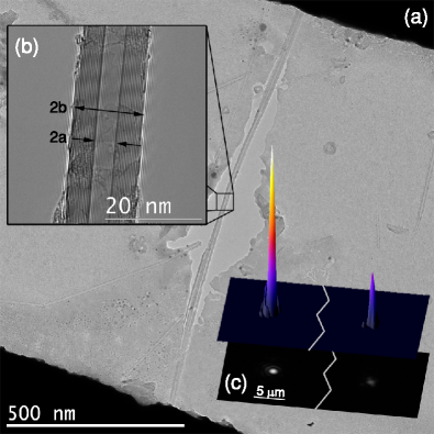
We present here a study of polarized light emission from individual incandescent MWCNTs, where the emitter peak temperatures are in excess of 2000 K. Our data quantify the polarization and its wavelength dependence throughout the visible into the near infrared (450–1100 nm), with sub-wavelength resolution of the emitter in both polarizations simultaneously. Also unique, however, is that each individual emitter is imaged with atomic resolution in a transmission electron microscope (TEM). These images fully characterize the source, providing precise determinations of the nanotube lengths, radii, and numbers of walls. The MWCNTs observed have 10-20 walls, core radii of nm, and outer radii of 7–9 nm, putting them in the regime where molecular spectral features are not expected and the classical theory provides a reasonable first approximation. Thus we analyze the observed degree of optical polarization () using the Mie model of a small, conducting tube and the structural information provided by the TEM.

The nanotube lamp fabrication process and the basics of the optical system have been described previously.Fan et al. (2009) The two-terminal devices have an active element consisting of an arc-discharge grown MWCNT suspended on an electron-transparent Si3N4 membrane window in a 2 mm2 mm mm silicon chip. After imaging a device in the TEM, we load it into a high-vacuum chamber for optical characterization (see Fig. 1) and apply an increasing bias voltage over a period of some minutes. With sufficient applied power the membrane neighboring the midpoint of the device disintegrates, as indicated by a decrease in the current at constant voltage accompanied by a 10%–20% increase in device brightness. Both effects are attributed to the improved thermal isolation, and therefore higher temperature, of the center section of the nanotube. Taking the membrane disintegration to initiate near the dissociation temperature of Si3N4, we adopt 2000 K as a conservative lower bound on the central temperature of the device at that applied bias voltage.Begtrup et al. (2007) After the optical experiments have been completed the membrane disintegration is confirmed in the TEM (see Fig. 2). The Si3N4 membrane is a thin, excellent insulator with a correspondingly tiny () emissivity in the visible; we have not seen evidence of light emission from any source other than the nanotube itself.

Simultaneous imaging of the nanotube in both polarizations is achieved by placing a Wollaston prism in the optical microscope’s infinity space (see Fig. 1). The quartz prism introduces an angular displacement of between the two orthogonal polarizations, which creates an effective position displacement of 7 mm (70 m) in the image (object) plane. Both single polarization images of the radiating nanotube are easily captured by the mm2 CCD sensor. With the prism mounted on a rotation stage and an array of 10 nm bandpass filters we image both polarizations simultaneously as a function of power, wavelength, and prism angle.
We define parallel () and perpendicular () light polarizations by the prism orientation that maximizes the contrast in a single image, and calculate the of the nanotube’s emission with Bohren and Huffman (1983)
| (1) |
To most closely approximate an isothermal field of view, is taken to be the photon count rate in the spot’s brightest pixel, an effective area of ( nm)2. depends on , the emitting area , the temperature via the Planck factor, and the optical system efficiency, Fan et al. (2009) but these common factors cancel in the , leaving
| (2) |
Here is the absorption efficiency, or equivalently emissivity, Bohren and Huffman (1983); Schuller et al. (2009) of the nanotube in the specified polarization.
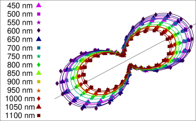
Figure 3 shows representative data from the nanotube device in Fig. 2, plotted as a polar function of intensity and prism angle. The phase offset gives the angle of maximum polarization, which matches the orientation of the nanotube’s long axis as determined by the relative orientations of the optical and TEM images. Fan et al. (2009) A 2D Gaussian fit to the nanotube’s optical image alone also yields a major axis consistent with the other two determinations. The for this device is seen to vary with wavelength, showing a gentle peak near nm.

Polarization effects in the absorption or emission of light from carbon nanotubes, especially SWCNTs, have been treated theoretically. Milosevic et al. (2003); Saito et al. (2004); Goupalov (2005) Emission perpendicular to the nanotube axis is thought to be strongly suppressed by the “depolarization effect,” Ajiki and Ando (1994); Benedict et al. (1995); Marinopoulos et al. (2003) where charge induced on the nanotube walls cancels the internal electric field. Ajiki and Ando (1994); Saito et al. (2004) However, we are unaware of theory predicting the expected from a single MWCNT.
For a model with which we can compare our experimental results, we turn to classical Mie theory, which has found success in predicting the scattering and absorption of gold nanoparticlesvan Dijk et al. (2006) and metallic dust grainsRosenberg et al. (2008). We model the nanotube as an infinitely long, cylindrical tube with inner radius and outer radius . The problem of scattering and absorption by a solid infinite right circular cylinder has been treated by Bohren and Huffman Bohren and Huffman (1983). Their derivation considers a plane wave of wavevector incident on the cylinder at an angle measured from the tube axis, and solves for the extinction and scattering by calculating the scattered wave and invoking conservation of energy. The scattered fields are described with an infinite series of coefficients and that weight the solutions to the wave equation in cylindrical coordinates. Requiring continuity of the electromagnetic fields on the surface fixes the series coefficients. Modifying this derivation for the tubular case, we find extinction and scattering efficiencies
| (3) |
for an incident wave polarized perpendicular to the tube axis. Similar relations hold for the parallel extinction and scattering efficiencies and , which are found by making the substitutions and in the relations for and . For a narrow () tube in vacuum, the and coefficients are, to the lowest nontrivial order in and ,
| (4) |
The tube’s complex index of refraction is assumed to satisfy here. The absorption efficiency , since is negligible for . In terms of the dielectric constant ,
| (5) |
As expected, is independent of incidence angle, and at (incident wave parallel to the tube axis), the absorption efficiencies are equal.
The dielectric constant can be written in the form , where the conductivity is in general complex and is the impedance of free space. To complete the model, we approximate each nanotube wallMurakami et al. (2005); Skulason et al. (2010) as having the frequency-independent, two-dimensional (2D) optical conductance per square expected for a graphene sheetAndo et al. (2002); Gusynin et al. (2006); Mecklenburg et al. (2010) ( is the fine-structure constant). We define an effective three-dimensional (3D) conductivity , where is the thickness, is the number of walls, and nm is their spacing. The absorption coefficients are then determined in terms of the dimensionless quantity .
Our calculations are based on the expressions (5), but to elucidate their structure we consider the zero thickness limit where . In this limit, the prior assumption is equivalent to and Eq. 5 reduces to
| (6) |
Equation (6) gives a between for small and unity for large at normal incidence ). This trend with tube radius is consistent with data showing that SWCNTs have greater s than our MWCNTs, with sub-nanometer diameter SWCNTs exhibiting the greatest s. Hartschuh et al. (2003); Lefebvre et al. (2004); Mann et al. (2007) A quantitative treatment of SWCNTs is beyond the scope of this theory, since we do not account for resonance or selection rule effects. Ajiki and Ando (1994); Benedict et al. (1995); Marinopoulos et al. (2003); Milosevic et al. (2003); Saito et al. (2004); Goupalov (2005) Generally Eq. (5) gives smaller s for large tubes with large cores (), and s largely independent of for small cores ().

Returning to (5), we integrate the absorption efficiencies over the NA to find the observed ,
| (7) |
where for our NA.
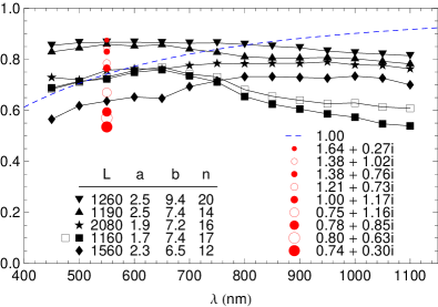
Figure 4 summarizes the data for five different nanotube devices. Also shown is the prediction of Eq. (7) for nanotube radii as determined by TEM and a graphene-like optical conductance of per wall. The prediction varies little for the range of ’s and ’s explored, but is sensitive to the conductance; taking other values from the literature can move the sufficiently to encompass all of the data. Thus we find that Mie theory and optical constants characteristic of multilayer graphene reproduce the observed magnitude of the .
Beyond the evident coarse agreement with the Mie model, the data raise some questions. First, it is not yet clear how to explain the observed variance between devices with the detailed geometric information made available by the TEM images. Second, for a frequency-independent optical conductivity, Mie theory predicts a that increases with wavelength; much of the data indicate the opposite trend. Furthermore, the is generally observed to decrease with increasing applied bias (or equivalently temperature), with the effect stronger at longer wavelengths. Figure 4 shows a second curve (labeled ), representing a midpoint temperature K cooler, for the device that illustrates this effect most dramatically. At maximum bias these devices are operating at temperatures where optical and zone-boundary phonon modes (V K) are thermally populated; we suggest that the resulting decrease in the electronic mean free path makes the bias electric field less effective in establishing the polarization axis Yao et al. (2000). However, a more comprehensive theoretical picture than our Mie model will be required to capture these effects.
In conclusion, we have structurally characterized individual MWCNTs, brought them to incandescence, and measured their polarized light emission. Assuming optical conductances characteristic of graphene, a simple model based on classical Mie theory predicts the magnitude of the observed degree of polarization of . A complete explanation of the variations around this value that depend on wavelength, device configuration, and device temperature requires a more sophisticated model. Future research on MWCNTs, especially those with fewer walls, will further probe the classical-quantum transition regime and advance our understanding of nanoscale optical devices.
This project is supported by NSF CAREER Grant No. 0748880. All TEM work was performed at the Electron Imaging Center for NanoMachines at UCLA.
References
- Bohren and Huffman (1983) C. F. Bohren and D. R. Huffman, Absorption and scattering of light by small particles (Wiley, New York, 1983).
- Bharadwaj et al. (2009) P. Bharadwaj, B. Deutsch, and L. Novotny, Advances in Optics and Photonics 1, 438 (2009).
- Islam et al. (2004) M. F. Islam, D. E. Milkie, C. L. Kane, A. G. Yodh, and J. M. Kikkawa, Physical Review Letters 93, 037404 (2004).
- Murakami et al. (2005) Y. Murakami, E. Einarsson, T. Edamura, and S. Maruyama, Physical Review Letters 94, 087402 (2005).
- Hwang et al. (2000) J. Hwang, H. H. Gommans, A. Ugawa, H. Tashiro, R. Haggenmueller, K. I. Winey, J. E. Fischer, D. B. Tanner, and A. G. Rinzler, Physical Review B 62, R13310 (2000).
- Li et al. (2003) P. Li, K. L. Jiang, M. Liu, Q. Q. Li, S. S. Fan, and J. L. Sun, Applied Physics Letters 82, 1763 (2003).
- Wang et al. (2004) Y. Wang, K. Kempa, B. Kimball, J. B. Carlson, G. Benham, W. Z. Li, T. Kempa, J. Rybczynski, A. Herczynski, and Z. F. Ren, Applied Physics Letters 85, 2607 (2004).
- Cubukcu et al. (2009) E. Cubukcu, F. Degirmenci, C. Kocabas, M. A. Zimmler, J. A. Rogers, and F. Capasso, Proceedings of the National Academy of Sciences of the United States of America 106, 2495 (2009).
- Hartschuh et al. (2003) A. Hartschuh, H. N. Pedrosa, L. Novotny, and T. D. Krauss, Science 301, 1354 (2003).
- Lefebvre et al. (2004) J. Lefebvre, J. M. Fraser, P. Finnie, and Y. Homma, Physical Review B 69, 075403 (2004).
- Mann et al. (2007) D. Mann, Y. K. Kato, A. Kinkhabwala, E. Pop, J. Cao, X. R. Wang, L. Zhang, Q. Wang, J. Guo, and H. J. Dai, Nature Nanotechnology 2, 33 (2007).
- Moritsubo et al. (2010) S. Moritsubo, T. Murai, T. Shimada, Y. Murakami, S. Chiashi, S. Maruyama, and Y. K. Kato, Physical Review Letters 104, 247402 (2010).
- Jorio et al. (2002) A. Jorio, A. G. S. Filho, V. W. Brar, A. K. Swan, M. S. Unlu, B. B. Goldberg, A. Righi, J. H. Hafner, C. M. Lieber, R. Saito, G. Dresselhaus, and M. S. Dresselhaus, Physical Review B 65, 121402(R) (2002).
- Sfeir et al. (2004) M. Y. Sfeir, F. Wang, L. M. Huang, C. C. Chuang, J. Hone, S. P. O’Brien, T. F. Heinz, and L. E. Brus, Science 306, 1540 (2004).
- Joh et al. (2010) D. Y. Joh, J. Kinder, L. H. Herman, S. Y. Ju, M. A. Segal, J. N. Johnson, G. K. L. Chan, and J. Park, Nature Nanotechnology 6, 51 (2010).
- Berciaud et al. (2007) S. Berciaud, L. Cognet, P. Poulin, R. B. Weisman, and B. Lounis, Nano Letters 7, 1203 (2007).
- Fan et al. (2009) Y. W. Fan, S. B. Singer, R. Bergstrom, and B. C. Regan, Physical Review Letters 102, 187402 (2009).
- Begtrup et al. (2007) G. E. Begtrup, K. G. Ray, B. M. Kessler, T. D. Yuzvinsky, H. Garcia, and A. Zettl, Physical Review Letters 99, 155901 (2007).
- Schuller et al. (2009) J. A. Schuller, T. Taubner, and M. L. Brongersma, Nature Photonics 3, 658 (2009).
- Milosevic et al. (2003) I. Milosevic, T. Vukovic, S. Dmitrovic, and M. Damnjanovic, Physical Review B 67, 165418 (2003).
- Saito et al. (2004) R. Saito, A. Gruneis, G. G. Samsonidze, G. Dresselhaus, M. S. Dresselhaus, A. Jorio, L. G. Cancado, M. A. Pimenta, and A. G. Souza, Applied Physics a-Materials Science and Processing 78, 1099 (2004).
- Goupalov (2005) S. V. Goupalov, Physical Review B 72, 195403 (2005).
- Ajiki and Ando (1994) H. Ajiki and T. Ando, Physica B 201, 349 (1994).
- Benedict et al. (1995) L. X. Benedict, S. G. Louie, and M. L. Cohen, Physical Review B 52, 8541 (1995).
- Marinopoulos et al. (2003) A. G. Marinopoulos, L. Reining, A. Rubio, and N. Vast, Physical Review Letters 91, 046402 (2003).
- van Dijk et al. (2006) M. A. van Dijk, A. L. Tchebotareva, M. Orrit, M. Lippitz, S. Berciaud, D. Lasne, L. Cognet, and B. Lounis, Physical Chemistry Chemical Physics 8, 3486 (2006).
- Rosenberg et al. (2008) M. Rosenberg, R. D. Smirnov, and A. Y. Pigarov, Journal of Physics D-Applied Physics 41, 015202 (2008).
- Skulason et al. (2010) H. S. Skulason, P. E. Gaskell, and T. Szkopek, Nanotechnology 21, 1099 (2010).
- Ando et al. (2002) T. Ando, Y. S. Zheng, and H. Suzuura, Journal of the Physical Society of Japan 71, 1318 (2002).
- Gusynin et al. (2006) V. P. Gusynin, S. G. Sharapov, and J. P. Carbotte, Physical Review Letters 96, 256802 (2006).
- Mecklenburg et al. (2010) M. Mecklenburg, J. Woo, and B. C. Regan, Physical Review B 81, 245401 (2010).
- Yao et al. (2000) Z. Yao, C. L. Kane, and C. Dekker, Physical Review Letters 84, 2941 (2000).