∎
INVITED PAPER††thanks: The UBC authors acknowledge support from the National Science and Engineering Research Council and the British Columbia Innovation Council.
Abstract
A multiple quantum well (MQW) transistor vertical-cavity surface-emitting laser (T-VCSEL) is designed and numerically modeled. The important physical models and parameters are discussed and validated by modeling a conventional VCSEL and comparing the results with the experiment. The quantum capture/escape process is simulated using the quantum-trap model and shows a significant effect on the electrical output of the T-VCSEL. The parameters extracted from the numerical simulation are imported into the analytic modeling to predict the frequency response and simulate the large-signal modulation up to 40 Gbps.
Keywords:
Transistor laser VCSEL Numerical modeling Quantum-trap model Direct modulation1 Introduction
While most semiconductor lasers are diode structures, transistor lasers TL are attracting much attention for their potential for high-frequency operation Microwave and unique carrier dynamics CB . Different from monolithically integrating a transistor and a laser diode, either in-plane MonoInteg or vertically VertiInteg , where the transistor performs as the electrical driver of the laser, transistor lasers use the base recombination to provide stimulated emission. Early works on transistor lasers include a conceptual proposal of quantum well (QW) transistor lasers QW_LT_old and experimental demonstration of a laser transistor LaserTransistor that could function as a laser and a transistor in separate states. The recently developed QW transistor laser TL has two independent control signals and can simultaneously output an electrical signal and an optical signal. This makes possible a simpler method of implementing feedback operation TVCSEL_feedback , a unique voltage-controlled mode TXVCSEL , and a new optoelectronic integration scheme. Compared with edge-emitting lasers, vertical-cavity surface-emitting lasers (VCSELs) have many attractive features VCSEL_advances such as low power consumption, large-scale 2D array fabrication, on-wafer testing, single longitudinal mode operation, and a narrow circular beam. Integrating a heterojunction bipolar transistor (HBT) structure into a vertical cavity, transistor VCSELs (T-VCSELs) TXVCSEL could combine the optoelectronic properties of the transistor laser with the advantages of VCSELs.
In this work, we design and model a multiple QW (MQW) T-VCSEL self-consistently. The important parameters are calibrated by matching the simulation to the experiment of a conventional VCSEL. We link the numerical model with our previously developed analytic model Analytical , using the quantum-trap model, to predict its frequency response and large-signal-modulation performance under different transistor bias configurations.
2 Design
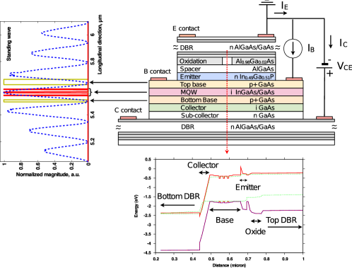
The T-VCSEL, as shown in Fig. 1, has an Npn In0.49Ga0.51P/GaAs HBT structure. The bottom and top distributed Bragg reflectors (DBRs) consist of 36 pairs and 24 pairs of Al0.85Ga0.15As/GaAs, respectively. The base region plays a critical role in determinating the electrical and optical performance of a transistor laser TL_OE . In this design, we use an asymmetric base doping profile where the whole base region is composed of (from bottom to top) a 15 nm heavily doped () layer, a 30 nm doping grading layer, three intrinsic In0.17Ga0.83As/GaAs QWs, another 30 nm doping grading layer, and a 40 nm heavily doped () base-contact layer. The heavily doped layers are aligned with the nodes of the longitudinal standing wave (as shown in the inset of Fig. 1) in the vertical cavity to reduce the optical absorption. A -diameter oxide aperture is used for electrical and optical confinement.
3 Numerical modeling
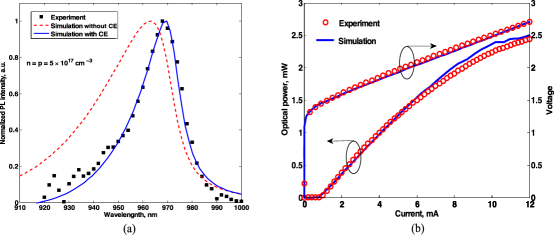
To investigate the physics and performance of the T-VCSEL, we have used PICS3D, an advanced numerical simulation software Crosslight , that solves the electrical and optical models numerically and self-consistently. The carrier transport is described based on the classic drift-diffusion model Semiconductor_physics , with the thermionic-emission model Semiconductor_physics used at the heterojunctions. Lateral optical modes are calculated by the effective-index method EEM . In the strained QWs, the conduction bands are assumed to be parabolic, and the valence bands are calculated by the 66 kp method for the valance-band mixing kp_method . The important parameters for QWs are carefully calibrated to match the measured photoluminescence (PL): while the reported values of the band-edge offset for strained InGaAs/GaAs QWs have a big spread III-V_Band , it is assumed to be Band_offset_InGaAs ; a scattering time of 85 fs is used in Lorentz broadening; bandgap renormalization is considered as a function of the local carrier density of electrons (n) and holes (p): . With Coulomb enhancement ManyBody included in calculating the optical gain and spontaneous emission, good agreement is achieved for the PL spectrum, as shown in Fig. 2 (a). The optical loss due to the free-carrier and intervalence-band absorption is calculated by with and for the passive layers Model_GaAs_detector and and for the QWs Model_980_pump . The Auger recombination is calculated by by assuming that the CHHS Auger process dominates Auger_InP . The Auger coefficient is assumed to be for the passive layers Auger_GaAs and for the QWs Model_980_VCSEL . To verify the models and determine the material parameters, we have fabricated and simulated a conventional oxide-confined VCSEL that has the same QW structure as the designed T-VCSEL, taking self-heating into consideration. The power-law model Model_heterostructure is used for AlGaAs thermal conductivity. The thermal conductivity () of the AlGaAs/GaAs DBRs as a function of temperature () is given by where is used to describe the effect of phonon scattering Thermal_DBR due to the DBR interfaces and is tuned to be 0.5 for the lateral direction and 0.4 for the vertical direction. The carrier mobility is also affected by the phonon scattering and 75-percent reduction of the average mobility of AlGaAs and GaAs for the DBRs gives a good agreement with measured LIV curves, as demonstrated in Fig. 2 (b). Thermal effect is not considered in the T-VCSEL modeling.
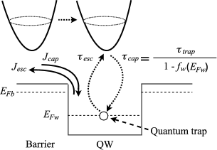
The QW capture/escape process has a significant influence on the frequency response of QW diode lasers Transiport_review as well as of transistor lasers Analytical . In this work, this process is described by a quantum-trap model in which the QWs are treated as carrier traps with trapping rates determined by phonon scattering theory q_transport . The capture current () and escape current () of electrons (the minority carriers in the base) are given by
| (1) | |||||
| (2) |
where , , and are capture time, trapping time, and escape time, respectively; is the QW thickness; , , and represent carrier density, quasi-Fermi level, and occupancy, respectively, with the subscripts indicating “well” and “barrier”. From Eq. 1 we see that can be determined from based on the Fermi-Dirac distribution. In addition, can be calculated by in the quasi-equilibrium condition in which is assumed to be equal to and hence . Therefore, from Eq. 1 and 2 we can find :
| (3) |
4 DC performance
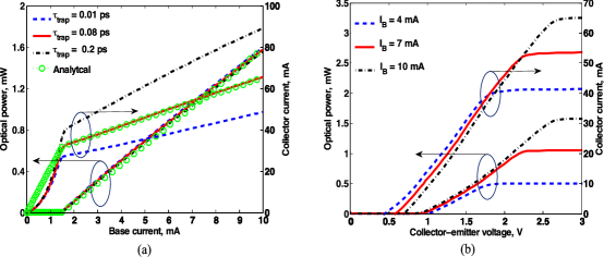
In the active state of transistor operation, the emitter-base junction is forward biased and the collector-base junction is reversed biased, which is evident in the band diagram (Fig. 1). Fig. 4 (a) shows the simulated electrical output (collector current ) and optical output as functions of the input signal (base current ). The electrical gain drops suddenly (from 21.2 to 3.9 for ) at threshold (1.5 mA) due to the stimulated emission. We notice that while the L-I curves are almost unaffected by the trapping time, the collector current is very sensitive to the capture/escape process. This is because the stimulated emission is dominated by the hole current injected into the base, however, the electrons can either be recombined with the holes in the optical collector (i.e. QWs) or leave the transistor via the electrical collector. In the following simulation, we use that corresponds to a capture time of at threshold Analytical . Due to the three-port operation and device geometry, the optical power of a T-VCSEL is controlled both by the base current (which is determined by the base recombinations) and the collector-emitter voltage (that controls the effective current injected into the optical cavity) TXVCSEL . As shown in Fig. 4 (b), the optical output follows the same trend as the collector current, which means that we can potentially monitor the optical performance by the electrical output. This voltage-controlled operation may find applications in optical communications and signal processing TunnelTL_mixing .
5 Modulation response
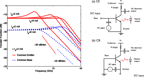
Several analytic models, including the charge-control model Microwave and the carrier-transport model that considers the quantum capture/escape process Analytical have been developed. These models have been used to investigate the transistor lasers’ frequency response Microwave ; Analytical and large-signal modulation Zhang2009 ; Mizuki_CLEO2010 . Here we use the model developed in Analytical and solve the equations numerically by the finite difference method taflove . Using the parameters extracted from the numerical modeling by PICS3D, the analytic model matches well the DC results from the numerical simulation, as shown in Fig. 4 (a). Knowing the minority carrier distribution, we can study the T-VCSEL’s modulation behavior under different configurations, i.e., common-emitter (CE) or common-base (CB). Fig. 5 shows the frequency responses of the T-VCSEL in both configurations. We can see that while the CE configuration has the same response as normal laser diodes (as shown in Analytical ), the CB configuration demonstrates a -40 dB/dec decay after relaxation oscillation and a bandwidth enhancement, albeit, a reduction of the DC response due to the transistor current gain Analytical . For the large-signal modulation, we report the eye-diagrams for both configurations. Figs. 6 (a)-(c) show the eye-diagrams of the T-VCSEL, in the CB configuration, directly modulated at 10, 20, and 40 Gbps, respectively. Figs. 6 (e)-(f) are for the CE configuration. We can see that while the “eye” of the CE configuration starts closing at 20 Gbps, the CB configuration has an open eye-diagram up to 40 Gbps due to a larger bandwidth.
(a)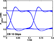 (b)
(b)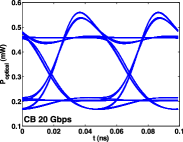 (c)
(c)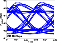 (d)
(d)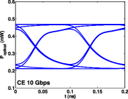 (e)
(e)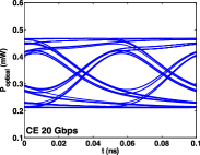 (f)
(f)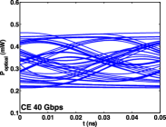
6 Conclusions
We have demonstrated the design and modeling of an InGaAs MQW T-VCSEL, a vertical-cavity laser with an extra electrical output coupled to its optical output. The model has been verified by modeling a conventional VCSEL and matching the simulation results with experiments. It has been shown that the quantum capture/escape process (described by a quantum-trap model in this work) in the base of the T-VCSEL significantly affects its electrical output and, although less important for its optical DC performance, needs to be carefully treated for calculating its optical frequency response as it is highly related to the transistor’s electrical gain. Our simulation has predicted a bandwidth enhancement and better large-signal performance of the T-VCSEL in the CB configuration. With a compact size, large-scale-integration capacity, a high bandwidth, and flexible three-port operation, the T-VCSEL should find novel applications in optical communications, optoelectronic data processing, and optical interconnects.
References
- (1) M. Feng, J. N. Holonyak, G. Walter, and R. Chan, “Room temperature continuous wave operation of a heterojunction bipolar transistor laser,” Appl. Phys. Lett. 87, p. 131103, 2005.
- (2) H. W. Then, M. Feng, and J. N. Holonyak, “Microwave circuit model for the three-port transistor laser,” Appl. Phys. Lett. 107, p. 094509, 2010.
- (3) B. Faraji, W. Shi, D. L. Pulfrey, and L. Chrostowski, “Common-emitter and common-base small-signal operation of the transistor laser,” Appl. Phys. Lett. 93, p. 143503, 2008.
- (4) J. Katz, N. Bar-Chaim, P. C. Chen, S. Margalit, I. Ury, D. Wilt, M. Yust, and A. Yariv, “A monolithic integration of GaAs/GaAlAs bipolar transistor and heterostructure laser,” Appl. Phys. Lett. 37, pp. 211–213, 1980.
- (5) T. R. Chen, K. Utaka, and Y. H. Z. Y. Y. L. A. Yariv, “Vertical integration of an InGaAsP/InP heterojunction bipolar transistor and a double heterostructure laser,” Appl. Phys. Lett. 50, pp. 874–876, 1987.
- (6) F. Jain, C. Chung, R. LaComb, and M. Gokhale, “Resonant tunneling transistor lasers: A new approach to obtain multi-state switching and bistable operation,” Intl. J. Infrared and Millimeter Waves 14, pp. 1311–1322, 1993.
- (7) Y. Mori, J. Shibata, Y. Sasai, H. Serizawa, and T. Kaijiwara, “Operation principle of the InGaAsP/InP laser transistor,” Appl. Phys. Lett. 47, pp. 649–651, 1985.
- (8) B. Faraji, N. A. F. Jaeger, and L. Chrostowski, “Modelling the effect of the feedback on the small signal modulation of the transistor laser,” in 23rd Annual Meeting of the IEEE Photonics Society, p. WX4, (Denver, CO, USA), 11 2010.
- (9) W. Shi, L. Chrostowski, and B. Faraji, “Numerical study of the optical saturation and voltage control of a transistor vertical cavity surface emitting laser,” IEEE Photonics Technology Letters. 20, pp. 2141–2143, 2008.
- (10) I. Koyama, “Recent advances of VCSEL photonics,” IEEE J. Lightwaves 24, pp. 4502–4513, 2006.
- (11) B. Faraji, W. Shi, D. L. Pulfrey, and L. Chrostowski, “Analytical modeling of the transistor laser,” IEEE J. Quantum Electron. 15, pp. 594–603, 2009.
- (12) Z. Duan, W. Shi, L. Chrostowski, X. Huang, N. Zhou, and G. Chai, “Design and epitaxy of 1.5 m InGaAsP-InP mqw material for a transistor laser,” Optics Express 18, pp. 1501–1509, 2010.
- (13) Crosslight Device Simulation Software – A General Description, Crosslight Software Inc., 2005.
- (14) S. M. Sze, Physics of Semiconductor Devices, Wiley-Interscience; 2nd Edition, New York, 1981.
- (15) G. R. Hadley, K. L. Lear, M. E. Warren, K. D. Choquette, J. W. Scott, and S. W. Corzine, “Comprehensive numerical modeling of vertical-cavity surface-emitting lasers,” IEEE J. Quantum Electron. 32, pp. 607–616, 1996.
- (16) S. L. Chuang, “Efficient band structure calculations of strained quantum wells,” Phys. Rev. B 43, 1991.
- (17) I. Vurgaftman and J. R. Meyer, “Band parameters for III-V compound semiconductors and their alloys,” J. Appl. Phys. 89, pp. 5815–5875, 2001.
- (18) V. D. Kulakovskii, T. G. Andersson, and L. V. Butov, “Band edge offset in strained InxGa1-xAs/GaAs quantum wells measured by high-excitation photoluminescence,” Semicond. Sci. Technol. 8, pp. 477–480, 1993.
- (19) C. F. Hsu, J. P. S. Zory, and C.-H. Wu, “Coulomb enhancement in InGaAs-GaAs quantum-well lasers,” IEEE J. Sel. Topics Quantum Electron. 3, 1997.
- (20) J. Piprek, D. Lasaosa, D. Pasquariello, and J. E. Bowers, “Optimization of GaAs amplification photodetectors for 700% quantum efficiency,” IEEE J. Sel. Topics Quantum Electron. 9, pp. 776–782, 2003.
- (21) M. Nawaz and K. Permthammasin, “A design analysis of a GaInP/GaInAs/GaAs-based 980 nm al-free pump laser using self-consistent numerical simulation,” Semicond. Sci. Technol. 16, pp. 877–884, 2001.
- (22) S. Seki, W. W. Lui, and K. Yokoyama Appl. Phys. Lett. 66, pp. 3093–3095, 1995.
- (23) R. K. Ahrenkiel, R. Ellingson, and W. Metzger, “Auger recombination in heavily carbon-doped GaAs,” Appl. Phys. Lett. 78, pp. 1897–1881, 2001.
- (24) Y. Liu, W.-C. Ng, K. D. Choquette, and K. Hess, “Numerical investigation of self-heating effects of oxide-confined vertical-cavity surface-emitting lasers,” IEEE J. Quantum Electron. 41, pp. 15–25, 2005.
- (25) L. A. Coldren and S. W. Corzine, Analysis and simulation of heterostructure devices, Springer-Verlag Wien New York, Austria, 2004.
- (26) J. Piprek, T. Trger, B. Schrter, J. Kolodzey, and C. S. Ih, “Thermal conductivity reduction in GaAs-AlAs distributed bragg reflectors,” IEEE Photon. Technol. Lett. 10, pp. 81–83, 1998.
- (27) R. Nagarajan, “Carrier transport effects in quantum well lasers: an overview,” Opt. Quantum Electron. 26, pp. S647–S666, 1994.
- (28) M. A. Alam, M. S. Hybertsen, R. K. Smith, and G. A. Baraff, “Simulation of semiconductor quantum well lasers,” IEEE T. Electron. Dev. 47, p. 1917, 2000.
- (29) H. W. Then, C. H. Wu, G. Walter, M. Feng, and N. Holonyak, “Electrical-optical signal mixing and multiplication (2 22GHz) with a tunnel junction transistor laser,” Applied Physics Letters 94, p. 101114, 2009.
- (30) L. Zhang and J. P. Leburton, “Modeling of the transient characteristics of heterojunction bipolar transistor lasers,” IEEE Journal of Quantum Electronics 45, pp. 359–366, 2009.
- (31) M. Shirao, N. N. S. Lee, and S. Arai, “Large signal analysis of AlGaInAs/InP laser transistor,” in Conference on Lasers and Electro-Optics, p. CMY7, (San Jose, CA), 2010.
- (32) A. Taflove and S. C. Hagness, Computational electrodynamics: The finite-difference time-domain method, Artech House, 2005.