Underlap Optimization in HFinFET in Presence of Interface Traps
I Introduction
The challenge to scale bulk MOSFET is ever increasing, particularly beyond 22 nm technology node, due to significantly large short channel effects and it gradually becomes essential to get equipped with the alternate technologies to continue CMOS scaling [1]. FinFET is one of the options which provides excellent scalability due to its non-planar structure[2]-[4]. Recently, a hybrid architecture of HEMT [5]-[7] and FinFET, called HFinFET, has been proposed to obtain high performance as well as improved short channel effects [8]. The design relies on the improved on performance from an HEMT-like on operation coupled with good short channel control due to a FinFET-like multi-gate non-planar structure.
The aim of this work is to investigate further scalability of HFinFET using gate to S/D underlap length [9]-[11] as a tuning knob and we show that without much performance degradation, the on-off ratio as well as the subthreshold slope of an HFinFET can be improved significantly for channel length down to nm. We also investigate the effect of channel-gate insulator interfacial traps on device performance. This is very important because the device has III-V channel material and the current technology does not offer an excellent interface with gate dielectric [12]-[14]. Finally, we show that the underlap parameter can be tuned to largely mitigate the interface trap related issues, while meeting the performance projection by ITRS 2009 [1].
II Device Structure and Simulation Method
The top view of the schematic diagram of a HFinFET and its cross section along the dotted line are shown in Fig. 1. The channel (Fin) is of In0.53Ga0.47As sitting on an insulator. The hard mask on the top is thick enough so that the effect of the top gate can be neglected. A barrier layer, having a conduction band offset, is sandwiched between the channel and the hard mask. During on condition, the device electrostatics allows the delta doped layer in the barrier layer to supply carriers to the channel. During off state, these carriers can be pulled out of the channel by the application of appropriate bias at the side gates, separated from the channel by the gate dielectric. This combined effect of HEMT and FinFET allows the device to obtain good on as well as off performance.
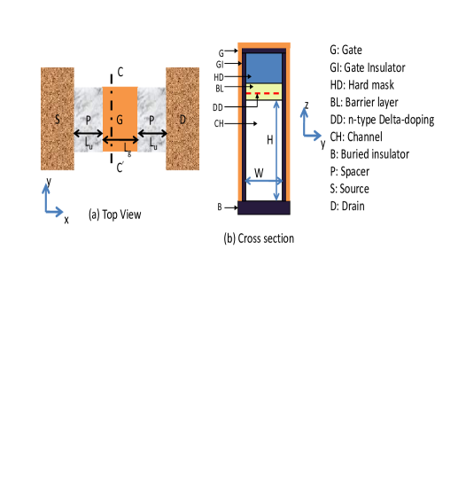
The metal gate work function ensures flatband on condition [15], which, coupled with the low carrier effective mass of the undoped channel, pushes the transistor close to the ballistic limit at shorter channel lengths. We have employed an effective mass based 3-D Poisson-Schrodinger solver coupled with ballistic transport [16]-[20] to simulate the device. More details about the device operation and the simulation method are explained in ref. [8]. In this work, we assume the equivalent oxide thickness (EOT) of the gate dielectric to be nm. Assuming use of high-k dielectric which allows thicker physical oxide thickness [12]-[14], the gate leakage has been assumed to be negligible and has not been taken into consideration in the simulation. The doping of the n-type delta doped layer is assumed to be cm-2, which supply electrons in the channel. We consider the gate length () as nm and nm with three different fin widths: nm, nm and nm. The fin height () is assumed to be nm for all the cases. We assume the supply voltage to be V. To obtain a realistic estimate on the device performance, we assume series source () and drain resistance (), each of which being m. In the following, we use the four performance criteria proposed in [21], namely, (1) intrinsic gate delay (), (2) energy-delay product (), (3) subthreshold slope () and (4) intrinsic gate delay versus on-off ratio, to benchmark the device performance. The performance predictions are compared against ITRS 2009 projections [1] as well as Si planar and non-planar devices of similar gate lengths [3, 21, 22].
III Underlap Optimization
In this work, we assume a symmetric gate-to-source and gate-to-drain underlap (). With an increase in , the drain to source coupling reduces significantly, particularly for a shorter channel, which in turn gets reflected in the off state leakage as well as subthreshold slope of the device. However, at the same time, the underlap increases the series resistance of the channel, degrading the on performance [9]-[11]. The results are shown in Fig. 2 for two different channel lengths (=nm and nm) with a fixed fin width of =7.5nm. In Fig. 2(a), we observe a significant improvement of on-off ratio with an increase in , a clear indication of improved off state control. As expected, the effect is more prominent for the shorter channel device. However, as the underlap length is increased beyond nm, the relative on-off advantage saturates. For comparison, we have indicated the on-off ratio obtained for a FinFET with =nm [3] and for a planar MOSFET with =nm [22].
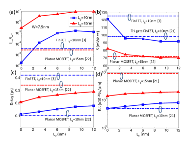
We plot the variation of the subthreshold slope as a function of in Fig. 2(b) which shows a significant improvement of subthreshold slope with an increase in . In particular, we are able to pull down the slope from mV/dec to mv/dec for a nm channel length device by altering the underlap length. Here again, the sensitivity of the subthreshold slope reduces significantly at relatively larger underlap. It is also noticed that with a suitable underlap, HFinFET can provide improved subthreshold slope as compared to published data on MOSFET and FinFET of comparable gate lengths.
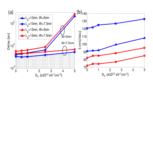
Fig. 2(c) and (d) reflect the degradation of intrinsic gate delay and the energy-delay product as a function of the underlap length. It is observed that an increase in underlap length from zero to nm can cause a degradation of and in the intrinsic delay, for =nm and nm respectively. Thus, it is important to carefully choose the underlap length to meet the delay requirements. We notice a similar degradation in the energy-delay product numbers as well with an increase in underlap length.
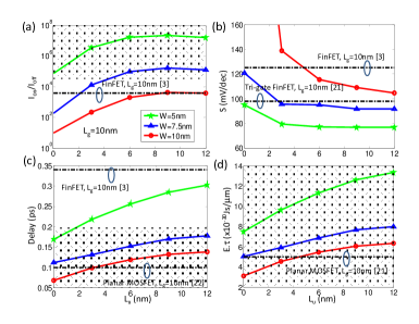
In Fig. 3, we plot the HFinFET characteristics as a function of with different fin widths for a fixed of nm. The shaded spaces indicate the regions which meet the specifications prescribed by ITRS 2009. As expected, with an increase in the fin width, the sensitivity of the characteristics due to a change in the underlap increases. We note that, in Fig. 3(a), even with a large underlap, the =nm case is not able to meet the ITRS projection for on-off ratio. However, with smaller width, it can be met at suitable underlap. The subthreshold slope in Fig. 3(b) has a strong degradation with increase in fin width due to stronger source-drain coupling, which can be effectively reduced by increasing the underlap. We clearly notice from Fig. 3(c) that even with sufficiently large underlap, we are able to meet the ITRS projection for delay with nm. However, for smaller fin width (=nm), it is difficult to meet the projection for any significant underlap. However, as we see from 3(d), the predicted energy-delay products are safely within the limit of ITRS projection for any width and underlap combination. This clearly indicates the small switching charge in the device operation due to strong energy quantization arising from both low carrier effective mass as well as geometric confinement of the carrier wave function. All these projected numbers compare very well against published planar and non-planar Si MOSFET data.
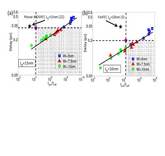
We show the transistor characteristics in the delay versus on-off ratio space for both =nm and nm in Fig. 4(a) and (b) respectively. In both the plots, for a given fin width, an increase in underlap shifts the operating point towards the top right corner. Interestingly, for =nm, there is no =5nm point that falls inside the shaded region that satisfies ITRS projection due to excessive intrinsic delay and this remains true for any underlap. On the other hand, for =nm, the operating points with =nm lie outside the projected region due to poor on-off ratio. Also, note that, at smaller fin width, there is comparatively larger spread of gate delay and less spread in on-off ratio for different underlap lengths. However, the converse is true for larger fin widths. As expected, a less number of points satisfy ITRS projection for =nm as compared to =nm.
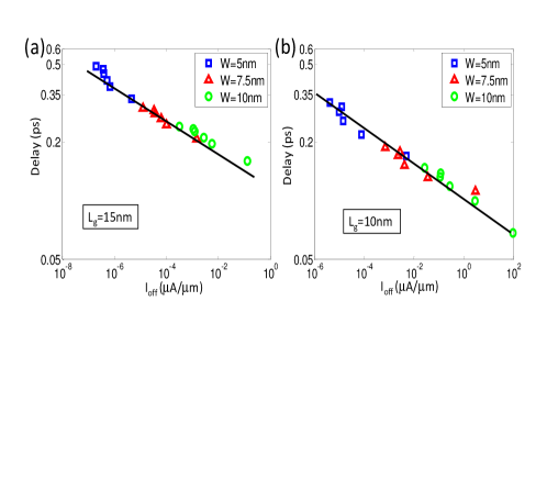
Finally, in Fig. 5(a) and (b), the intrinsic gate delay of the HFinFET is plotted as a function of off current, for different fin widths and underlap lengths. It is shown that for both the gate lengths, at a given fin width, an increased underlap significantly improves the off current, though at the cost of marginal delay degradation.
IV Effects of Interface Traps
In spite of intense research on improving the interface quality of gate dielectric and III-V channel material [12]-[14], to date, it remains one of the technological roadblocks that need to be overcome. In this section, we assume a uniform distribution of the interface trap density in the bandgap of the channel material at the channel-dielectric interface and examine its effects on the HFinFET characteristics.
Importantly, the presence of interface traps increases the parasitic capacitance which in turn reduces the fraction of useful (mobile) channel charge in the total charge that is switched during device operation [20]. This effect is more prominent as we reduce the fin width since this in turn reduces the quantum capacitance of the channel due to stronger energy quantization arising from geometrical confinement. This is explained in Fig. 6(a) where we plot the intrinsic gate delay as a function of the trap density for different channel lengths and fin widths with a zero underlap. It is observed that the gate delay is less dependent on for relatively wider fins, but for the narrower ones, the delay increases drastically. Larger drives the operating point away from the region allowed by the ITRS projection. In Fig. 6(b), it is observed that for a given channel length and fin width, the subthreshold slope degrades almost linearly with an increase in .
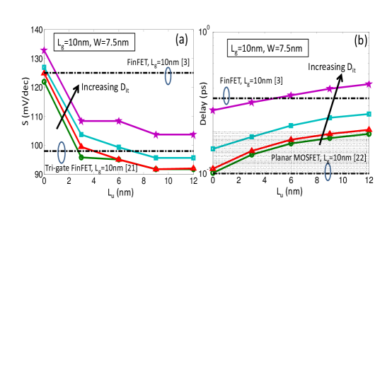
We now show that this increase in subthreshold slope due to increased can again be brought back to lower numbers by an increase in underlap, as explained in Fig. 7(a). At sufficiently larger underlap, the predicted subthreshold slope values outperform the Silicon non-planar data [3, 21], even at significantly large trap density. The degradation in delay due to the increased underlap is shown in Fig. 7(b) and can be comfortably controlled to keep within ITRS limit, unless the interface is extremely poor.
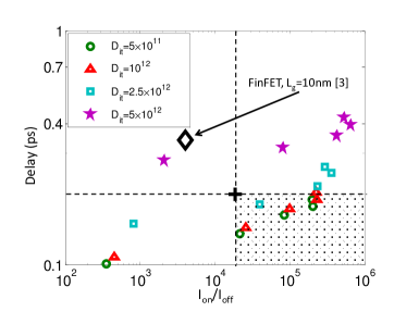
Finally, we have plotted the performance of HFinFET in presence of and in the delay versus on-off ratio space in Fig. 8. We notice that there is no point that meets the ITRS projections for =cm-2eV-1, even at large underlap lengths. However, at smaller trap density, there is an allowed window whose size strongly depends on the quality of the channel-dielectric interface. Nonetheless, the underlap parameter can be indirectly used to mitigate this technological challenge of obtaining improved channel-dielectric interface.
V Conclusion
To conclude, we have performed a 3-D simulation study to investigate the effects of introducing a varying gate-source and gate-drain underlap to show that it provides a unique way to meet either high performance or low power requirements for the HFinFET. It has been shown that the effect of the underlap strongly depends on the fin width as well as the channel length of the transistor. The performance degradation of HFinFET has been studied in presence of traps at the channel-dielectric interface. Finally, it has been shown that an underlap can be used to recover the degraded subthreshold slope and on-off ratio, meeting the intrinsic gate delay projection by ITRS 2009.
References
- [1] [Online]. Available: http://www.itrs.net/Links/2009ITRS/2009Chapters 2009Tables/2009PIDS.pdf
- [2] Y. K. Choi, N. Lindert, P. Xuan, S. Tang, D. Ha, T. Anderson, S. J. King, J. Bokor and C. Hu, “Sub-20nm CMOS FinFET Technologies,” IEDM Tech. Dig., pp. 412-424, 2001.
- [3] B. Yu et al., “FinFET Scaling to 10nm Gate Length,” IEDM Tech. Dig., pp. 251-254, 2002.
- [4] F. L. Yang et al., “5nm-Gate Nanowire FinFET,” Symp. VLSI Tech., pp. 196-197, 2004.
- [5] D. H. Kim and J. A. Del Alamo, “Logic Performance of 40nm InAs HEMTs,” IEDM Tech. Dig., pp. 629-633, 2007.
- [6] D. H. Kim and J. A. Del Alamo, “30nm E-mode InAs PHEMTs for THz and Future Logic Applications,” IEDM Tech. Dig., pp.719-722, 2008.
- [7] S. Datta et al., “85nm Gate Length Enhancement and Depletion mode InSb Quantum Well Transistors for Ultra High Speed and Very Low Power Digital Logic Applications,” IEDM Tech. Dig., pp. 763-766, 2005.
- [8] K. Majumdar, P. Majhi, N. Bhat and R. Jammy, “HFinFET: A Scalable, High Performance, Low Leakage Hybrid n-Channel FET,” IEEE Trans. Nanotech, Vol. 9, No. 3, pp. 342-344, 2010.
- [9] J. G. Fossum, M. M. Chowdhury, V. P. Trivedi, T.-J. King, Y.-K. Choi, J. An, and B. Yu, “Physical Insights on Design and Modeling of Nanoscale FinFETs,” in IEDM Tech. Dig., 2003, pp. 679-682.
- [10] V. Trivedi, J. G. Fossum, M. M. Chowdhury, “Nanoscale FinFETs With Gate-Source/Drain Underlap,” IEEE Trans. Elec. Dev. Vol. 52, No. 1, pp. 56-62, 2005
- [11] K. D. Cantley Y. Liu, H. S. Pal, T. Low, S. S. Ahmed and M. S. Lundstrom, “Performance Analysis of Ill-V Materials in a Double-Gate nano-MOSFET,” in IEDM Tech. Dig., 2007, pp. 113-116.
- [12] N. Goel, D. Heh, S. Koveshnikov, I. Ok, S. Oktyabrsky, V. Tokranov, R. Kambhampati, M. Yakimov, Y. Sun, P. Pianetta, C. K. Gaspe, M. B. Santos, J. Lee, S. Datta, P. Majhi, andW. Tsai, Addressing the gate stack challenge for high mobility InxGa1-xAs channels for NFETs, in IEDM Tech. Dig., 2008, pp. 363-366.
- [13] J. Huang, N. Goel, H. Zhao, C. Y. Kang, K. S. Min, G. Bersuker, S. Oktyabrsky, C. K. Gaspe, M. B. Santos, P. Majhi, P. D. Kirsch, H. H. Tseng, J. C. Lee, and R. Jammy, “InGaAs MOSFET performance and reliability improvement by simultaneous reduction of oxide and interface charge in ALD (La)AlOx/ZrO2 gate stack,” in IEDM Tech. Dig., 2009.
- [14] Z. Han and J. C. Lee, “Self-aligned In0.53Ga0.47As MOSFETs with atomic layer deposited Al2O3, ZrO2, and stacked Al2O3/ZrO2 gate dielectrics,” in IEEE Int. Conf. IC Des. Tech, 2009, pp. 229-232.
- [15] M. Passlack, K. Rajagopalan, J. Abrokwah, and R. Droopad, “Implant-Free High-Mobility Flatband MOSFET: Principles of Operation,” IEEE Trans. Elec. Dev., Vol. 53, No. 10, pp. 2454-2459, 2006.
- [16] K. Natori, “Ballistic metal-oxide-semiconductor field effect transistor,” J. Appl. Phys., Vol. 76, No. 8, pp. 4897, 1994.
- [17] A. Rahaman, J. Guo, S. Datta and M. Lundstrom, “Theory of Ballistic Nanotransistors,” IEEE Trans. Elec. Dev., Vol. 50, No. 9, pp. 1853 - 1864, 2003.
- [18] K. Majumdar and N. Bhat, “Bandstructure effects in ultra-thin-body double-gate field effect transistor: A fullband analysis,” J. Appl. Phys., Vol. 103, pp. 114503, 2008.
- [19] H. S. Pal T. Low and M. S. Lundstrom, “NEGF Analysis of InGaAs Schottky Barrier Double Gate MOSFETs,” IEDM Tech. Dig., 2008.
- [20] K. Majumdar, N. Bhat, P. Majhi and R. Jammy, “Effects of Parasitics and Interface Traps on Ballistic Nanowire FET in the Ultimate Quantum Capacitance Limit,” IEEE Trans. Elec. Dev., Vol. 57, No. 9, pp. 2264-2273, 2010.
- [21] R. Chau, S. Datta, M. Doczy, B. Doyle, B. Jin, J. Kavalieros, A. Majumdar, M. Metz, and M. Radosavljevic, “Benchmarking Nanotechnology for High-Performance and Low-Power Logic Transistor Applications,” IEEE Trans. Nanotech., Vol. 4, No. 2, pp. 153-158, 2005.
- [22] R. Chau, B. Doyle, M. Doczy, S. Datta, S. Hareland, B. Jin, J. Kavalieros, and M. Metz, “Silicon Nano-Transistors and Breaking the 10nm Physical Gate Length Barrier,” Dev. Res. Conf., pp. 123-126, 2003.