Development of the analog ASIC for multi-channel readout X-ray CCD camera
Abstract
We report on the performance of an analog application-specific integrated circuit (ASIC) developed aiming for the front-end electronics of the X-ray CCD camera system onboard the next X-ray astronomical satellite, ASTRO-H. It has four identical channels that simultaneously process the CCD signals. Distinctive capability of analog-to-digital conversion enables us to construct a CCD camera body that outputs only digital signals. As the result of the front-end electronics test, it works properly with low input noise of 30V at the pixel rate below 100 kHz. The power consumption is sufficiently low of 150 mW/chip. The input signal range of 20 mV covers the effective energy range of the typical X-ray photon counting CCD (up to 20 keV). The integrated non-linearity is 0.2 % that is similar as those of the conventional CCDs in orbit. We also performed a radiation tolerance test against the total ionizing dose (TID) effect and the single event effect. The irradiation test using 60Co and proton beam showed that the ASIC has the sufficient tolerance against TID up to 200 krad, which absolutely exceeds the expected amount of dose during the period of operating in a low-inclination low-earth orbit. The irradiation of Fe ions with the fluence of 5.2108 Ion/cm2 resulted in no single event latchup (SEL), although there were some possible single event upsets. The threshold against SEL is higher than 1.68 MeV cm2/mg, which is sufficiently high enough that the SEL event should not be one of major causes of instrument downtime in orbit.
keywords:
X-ray , ASIC , CCD camera1 Introduction
X-ray CCD (charge-coupled device) camera has achieved primary roles in X-ray astronomy thanks to its well-balanced performances: a moderate energy resolution of 130 eV (FWHM) @ 5.9 keV [1, 2, 3], a satisfactorily high quantum efficiency in the wide energy range from 0.3 to 12 keV, and a high positional resolution of 10 m. Conventional frame-transfer CCDs equip one readout node per several millions of pixels. To process the frame image in several seconds, the readout electronics tend to be very large and power-dissipated.
Recently some payloads in astronomical satellites adopt application-specific integrated circuit (ASIC) to achieve extremely lower power consumption and smaller size of the electronics than those made of discrete ICs [4, 5, 6]. Meidinger et al. [7] reported that their CCD camera system for a future astronomical mission with a thick (450 m), fully depleted pnCCD and ASIC chip proved the low readout noise of 2 e- rms and fast pixel rate of 13 MHz. All of the above ASICs, however, only manipulate analog signals or barely have a discriminator. To suppress the potential readout noise more strictly, therefore, we have been developing an analog complementary Metal-Oxide-Semiconductor (CMOS) ASIC with an analog-to-digital (AD) conversion capability and placed it next to the CCD. We employed modulators [8] as the AD converter (ADC) since this type of ADC can achieve a high resolution at a moderately short conversion time and functions not only as an ADC but also a band-pass filter.
The main objective of our ASIC is the ASTRO-H satellite [9], Japanese X-ray astronomical satellite that will be launched in 2014. The X-ray CCD camera (SXI: Soft X-ray Imager) [10] takes a role of the primary X-ray imager. It consists of four CCD chips that are abutted into a 2 by 2 array. Each chip has an imaging area of 1280 1280 pixels and four readout nodes. Given the focal length of 5.6 m, the four chips cover a region of 38 38 on the sky combined with the Soft X-ray Telescope [11]. SXI will utilize back-illuminated (BI) chips, with a thick depletion layer of 200 m. Then effective energy range will be 0.4 - 12 keV, which bridges the ranges of other instruments, the Soft X-ray Spectrometer (0.3 - 10 keV) [12] and the Hard X-ray Imager (5 - 80 keV) [13].
As well as the basic functions and performances as the front-end electronics of SXI, the radiation tolerance must be investigated to verify the functionality on the planned orbit throughout the mission lifetime. The radiation damage to the MOS Field-Effect Transistors (MOSFETs) causes a total ionizing dose (TID) effect and a single event effect (SEE). As a result of the TID effect, which is due to the protons and electrons, the leak current increases, the threshold voltages of MOSFETs change, and the 1/ noise increases [14]. The SEE, caused by heavy-ions in cosmic-rays, produces many hole-electron pairs in a specific MOSFET, hence causes non-destructive SEE such as single event upset (SEU) or destructive SEE such as single event latchup (SEL). Gamma-rays and particle beams are usually used to evaluate the threshold level against the TID effect and the SEE.
2 Description of the ASIC
 |
Basic circuit configuration of our ASIC (hereafter we call it MND02) is the same as that of MD01[15]. Here we summarize its specification that characterizes our CCD camera system.
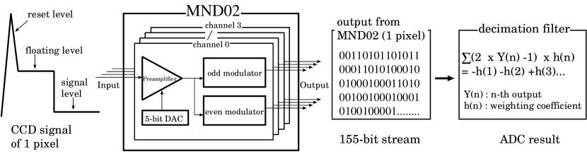
It was implemented through Taiwan Semiconductor Manufacturing Company (TSMC) 0.35 m CMOS process and then the 3 mm square bare chip is packed into 15 mm square ceramic quad flat pack. The signal process in MND02 is shown in figure 1. It works with 3.3 V power supply for analog and digital circuits. Four identical circuits (from channel 0 to 3) process the CCD signals simultaneously. Each circuit consists of a preamplifier, a 5-bit digital-to-analog converter (DAC), and two modulators. Input signals are at first amplified with adjustable gain from 0.6 to 10 in 9 steps. The signal from CCD consists of reset, floating and signal levels. The voltage difference between the latter two levels depends on the amount of electrons transferred by CCD. However, there is a difference between these levels even in the case of no signal charge due to the readout clocking pulse, which results as an offset in the ‘energypulse height’ relation. To minimize this offset and to effectively use MND02’s input signal range, we put an offset voltage to the signal level by 5-bit DAC. Then modulators [16] take oversampling for these levels and integrate them.We measure the voltage difference by integrating two levels with opposite polarity. This multiple sampling by the modulators shifts the majority of the quantization noise above the signal band in the frequency spectrum. Finally it converts the analog signal of one pixel to a digital 155-bit stream. Two (“even” and “odd”) modulators work alternately to improve the readout speed.
The bit stream is decoded by the decimation filter that is implemented in the Field Programmable Gate Array to obtain a 12-bit decimal value. We have determined the weighting coefficients for each bit in the filter by simulations of our circuits (figure 6 in [15]) to upgrade the frequency response as a low-pass filter and improve the signal-to-noise ratio.
3 Performance as a Front-end Electronics
We describe the results of the front-end electronics tests of MND02. Pseudo CCD signals with constant input voltage were input for all of four channels simultaneously. We tested 18 voltage levels throughout the input signal range from –20 to +20 mV and obtained 819 pixel data from each voltage level. Gain of the preamplifier was always set to be 10. Readout rates were 1.25 MHz and its divisors of 2 until 19.5 kHz, which is determined by the quartz crystal unit on the test module.
The power consumption was measured by comparing the current in the printed circuit board (PCB) between the case when MND02 was mounted and that when it was not on the PCB (upper panel of figure 2). Although the current increases with the readout rate, the power consumption of the entire chip is about 150 mW at the pixel rate below 100 kHz. In the middle panel of figure 2, we show the noise performance of MND02. The statistical uncertainty of the decimal values was measured from 819 pixel data for each input voltage and we took the average of 18 data sets taken with different voltage levels. We confirmed that the average noise was suppressed to be less than 30 V at the pixel rate below 100 kHz. Integrated non-linearity (INL) was also measured from the linearity plot (figure 3) for each readout rate as shown in the bottom panel of figure 2. Moderate INL of approximately 0.2% was obtained below 100 kHz.
 |
 |
 |
 |
4 Radiation Tolerance
The first space application of MND02 will be the ASTRO-H satellite that will be put into a low-earth orbit (LEO) with a height of 550 km and an inclination angle of 30 . The primary causes of the integrating damage in the LEO are protons and electrons that penetrate a package when the satellite passes through the South Atlantic Anomaly. We calculated the expected dose rate of Silicon assuming the thickness of the Aluminum cover of 1 mm using the dose model of SHIELDOSE-2111http://see.msfc.nasa.gov/ire/models.htm. AP8 and AE8 models are employed for the proton and electron spectra, respectively. The dose rate obtained is 1.1 krad/year in this orbit. Considering that the typical mission lifetime is 10 years and that we should count the twice of margin, we require a tolerance of 22 krad against the TID effect.
4.1 Gamma-ray Test
We adopted the 60Co (1.1 and 1.3 MeV) gamma-ray irradiation facility at Radiation Research Center, Osaka Prefecture University on 1 - 2 June 2009 for the TID effect test. No CCD was connected to the PCB and alternatively pseudo CCD signals were input at a pixel rate of 78 kHz in the same manner as in the front-end electronics test. The cylindrical 60Co with a height of 30 cm, 10 mm, an intensity of 186 TBq, was pulled up from underground to start the irradiation. The ICs on the PCB except MND02 were protected by the lead with a thickness of 10 cm to suppress the gamma-ray intensity to be 10-3 of that for MND02. The distance from the source to MND02 was determined such that the intensity at the device under test was 28.6 krad/hour (200 krad in 7 hours). We performed the above signal processing for only one chip during the irradiation, while other five chips were biased, clocked but not processed. All of the test was performed in the room temperature (20 C), which is the expected nominal thermal environment for MND02.
|
|
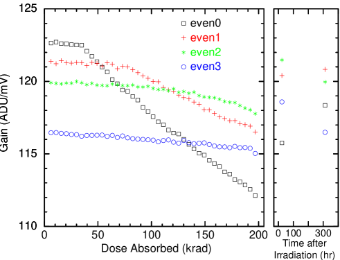
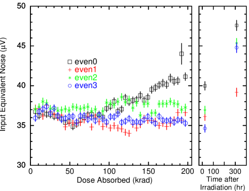
The current in MND02 increased by 10% during the test with a total dose of 200 krad. Figure 4 shows the gain variability as a function of the dose absorbed. One of the modulator, even0 exhibits the earliest and most remarkable gain degradation above 30 krad. Since a common behavior was seen between even and odd modulators in the specific channel and the degradation was gradual as a function of the dose absorbed, we think that the TID effect occurred in the preamplifier rather than the modulator. All the other five chips exhibited the same amount of degradation, and channel 0 in each chip showed the most remarkable degradation. Since four channels are identical in electric circuit point of view, the result suggests that there is an intrinsic weak point in the layout design of the bare chip. Nevertheless, the degree of the degradation is less than 10% even above 200 krad that corresponds to about 200 years in the LEO. Hence it will not cause the practical problem in orbit. Figure 5 also guarantees the stable noise performance of all the modulators during the mission lifetime expected.
The above performances were monitored also after the irradiating test to investigate the degree of the annealing effect in the room temperature. The right panels in figure 4 and 5 show the performance variability as a function of the time after the irradiation. The gain recovered in the post-irradiation test performed about two weeks after although the channel 0 seemed to be still in recovery progress. The transition of the input equivalent noise is a puzzle; all the six chips showed strong degradation after 300 hours. However, we performed the front-end electronics test again for the six chips about 16 months after the irradiation and found that the input equivalent noise recovered to the same level as those of non-irradiated chips. Hence we can say there is no permanent TID effect.
4.2 Proton/Fe ion test
To deal with the proton/Fe ion beam test, we utilized the synchrotron ring at Heavy Ion Medical Accelerator in Chiba (HIMAC) in National Institute of Radiological Sciences (NIRS) on 6 - 8 July 2009. A 150 MeV proton and a 400 MeV/amu Fe ion beam with a size of 2 mm FWHM were irradiated to MND02. These energy values were chosen since the irradiation facility for physics in HIMAC has many achievements for the value. Since the bare chip is 3 mm square, the efficiency that the particle hit the chip was calculated considering the two-dimensional profile of the beam. All of the dose and fluence value hereafter are calculated considering the efficiency. Table 1 summarizes the specification of both beams.
| Species | Proton | Fe ion |
|---|---|---|
| Energy (MeV/amu) | 150 | 400 |
| Max. intensity (Ion/sec/cm2) | 6.2108 | 1.3106 |
| Linear energy transfer | 4.3810-3 | 1.68 |
| (MeV cm2/mg) |
We were anxious about possible performance change of the ASIC just after being put into the orbit. Hence we began the test with relatively low intensity of 2.9 krad/hour until the total dose amounted to be 0.7 krad. Since we confirmed that there was no performance change, we increased the beam intensity to 158 krad/hour to measure the TID tolerance. The total dose absorbed was 167 krad through our experiment. Both of the two chips under the test showed no performance degradation nor increase of the current including the post-irradiation test. This is inconsistent with the result we observed in the 60Co test. We suspect that the estimation of the dose rate with 60Co is relatively ambiguous compared with that with protons. We calibrated the dose rate in the 60Co irradiation facility using an ionization chamber and we needed to convert the exposure dose to the absorbed dose for silicon. There may be some uncertainty in these calibration processes.
These results exhibit the significant improvement of the TID tolerance compared with that of the previous version of the ASIC, MD01 [17]. The fabrication process of MD01 is the same as that of MND02, although the former chip was packaged in the plastic QFP. There is also no change for the experiment condition from the previous one except that the energy of the proton was 200 MeV and that the intensity was slightly higher than that of this work. This leads us to attribute the lack of the TID tolerance of MD01 to the circuit design and/or the layout design. The major difference in the circuit design between MND02 and MD01 is in the preamplifier; MND02 equips P channel MOSFETs at the first amplifying stage since the P channel MOSFETs generally exhibit lower 1/ noise than that of the N channel MOSFETs. The size of the first stage FET in MND02 was set to be larger than that in MD01. Although these revisions were designed for lower noise performance, we found the radiation tolerance improved.
We tested three chips for Fe ion beam. The total fluence of the former two chips were 1.5107 Ion/cm2 while that for the last chip was 5.2108 Ion/cm2. We performed functional test in the same manner as in the 60 Co test and monitored the current in the PCB for analog and digital circuits. These values were 14 - 15 mA and 119 - 120 mA for analog and digital circuits throughout the irradiation, respectively. We found no peculiar increase of the current, that is, no SEL occurred in the test. Hence the cross section against the SEL () was estimated assuming an upper limit of three events for the fluence to be cm2/(IonASIC) at the LET of 1.68 MeV cm2/mg at 95% confidence level. This LET is sufficiently high enough that SEL event should not be one of major causes of instrument downtime even if the recovery requires power cycle of the instrument.


Figure 6 shows the distribution of the decimal pulse height for the data of 819 pixels with a constant input voltage. We observed some anomalous pixels with the deviation of about 20 - 80 ADU from the distribution center during the irradiation. We calculated using the weighting coefficients of the decimation filter that the typical magnitudes of the deviation should be about 120 ADU if we assume a single-bit upset in the 155-bit stream. Hence the result suggests that the upset occurred not in the output flip-flops. Then the suspected origin is that some charges are injected into the integrators in the modulators or some capacitors in the preamplifiers. The cross section of the SEU at the LET of 1.68 MeV cm2/mg was calculated to be cm2/(Ionbit).
Future work to board our ASIC on ASTRO-H is to obtain the LET threshold of and in order to estimate the SEE rate in the LEO. The burn-in test and the thermal functional test will also be performed.
5 Summary
We summarize the results of the front-end electronics test and the radiation tolerance test of MND02 as follows:
-
1.
As a result of the front-end electronics test, it works properly with low input noise of 30V at the pixel rate below 100 kHz. The power consumption is sufficiently low of 150 mW/chip. The INL is 0.2 % throughout the input signal range from –20 to +20 mV, which is similar performance to the conventional electronics in orbit.
-
2.
The radiation tolerance against the TID effect was estimated by using 60Co and the 150 MeV proton beam. The gain and input equivalent noise were stable until the dose of 30 krad absorbed for the former test. Considering the expected dose rate of 1.1 krad/yr in the LEO of ASTRO-H, the radiation tolerance of MND02 indicates the proper operation for more than 20 years.
-
3.
Fe ion beam test with the LET of 1.68 MeV cm2/mg and the fluence up to 5.2108 Ion/cm2 showed no SEL. The threshold against the SEL is higher than 1.68 MeV cm2/mg, which is sufficiently high enough that the SEL events should not be one of major causes of the instrument downtime.
We acknowledge Assistant Professor Takao Kojima of Osaka Prefecture University and Hidenobu Mori who offered us much support and encouragement in the 60Co experiment. This work is partly supported by the Nano-Satellite Research and Development Project in Japan and the Research Project with Heavy Ions at NIRS-HIMAC.
References
- [1] A. D. Short, A. Keay, M. J. Turner, Proc. SPIE 3445 (1998) 13 27
- [2] G. P. Garmire, M. W. Bautz, P. G. Ford, J. A. Nousek, G. R. Ricker, Jr., Proc. SPIE 4851 (2003) 28 44
- [3] K. Koyama et al., PASJ 59 (2007) S23 S33
- [4] R. Rando, A. Bangert, D. Bisello, A. Candelori, P.Giubilato, M. Hirayama, R. Johnson, H. F.-W. Sadrozinski, M. Sugizaki, J. Wyss, M. Ziegler, IEEE Trans. Nucl. Sci. 51 (2004) 1067 1073
- [5] H. Tajima, T. Nakamoto, T. Tanaka, S. Uno, T. Mitani, Ed. Ce. Silva, Y. Fukazawa, T. Kamae, G. Madejski, D. Marlow, K. Nakazawa, M. Nomachi, Y. Okada, T. Takahashi, IEEE Trans. Nucl. Sci. 51 (2004) 842 847
- [6] S. Herrmann, W. Buttler, R. Hartmann, P. Holl, N. Meidinger, L. Strüder, Nuclear Science Symposium Conference Record, IEEE 3 (2007) 2398 2403
- [7] N. Meidinger R. Andritschke, O. Hälker, R. Hartmann, S. Herrmann, P. Holl, G. Lutz, N. Kimmel, G. Schaller, M. Schnecke, F. Schopper, H. Soltau, L. Strüder, Nucl. Instr. and Meth. A 568 (2006) 141 148
- [8] H. Inose, Y. Yasuda, J. Murakami, IRE Trans. on Space Electronics Telemetry SET-8 (1962) 204-209
- [9] T. Takahashi et al., Proc. SPIE 7732 (2010) 77320Z
- [10] H. Tsunemi et al., Proc. SPIE 7732 (2010) 773210
- [11] H. Awaki et al., Proc. SPIE 7437 (2009) 743703
- [12] K. Mitsuda et al., Proc. SPIE 7732 (2010) 773211
- [13] M. Kokubun et al., Proc. SPIE 7732 (2010) 773215
- [14] D. M. Fleetwood, H. D. Xiong, R. D. Schrimpf, Z. -Y. Lu, C. J. Nicklaw, J. A. Felix, R. D. Schrimpf, S. T. Pantelides, IEEE Trans. Nucl. Sci. 49 (2002) 2674 2683
- [15] D. Matsuura, H. Nakajima, E. Miyata, H. Tsunemi, J. P. Doty, H. Ikeda, Proc. SPIE 6686 (2007) 66860L
- [16] J. P. Doty, D. Matsuura, H. Ozawa, E. Miyata, H. Tsunemi, H. Ikeda, Proc. SPIE 6276 (2006) 62761P
- [17] H. Nakajima, D. Matsuura, N. Anabuki, E. Miyata, H. Tsunemi, J. P. Doty, H. Ikeda, T. Takashima, H. Katayama, IEEE Trans. Nucl. Sci. 56 (2009) 747 751