Anomalous Enhancement of the Superconducting Transition Temperature in Electron-Doped Cuprate Heterostructures
Abstract
The superconducting transition temperature of multilayers of electron-doped cuprates, composed of underdoped (or undoped) and overdoped La2-xCexCuO4 (LCCO) and Pr2-xCexCuO4 (PCCO) thin films, is found to increase significantly with respect to the of the corresponding single-phase films. By investigating the critical current density of superlattices with different doping levels and layer thicknesses, we find that the enhancement is caused by a redistribution of charge over an anomalously large distance.
pacs:
74.78.Fk, 74.72.Ek, 74.72.-h, 74.25.SvOne of the striking properties of the high– cuprates is the strong dependence on the number of charge carriers put into the CuO2 planes of many of their electronic properties. For example, for low carrier concentration (underdoped regime) the material is insulating; it is metallic for high carrier concentration (overdoped regime), and superconducting in between, with a maximal for the optimum doping. The charge carriers can be either holes or electrons.GreeneRMP
Recently, it has been shown that heterostructure bi-layers (BL’s) and super-lattices (SL’s), composed of metallic and insulating hole-doped cuprates, can be superconducting.Bozovic2008 ; Smadici2009 Also, a BL of superconducting La2-xSrxCuO4 (LSCO) and metallic, nonsuperconducting La1.65Sr0.35CuO4 has a critical temperature () greater than the superconducting single-phase LSCO itself, with a maximal enhancement for .Yuli2008 ; Millo2010 In this case, the superconducting layer was shown to be confined to the interface. The enhancement in Refs.4 and 5 has been interpreted in terms of an interplay between the large pairing amplitude in the underdoped (UD) cuprate and the phase stiffness originating from the metallic overdoped (OD) layer.Kivelson2008 In this model, in UD cuprates is not the temperature where the pairs are formed and condensed as in the BCS theory, but a temperature at which phase order is destroyed by fluctuations despite the persistence of pairing amplitude.Kivelson1995 Other possible explanations for the enhancement are: oxygen diffusion or uptake, strain induced by the substrate Locquet1998 and cationic diffusion between the layers. The latter was shown to be negligible for LSCO.Bozovic2008
In hole-doped cuprates, a large phase fluctuation region above has been observed by different techniques such as the Nernst effect and torque magnetization,Wang2006 ; Li2010 and scanning tunneling microscopy measurements.Gomes2007 ; Yuli2009 In contrast, in the electron doped cuprates, the pairing amplitude seems to follow even for the UD side,Dagan2009 and phase fluctuations appear to be small as indicated by the narrow region of vortex Nernst effect observed above .Li2007 The normal state tunneling gap was interpreted as preformed superconductivity, however, this gap vanished at rather low temperature, not very far away from for UD samples.Dagan2005 If the interplay between the pairing amplitude in the UD layer and the phase stiffness in the OD layer is the origin of the enhancement in cuprate SL’s one would expect a smaller enhancement for electron-doped heterostructures.
Here we report a large enhancement in electron-doped cuprate heterostructures of both La2-xCexCuO4 (LCCO) and Pr2-xCexCuO4 (PCCO) SL’s. This large enhancement argues against an increased phase stiffness in the UD layer as proposed in Ref.6. However, we find that the critical current of the SL’s scales with the total layer thickness and not with the number of interfaces. This suggests that the observed enhancement is not confined to the interfaces but is caused by a global redistribution of charge carriers. In addition, we find that the of the SL’s scales with the -axis lattice parameter as found in single-phase PCCO films.Maiser1998 From these results we conclude that the enhancement in electron-doped SL’s is caused by an anomalous charge redistribution over a very large length scale of at least 20 nm. Our results suggest that the enhancement found in hole-doped cuprates may have the same origin.

Epitaxial films were grown on SrTiO3 (STO) substrates by the pulsed laser deposition (PLD) method.jk2009 ; Dagan2004 We took extra care optimizing the annealing conditions for each geometry and composition to obtain the maximal . LCCO is chemically stable for 0.06 whereas it has a contaminative T-phase for lower Ce concentrations.Naito2002 ; Sawa2002 PCCO can be deposited with . SL’s of LCCO were prepared with successive layers of (UD) and OD layer with and 0.21. For PCCO SL’s we used consecutive layers of (OD) and PCCO with and 0.12. BL’s of PCCO are composed of and . For all the SL’s in this study the total thickness is kept nm, and each layer has the same thickness. We use the notation (/0.06)n for interfaces between alternate OD LCCO ( and 0.21 and UD , as seen in the inset of Fig. 3(c) for (0.19/0.06)n.
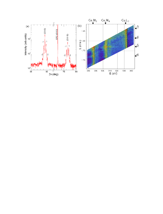
Figure 1(a) presents x-ray diffraction (XRD) spectra of LCCO sample (0.19/0.06)n=10, which has 11 layers with each layer nm ( 10 u.c.). Well-defined multiple satellite peaks originated from the modulated structure can be observed along with the main peaks of single-phase films. This confirms the periodic layered structure. The modulation period can be calculated from , where and represent two nearest satellite peaks.Zhu2007 From our data we obtain nm, consistent with the expected 20 u.c. periodicity from the deposition rate. Resonant soft x-ray scattering Smadici2009 for (0.19/0.06)n=10 sample show a SL modulation at the Ce edges. As seen in Fig. 1(b), several satellite peaks that coincide with the positions predicted from the above equation with are clearly visible at 910 eV (Ce M4 edge) and 890 eV (Ce M5 edge), respectively. This observation indicates that the SL reflections really arise from a selective modulation in the Ce density, whereas the Cu atoms reside in their usual, lattice positions. We also did an electron energy-loss spectroscopy (EELS) measurement on a similar SL film and found a clear Ce modulation.
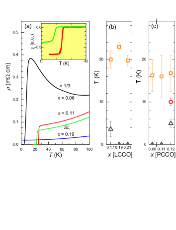
Figure 2(a) shows one example of enhancement in a LCCO SL, (0.19/0.06)n=10. The single-phase films have a broad transition with onset transition temperature K; the OD is metallic and nonsuperconducting. After constructing the SL, the of (0.19/0.06)n=10 reaches up to 24 K, comparable to the value of optimal doping with K. The real part of the ac susceptibility for (0.19/0.06)n=10 and single-phase are shown in the inset of Fig. 2(a). In Fig. 2(b) and (c), the transition temperatures (zero resistance of superconducting transition) and are plotted against the doping for LCCO and PCCO, respectively. All the SL’s show an obvious enhancement with respect to the single-phase films themselvesalmost constant for either LCCO with varying OD layer or PCCO with varying UD layerand are higher than that of BL’s. Since for the SL the enhancement is not small, the question naturally arises as to what mechanism is responsible for this enhancement.
One possible explanation is a substrate strain effect, which is expected to be important in very thin films.Locquet1998 ; Bozovic2002 In our experiment the thickness of the bottom layer changed from 5 nm to 20 nm while remained approximately constant. It is therefore unlikely that the enhancement is caused by strain.
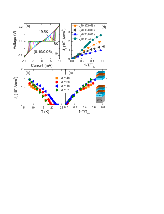
Next, we check if the enhancement in the SL is confined to the interface. Assuming well defined superconducting interfaces and a non-superconducting bulk film, the super-current should flow along the interfaces and “short-circuit” the entire film. In this scenario, one expects the critical current (I to scale with , the number of the interfaces.Ref In Fig. 3(a), typical current (I) - voltage (V) characteristics are shown for LCCO (0.19/0.06)n=40 at various temperatures. J is calculated from I) with the width of the current bridge and the total thickness of the film. Since both the and are kept the same for different SL’s, then J should be proportional to in the interface-effect scenario. We repeat these measurements for various ’s. In particular we measured LCCO (0.19/0.06)n with . These SL’s have approximately the same . Surprisingly, at all temperatures Jc is approximately independent of as seen in Fig. 3(b). In Fig. 3(c) we plot Jc for various ’s against the reduced temperature (). It can be clearly seen that Jc is not proportional to but approximately the same, so the enhancement is not confined to the interface! This can also rule out that the enhancement is caused by slight Ce diffusion, i.e., several unit cells at the interface. Note that our x-ray data [Fig. 1(b)] and EELS data (not shown) have excluded the case of heavy Ce diffusion since Ce modulation is clearly observed.

It has been reported that in La2CuO4 (LCO)/LSCO SL the conducting holes do not follow the distribution of the Sr atoms, and the LCO layers become highly doped. This suggests a redistribution of the charge carriers among the layers.Smadici2009 A similar effect must take place in our films, where, the charge carriers redistribute between the OD and UD layers. In the charge-redistribution scenario, the total effective thickness of the -enhanced region is determined by the Ce difference in the adjacent layers, irrespective of . Exactly how the charge redistributes is not known but our data in Fig. 3(c) suggest that this charge is spread over at least 20 nm since the Jc of (0.19/0.06)n is approximately the same for all ’s ( for , the layer thickness is nm). Fig. 3(d) shows the Jc data for SL’s with and 0.21, and also the single-phase film. We note that as increases the Jc of decreases. This is understandable in the charge-redistribution scenario since the -enhanced region with optimal charge count should be smaller as the Ce range becomes larger for the same total film thickness. Future and Jc experiments will be needed on thicker layers to determine a more definitive number for the anomalous length scale. We have attempted to make superlattices with and , but so far without success.

Fig. 4 presents versus c axis lattice parameter for LCCO films deposited in various techniques and SL’s with different annealing time. decreases on the overdoped side as decreases, both for SL’s and single phase films. Similar results were shown for single phase PCCO films with various Ce concentrations.Maiser1998 Since Ce4+ ion is smaller than Pr3+, this can explain the decrease of with increasing Ce doping as observed by Maiser et al..Maiser1998 In our case we observe a systematic change of with . This can be explained by charge redistribution in the SL’s causing an effect similar to that of Ce substitution in the single phase films. Since XRD is a bulk measurement the systematic variation of gives further indication that the charge redistribution occurs in the entire film thickness.
Oxygen diffusion is one plausible explanation for this charge redistribution over a very large distance. Unfortunately, the oxygen content in a single phase thin film or in various parts of a SL or BL cannot be precisely measured. Oxygen diffusion from UD to OD layers would increase since this would add carriers (electrons) to the UD layer. Higgins et al.Higgins2006 demonstrated that such a process increased the carrier concentration in the UD layers and decreased it in the OD ones. In that case, the enhancement will take place only in the UD layers, because for the overdoped layers the effect of carrier reduction is overwhelmed by the disorder introduced by the apical oxygen (the site of the added oxygen) resulting in a total decrease of .Higgins2006 So, oxygen diffusion from UD to OD layers appears to be a plausible explanation for the global charge redistribution. However, the oxygen diffusion length is of the order of the film thickness for the annealing temperature and time used in our deposition. Thus, it is difficult to explain using an oxygen diffusion scenario the difference between the BL, where the enhancement is relatively small, and the SL enhancement. Therefore, it is possible that the charge redistribution may have a different origin.

We tried to estimate the charge redistribution length scale () in a SL using a naive calculation. If we allow charge to move from the OD layer to the UD one, the electrostatic energy increases. However, the free energy can still decrease due to the enhanced superconductivity. Minimizing the free energy yields a length scale of the order of 0.2 Å, using the thermodynamic critical field H T and the charge density electronsCu (or holesCu). This means that the electrostatic energy is too high to explain the large length scale over which the charge redistributes in our experiment.
Another possibility is that charge redistribution occurs on a length scale determined by the screening length (). Using the Thomas-Fermi approximation we obtains a length scale of Å, which is two orders of magnitude smaller than what we observe. Certainly, this approximation is oversimplified for the cuprates. Yet, in the hole-doped LCO/LSCO SL an analysis of RSXS data yielded a screening length of Å,Smadici2009 not very different from our electron-doped results. So both the naively calculated and length scales are small and cannot explain the anomalously large charge redistribution length that is inferred by our experiments.
In conclusion, we fabricated electron-doped superlattice and bilayer films comprised of underdoped (or undoped) /overdoped La2-xCexCuO4 (LCCO) and Pr2-xCexCuO4 (PCCO), and find an enhanced which is comparable to optimally doped single-phase films for both LCCO and PCCO. Our results suggest that a charge carrier redistribution occurs on an anomalously large length scale of 20 nm. This charge redistribution is the cause for the enhancement. The exact mechanism of the charge redistribution is not known, although oxygen diffusion is the most plausible explanation. Further theoretical and experimental studies will be needed to understand these remarkable results.
The work at UMD is supported by NSF Grant DMR-0653535 and AFOSR-MURI Grant FA9550-09-1-0603, the work at Tel-Aviv and UMD by BSF Grant 2006385. RSXS studies were supported by the U.S. Department of Energy Grant No. DE-FG02-06ER46285, with use of the NSLS supported under Contract No. DE-AC02-98CH10886.
References
- (1) N. P. Armitage, P. Fournier and R. L. Greene, Rev. Mod. Phys. 82, 2421 (2010).
- (2) A. Gozar, G. Logvenov, L. F. Kourkoutis, A. T. Bollinger, L. A. Giannuzzi, D. A. Muller, and I. Bozovic, Nature (London) 455, 782 (2008).
- (3) S. Smadici, J. C. T. Lee, S. Wang, P. Abbamonte, G. Logvenov, A. Gozar, C. D. Cavellin, and I. Bozovic, Phys. Rev. Lett. 102, 107004 (2009).
- (4) O. Yuli, I. Asulin, O. Millo, and D. Orgad, Phys. Rev. Lett. 101, 057005 (2008).
- (5) A later study from G.Koren and O. Millo, Phys. Rev. B 81, 134516 (2010) reported that the results in Ref. [4] were not reproduced, but a small enhancement could still be observed.
- (6) E. Berg, D. Orgad, and S. A. Kivelson, Phys. Rev. B 78, 094509 (2008); S. Okamoto and T. A. Maier, Phys. Rev. Lett. 101, 156401 (2008); L. Goren and E. Altman, Phys. Rev. B 79, 174509 (2009).
- (7) V. J. Emery and S. A. Kivelson, Nature (London) 374, 434 (1995).
- (8) J.P. Locquet, J. Perret, J. Fompeyrine, E. Mächler, J. W. Seo, and G. V. Tendeloo, Nature (London) 394, 453 (1998).
- (9) Y. Wang, L. Li, and N.P. Ong, Phys. Rev. B 73, 024510 (2006).
- (10) L. Li, Y. Wang, S. Komiya, S. Ono, Y. Ando, G. D. Gu, and N. P. Ong, Phys. Rev. B 81, 054510 (2010).
- (11) K. K. Gomes, A. N. Pasupathy, A. Pushp, S. Ono, Y. Ando, and A. Yazdani, Nature (London) 447, 569 (2007).
- (12) O. Yuli, I. Asulin, Y. Kalcheim, G. Koren, and O. Millo, Phys. Rev. Lett. 103, 197003 (2009).
- (13) I. Diamant, R. L. Greene, and Y. Dagan, Phys. Rev. B 80, 012508 (2009).
- (14) P. Li and R. L. Greene, Phys. Rev. B 76, 174512 (2007).
- (15) Y. Dagan, M. M. Qazilbash, and R. L. Greene, Phys. Rev. Lett. 94, 187003 (2005).
- (16) E. Maiser, P. Fournier, J.-L. Peng, F. M. Araujo-Moreira, T. Venkatesan, R. L. Greene, and G. Czjzek, Physica C 297, 15 (1998).
- (17) K. Jin, X. H. Zhang, P. Bach, and R. L. Greene, Phys. Rev. B 80, 012501 (2009).
- (18) Y. Dagan, M.M. Qazilbash, C. P. Hill, V. N. Kulkarni, and R. L. Greene, Phys. Rev. Lett. 92, 167001 (2004).
- (19) M. Naito, S. Karimoto, and A. Tsukada, Supercond. Sci. Technol. 15, 1663 (2002).
- (20) A. Sawa, M. Kawasaki, H. Takagi, and Y. Tokura, Phys. Rev. B 66, 014531 (2002).
- (21) S. J. Zhu, J. Yuan, B. Y. Zhu, F. C. Zhang, B. Xu, L. X. Cao, X. G. Qiu, B. R. Zhao, and P. X. Zhang, Appl. Phys. Lett. 90, 112502 (2007).
- (22) A later study from I. Bozovic et al., Phys. Rev. Lett. 89, 107001 (2002) showed that the substrate strain effect was not the primary cause of the doubled reported in Ref. [9] .
- (23) IJ. Here J is the critical current density of the -enhanced part, which has effective thickness In the interface-effect scenario, should be determined by the proximity effect between adjacent layers, which is constant if the constituents are fixed. Thus, I.
- (24) P.G. Radaelli, J. D. Jorgensen, A. J. Schultz, J. L. Peng, and R. L. Greene, Phys. Rev. B 49, 15332 (1994).
- (25) J. S. Higgins, Y. Dagan, M. C. Barr, B. D. Weaver, and R. L. Greene, Phys. Rev. B 73, 104510 (2006).
- (26) B.X. Wu, K. Jin, J. Yuan, H.B. Wang, T. Hatano, B.R. Zhao, and B.Y. Zhu, Physica C 469, 1945 (2009).