Self heating and nonlinear current-voltage characteristics in bilayer graphene
Abstract
We demonstrate by experiments and numerical simulations that the low-temperature current-voltage characteristics in diffusive bilayer graphene (BLG) exhibit a strong superlinearity at finite bias voltages. The superlinearity is weakly dependent on doping and on the length of the graphene sample. This effect can be understood as a result of Joule heating. It is stronger in BLG than in monolayer graphene (MLG), since the conductivity of BLG is more sensitive to temperature due to the higher density of electronic states at the Dirac point.
pacs:
73.63.-b, 73.23.-b, 73.50.Fq, 72.80.VpI Introduction
Two-dimensional graphene in its monolayer and bilayer forms can exhibit rather different electronic characteristics.castroneto09 ; dassarma10b In monolayer graphene (MLG) the valence and conductance bands touch each other at two inequivalent Dirac points in the Brillouin zone, around which the bands are linear. Thus the density of states (DOS) also vanishes linearly around these points, where the Fermi energy of charge-neutral graphene is located. In the most common (Bernal) stacking of bilayer graphene (BLG) the two layers are electronically coupled such that the two linear bands of the individual layers mix to form four bands, the lower of which are parabolic around the Dirac points. In this case the DOS around these points is approximately constant.
This difference gives rise to different charge screening and transport properties for the two types of graphene. In particular, the temperature dependences for the conductivity of diffusive MLG and BLG around the charge-neutrality point (CNP) differ.adam07b ; morozov08 ; adam08 ; xiao10 ; adam10 ; dassarma10 In both cases, thermal excitation of quasiparticles from the valence to the conduction band (i.e. thermal creation of electron-like and hole-like charge carriers) increases the conductivity with temperature, as is typical for semiconductors and insulators. However, due to differences in the DOS, in MLG the conductivity at CNP grows only quadratically with temperature, while in BLG it increases linearly.adam08
In this paper we show how this difference of MLG and BLG is reflected in the current-voltage () characteristics of diffusive graphene. For MLG it is known that the characteristics tend to be linear at low bias voltage and have a tendency to saturate at higher voltages due to scattering of electrons from optical phonons.meric08 ; barreiro09 Close to CNP the at small can become superlinear as a result of Zener-Klein tunneling between the valence and conduction bands, especially in low-mobility samples.vandecasteele10 By measuring the curves of both MLG and BLG on a SiO2 substrate in a two-terminal configuration, we show that in BLG the characteristics have a much stronger tendency for superlinearity at V, which we associate with an increase of the conductivity due to self heating (Joule heating). This effect is only weakly dependent on the level of doping and on the length of the sample. We confirm this interpretation with numerical simulations using a semiclassical model based on Boltzmann theory for a diffusive two-dimensional (2D) system in quasiequilibrium. The model takes into account electron scattering from charged impurities, the band-bending effects due to charge doping by the metallic source and drain electrodes,huard08 ; barraza10 ; khomyakov10 uniform impurity doping, as well as nonuniform doping by a gate electrode. For MLG the Joule-heating-related nonlinearity is found to be weak, which is consistent with previous experiments and calculations.meric08 ; barreiro09 ; vandecasteele10
The paper is organized as follows. In Sec. II we introduce the theoretical model, Sec. III describes the experimental results and compares them to theory, and in Sec. IV we end with some discussion of other mechanisms for current nonlinearities. Details of the model are given in the Appendixes. In App. A solution of the electrostatic part of the problem in terms of a Green function is detailed. Appendix B discusses the modeling of the impurity scattering and gives expressions for the charge density and the transport coefficients for MLG and BLG. Finally, in Sec. C we discuss analytic semiclassical results for the temperature dependence of the conductance of a - junction, which can form in the graphene close to the metallic electrodes.
II Theoretical model
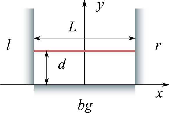
The model geometry that we consider (see Fig. 1) is a simplification of typical experimental geometries. It consists of a two-dimensional (quasi-one-dimensional) channel coupled to two transport electrodes ( and ) as well as a back gate electrode (). In this geometry we solve for the electrostatic potential together with transport equations for the quasiparticles in the channel.
Our semiclassical transport theory assumes a diffusive 2D electron system in quasiequilibrium,viljas10mod such that the quasiparticle distribution is described by a local chemical potential and a local temperature . A third unknown field is the electrostatic potential in the channel (), which shifts the energy of the local Dirac point such that . The three fields , , and are solved from the equations
| (1) |
Here prime denotes the -derivative, is the Green function of the Laplace operator, is the “characteristic function” for electrode (see App. A), and , where and are the relative and vacuum permittivities. Further, is the two-dimensional charge density in units of the electron charge (App. B), and is a phenomenological doping density that describes the doping effect by impurities, which is assumed to be constant. (Thus, charge puddlesmartin08 ; deshpande09 are not described — see below for discussion). The factors and are the charge and thermal conductivities, respectively, while and are the thermoelectric transport coefficients, satisfying . These factors are inversely proportional to the impurity density , which is taken to be another constant parameter independent of (App. B). The quantities , , , , and all depend on . Finally, is the Joule power per area, with being the electric current density, which is conserved, . The total current through a system of finite width is .
The boundary conditions at are chosen to be
| (2) |
which correspond to a voltage bias , assuming negligible contact resistance, the right-hand electrode to remain grounded, and both electrodes to remain at the bath temperature . The finite equilibrium chemical potential describes the effects of the work function mismatch and the resulting charge transfer between the graphene and the electrodes, with () leading to -type (-type) doping.khomyakov10
The first of Eq. (1) is the Poisson equation written as an integral equation at . The second and third describe current conservation and heat balance, respectively. Note that in order to keep the model simple, we do not include electron-phonon coupling and thus the Joule power is dissipated only via diffusion.viljas10mod This should be reasonable first approximation at bias voltages well below optical phonon energies.footnote2

In Fig. 2 we show typical results obtained from the model for BLG and MLG with parameters obtained from the fit to (the gate dependence of) our BLG experiments in Sec. III. It is to be noted that the aspect ratio is far too small for a simplified parallel-plate capacitor model to work properly in the geometry of Fig. 1, and a full numerical solution of Eqs. (1) is needed. The fields obtained as their solutions are very nonuniform, as shown for BLG in Fig. 3.
The upper panels of Fig. 2 are for the case of BLG. Fig. 2(a) shows the gate dependence of the linear-response conductivity , where is the resistivity. Due to finite positive doping density () the point of minimal conductivity (the apparent “CNP”) is shifted to V and as result of the lead-doping effect (), the gate dependence is asymmetrical around the CNP.huard08 Since the lead-doping is of type, at the BLG is of type everywhere. However, for two - junctions appear,huard08 and the BLG becomes of -- type. While for the dependence on temperature is relatively weak, for it is roughly linear: (Ref. adam08, ). For , where the - junctions dominate the resistance, it can be shown that approximately as (App. C). However, the theory is valid only when all parts of graphene remain far from the local CNP. This is because charge puddles, quantum-mechanical effects (see App. C), and a possible gap in the BLG spectrum are not taken into account. Thus, we mainly concentrate on the gate voltages .
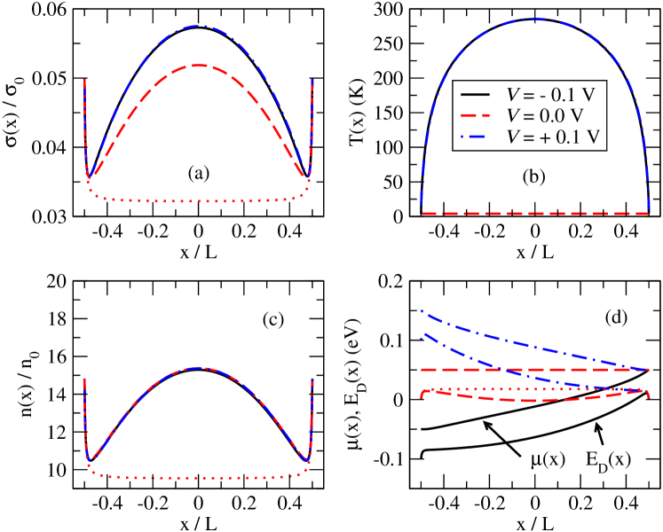
Fig. 2(b) shows the differential conductivity as a function of for a few gate voltages at low bath temperature. Note that the curves are nearly symmetric [], although there are small deviations, which are due to the asymmetrical choice of the boundary conditions and the presence of the gate electrode. The increase of at finite signifies a superlinear contribution to the curve: () with . This superlinearity is strongest close to the CNP, where the conductivity of BLG is most sensitive to temperature (see Eq. (9)). In fact, the increase of the conductivity with voltage [see Fig. 3(a)] is entirely due to heating, which leads to maximal temperatures of K at V [Fig. 3(b)]. The charge density for example, remains almost independent of [Fig. 3(c)]. Indeed, the density is of the form (App. B), and remains close to its value at everywhere [Fig. 3(d)]. Thus the bias voltage “gates” the graphene very little. The dotted lines in Fig. 3 additionally show the results at equilibrium, with . The fast transients close to the electrodes are due to the doping by the leads. This doping is not restricted only to the region on the order of a screening length nm (Sec. B) from the leads, but is actually long-ranged.shikin01 ; khomyakov10
The lower panels Fig. 2(c,d) show equivalent results for MLG, where the impurity density has been chosen so that the conductivities are of a similar magnitude as for BLG. The temperature-dependence of for is now clearly even weaker. For it is quadratic, (Ref. adam08, ), and for linear, (App. C). Correspondingly, the increase of the at is much weaker. This is consistent with the fact that the curves measured for MLG are typically linear or even sublinear, except close to CNP in low-mobility samples, where Zener-Klein tunneling is of importance.vandecasteele10 In the case of MLG the “gating” effect of the bias voltage is somewhat larger due to the longer screening length, but remains also weak.
Here we have concentrated on short samples, with . In the considered model geometry the gate dopes the graphene quite weakly at distances on the order of from the ends. Additionally, the center of the graphene heats more than the ends. Therefore at the ends tend to dominate the resistance [Fig. 3(a)]. When , the parallel-plate limit is approached, where and become uniform, with and roughly linear. One may then simplify the equations Eqs. (1) by taking and using the Wiedemann-Franz law , where , and assuming a constant . The temperature profile is thus approximated with , which scales simply with . The heating effect on the conductivity therefore depends relatively weakly on the length of the sample.
We do not pursue further simplifications or extensions of the model here, but it should be noted that the thermoelectric coefficients and are not of great importance for the current nonlinearity. However, under some conditions the strong temperature gradient at the ends can also cause the conductivity to decrease at small bias voltage. A very weak sign of this is seen in the flat region of the V curve in Fig. 2(b). We also note that our tests with some simple models for charge puddles can reduce the width of this flat region, making nonlinearity stronger also at high gate voltages.
III Experiments
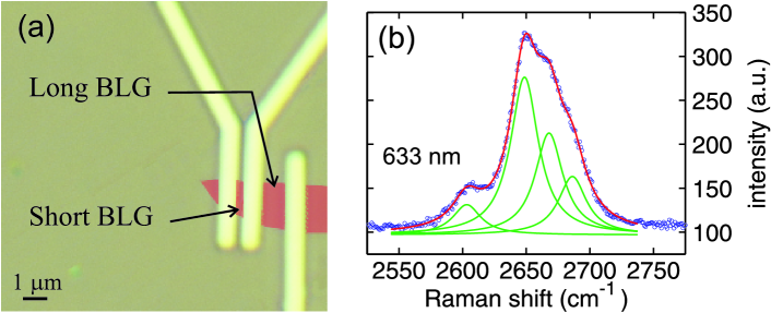
We have measured seven bilayer graphene samples in a two-lead configuration and found qualitatively the same transport properties for each of them. Here we focus on the results obtained on two samples from the same BLG sheet having lengths nm and nm, and widths nm and nm, respectively (Fig. 4). The samples were contacted using Ti/Al/Ti sandwich structures with thicknesses 10 nm / 70 nm / 5 nm (10 nm of Ti is the contact layer). Three 0.6 m wide contacts were patterned using e-beam lithography. The strongly doped Si substrate was used as a back-gate, separated by 270 nm of SiO2 from the sample.
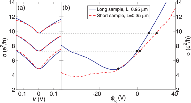
The curve of our 0.95 x 1.55 m2 sample at K is illustrated in Fig. 5 together with the in a typical MLG sample. While the MLG result is linear,meric08 ; barreiro09 the BLG curve exhibits clearly superlinear behavior at small drain-source voltage ; the nonlinearity in BLG depends relatively weakly on the gate voltage but is largest near the CNP. The nonlinear behavior can be observed more clearly in Fig. 6(a) which displays the differential conductivity of the long and short samples at a few values of . It is seen that also the length dependence of the nonlinearity at bias voltages below V is weak. This supports its interpretation as a heating effect: as mentioned above, the temperature should scale with and not, for example, the electric field . Note, furthermore, that the curves are very symmetrical.
Figure 6(b) shows the full gate voltage dependence of the zero-bias conductivity of the short and long samples. In both samples, the minimal conductivity is located in the negative gate voltage region around -10 V. The minimum zero-bias conductivities are roughly and for the short and long sample, respectively. These are close to the value typically found for both MLG and BLG.geim07 ; morozov08 An asymmetry between the -doped and -doped regions is clearly visible and is more pronounced for the short sample where the conductivity is almost constant in the -region. We interpret this electron-hole asymmetry as a sign of the leads doping the graphene,huard08 ; khomyakov10 so that there are - junctions present at larger negative gate voltages. This is consistent with expectations for Ti/Al electrodes.huard08 ; khomyakov10 In a parallel-plate approximation the charge density is , where F/m2. Using this we estimate from the slope of vs. for the long sample the mobility to be at least cm2V-1s-1. Using this the mean free path is estimated to be nm, and thus the samples are diffusive.
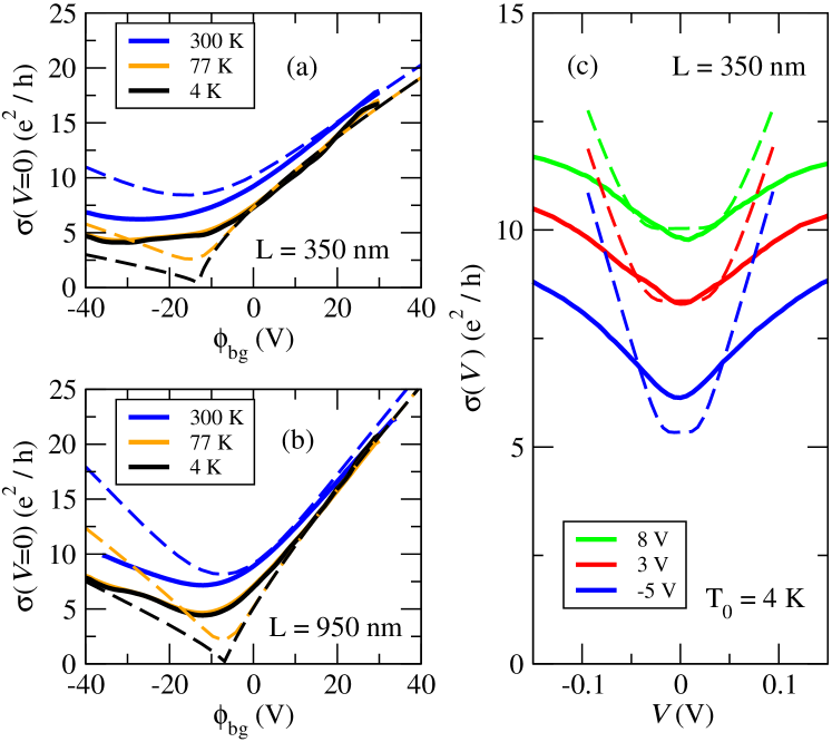
We compare the raw experimental data to the theoretical results in Fig. 7, where solid and dashed lines are for experimental and theoretical data, respectively. Figures 7(a) and (b) show the vs. dependence for the short and the long sample, respectively. Also experimental data measured at 77 K and 300 K are shown. It is seen that the zero-bias conductivity increases slightly from 4 K to 77 K, and more significantly from 77 K to 300 K. The conductivity change is strongest near the CNP and also in the -doped region. Since the theory is expected to work only in the absence of - junctions, the fitting is done only to the vs. data [Fig. 7(a,b)] at , with . The same parameters are then used for calculating . The data for the short sample are shown in Fig. 7(c).
The parameters used for the fit are given in the caption of Fig. 7. The work function mismatch eV is of the correct sign and order expected for Ti/Al electrodes.khomyakov10 A gate distance nm is used, which is smaller than the experimental nm. The smaller used for the comparison is reasonable, since in the simplified geometry assumed by the theoretical model the gate potential is more strongly screened by the transport electrodes: even for the long sample the parallel plate limit is not fully reached.footnote3 It is also notable that the average doping density – m2 is much smaller than the impurity density m2, although the simplest theories for impurity doping predict these two to be equal.adam08 Even though we model, for simplicity, the impurities to be all similar and of the screened-Coulomb type (App. B), in reality there may be several different types of disorderxiao10 present in our samples, which complicates the situation. The orders of magnitude – m2, are still in the range that can be expected from other experiments.morozov08 ; xiao10
The overall agreement of the theory with the experiment is good, apart from the large deviations for , where some parts of the system are close to the CNP. At these gate voltages the low-temperature theoretical results for tend to fall well below the experimental ones, whereas at 300 K the opposite is true. In addition to this the clearest discrepancy is that the self-heating predicted by the theory is too strong, as shown by the overly steep slope of in Fig. 7(c). Also, the slight decrease of the experimental slope with voltage is not captured. A proper explanation of these effects would require considering interactions of the electrons with phonons, particularly the remote interface phonons of the SiO2 substrate.viljas10mod ; footnote2 Another clear deviation is that the theoretical curves for high tend to be flatter close to than in the experiments. (The theoretical results for the long sample are otherwise similar as in Fig. 7(c), but even slightly more “flat”.) As suggested in Sec. II, the correct shape could presumably be reproduced by considering charge puddles, i.e., a non-uniform impurity density and doping. To keep the model simple and the number of fitting parameters small, we have neglected puddles here.
It should be noted the gross features of the results can be understood simply based on the temperature-dependence of the local conductivity,adam08 which may be worked out analytically [Eq. (9) below] and the fact that the average temperature increases roughly linearly with the bias voltage. However, the precise shape of the nonlinearity is dependent on the various sources of nonuniformity.
IV Discussion
The heating effects described above are not the only possible sources of nonlinearity. As already mentioned, at high enough bias voltage electron scattering from phonons tends to reduce the conductivity, which is expected to make the current-voltage curves at high bias sublinear. This has been seen in MLG as a tendency for the current to almost saturate.meric08 ; barreiro09 We also see similar effects in our experimentsfay09v1 with BLG at voltages V.
The possibility of nonlinear s in graphene at low bias have also been discussed based on simple arguments involving the energy-dependence of the number of open transport channels in the Landauer-Büttiker description of the linear-response conductivity.blanter07 ; sonin08 ; fay09v1 Such calculations are problematic for the prediction of current-voltage characteristics beyond linear response, however, since they do not consider the role of the actual voltage profiles.blanter07 Ideally, the electrostatic potential drop should be calculated self consistently, as we have done above.
Other mechanisms for nonlinear (mostly superlinear) current-voltage responses in graphene have very recently been discussed by many authors.vandecasteele10 ; dora10 ; rosenstein10 ; wangzheng10 ; zhou10 ; joung10 ; bistritzer10 In particular, Zener-Klein tunneling in MLG has been shown to give rise to superlinearities close to CNP.vandecasteele10 ; dora10 ; rosenstein10 It seems unlikely, however, that a similar mechanism would be of importance in our experiments, since the nonlinearity is weakly gate-dependent. Other possibilities for nonlinearities include the presence of tunnel junctionswangzheng10 or contact phenomena,zhou10 but we can disregard them as an explanation of our measurements due to the weak length-dependence of the nonlinear conductivity . Furthermore, nonlinear current-voltage curves in graphene oxides have been explained with space-charge limited currents,joung10 but such effects are likely to be negligible in metallic graphene, as also supported by the absence of any bias-doping effects in our simulations. Nonlinearities are predicted also for vertical transport in misaligned BLG or few-layer systems.bistritzer10 However, of all these possibilities the self-heating scenario presented above seems to be the most likely explanation of our experimental results.
To summarize, we have shown how Joule heating can contribute to the shape of the observed current-voltage characteristics of bilayer graphene in the diffusive limit. The heating is signified by a strong superlinear contribution in and thus a low-bias differential conductivity increasing with . Our experimental results and our numerical calculations are in good overall agreement for bias voltages V. The heating effect is much stronger in bilayer graphene than in monolayer, as can be expected from the differences in their electronic structures.
Acknowledgements.
We thank R. Danneau, M. Y. Tomi, J. Wengler, F. Wu, and R. Hänninen for fruitful discussions. This work was supported by the Academy of Finland, the European Science Foundation (ESF) under the EUROCORES Programme EuroGRAPHENE, and the CIMO exchange grant KM-07-4656 (MW).Appendix A Green function and characteristic functions
The Green function of the Laplace operator satisfies , and zero boundary conditions on the electrodes. For the particular geometry under consideration (Fig. 1) the Green function may be found analytically using conformal mapping techniques and it is
| (3) |
where , and so on.
The characteristic function for electrode is defined such that it satisfies the Laplace equation with the boundary condition that on electrode and on the other electrodes. Once the Green function is known, the characteristic functions may be easily represented in terms of it:
| (4) |
Appendix B Charge concentration and transport coefficients for graphene
In our semiclassical model the charge density is assumed to be of the form
| (5) |
where is the Fermi function, , and we define , where is the density of states (DOS). Using Eq. (5) self consistently in the Poisson equation is essentially the Thomas-Fermi approximation.khomyakov10
Assuming a diffusive system with only elastic impurity scattering the transport coefficients are given by
| (6) |
with . Here is the thermal broadening function, and we define , where is the energy-dependent Boltzmann conductivity. The quantity the diffusion constant, where is the group velocity and the transport relaxation time.
It is easy to see by change of the integration variable that the quantities in Eqs. (5) and (6) only depend on the difference . Thus below we define the “hatted” quantities with , , and similarly for the other transport coefficients.
As a specific model for the impurity scattering we consider only screened Coulomb impurities, which lead to a linear dependence of the conductivity on charge densityadam08 for both BLG and MLG, as observed in most experiments.morozov08 (For BLG also short-range scattering may be of importance.xiao10 ) For simplicity we assume all of the bare impurities to carry a charge and to be at zero distance from the graphene, and perform an average with respect to their positions.adam08 For BLG and MLG some further approximations are made, as explained below.
B.1 Bilayer graphene
For BLG we assume a purely parabolic and gapless dispersion , where m/s and eV. This yields a group velocity and a constant DOS . Then
| (7) |
The DOS leads to an inverse Thomas-Fermi screening length nm-1.
For the charged impurity scattering we use the “complete-screening” approximation.adam08 Thus we find , where is the average impurity density. This yields
| (8) |
Then the transport coefficients are
| (9) |
where is the Lorenz number. Here and is the dilogarithm function.nistbook and is defined as
| (10) |
This function has the limits , when , and , when . Using these we see that the Wiedemann-Franz law only applies if .
B.2 Monolayer graphene
For MLG the dispersion relation is , giving a constant group velocity m/s, and a density of states . Then
| (11) |
Here we have defined the function , which has the limits , when , and , when . The inverse screening length is now , with .
For the impurity scattering we now assume that the “effective fine-structure constant” adam07b ; adam08 of MLG is small, 1. (For SiO2 , and .) In this way we find . These give
| (12) |
The transport coefficients are thus
| (13) |
Note again that the Wiedemann-Franz law is only approximately valid in the limit .
Appendix C Low-bias resistance of - junction: classical thermal activation vs. quantum tunneling
In order to understand the temperature-dependence of the conductivity in Fig. 2 at , we discuss some analytical results for the semiclassical conductance of a - junction in BLG or MLG. The existence of a - junction at location means that . At low temperature we linearize around this point, such that , where . The classical linear-response conductance for width is then , where .
C.1 BLG
In this case is given by Eq. (9). Since we use the parabolic-band approximation, the integral diverges logarithmically and a cutoff length is needed, which should be on the order of . In this way, the conductance of a - junction (width ) may be approximated with
| (14) |
The temperature-dependence has a logarithmic singularity at . This is the behavior seen in Fig. 2(a) at .
Clearly the semiclassical result must break down at low enough temperature, in which case some quantum-mechanical result taking into account Zener-Klein tunneling is needed. The zero-temperature conductance would then remain finite. The simplest way to approximate the crossover temperature is to use a Wenzel-Kramers-Brillouin (WKB) approximation in a similar fashion as done for MLG.cheianov06 ; sonin09 ; vandecasteele10 Estimates of this type show that the crossover temperature may well be on the order of room temperature. We note that such a calculation predicts a superlinear current with , unlike in MLG where .
C.2 MLG
Here is found from Eq. (13). The - junction in MLG has a conductance
| (15) |
The linear temperature dependence is seen in Fig. 2(c) at . At low temperature the junctions completely dominate the conductivity of the entire sample. However, again, at low enough temperature this result breaks down. WKB estimates shows that this may occur already close to room temperature. Thus the Boltzmann calculations are only valid in the absence of - junctions.
References
- (1) A. H. Castro Neto, F. Guinea, N. M. R. Peres, K. S. Novoselov, and A. K. Geim, Rev. Mod. Phys. 81, 109 (2009)
- (2) S. Das Sarma, S. Adam, E. H. Hwang, and E. Rossi, “Electronic transport in two dimensional graphene,” (2010), arXiv:1003.4731
- (3) S. Adam, E. H. H. amd V. M. Galitski, and S. D. Sarma, Proc. Natl. Acad. Sci. 104, 18392 (2007)
- (4) S. V. Morozov, K. S. Novoselov, M. I. Katsnelson, F. Schedin, D. C. Elias, J. A. Jaszczak, and A. K. Geim, Phys. Rev. Lett. 100, 016602 (2008)
- (5) S. Adam and S. Das Sarma, Phys. Rev. B 77, 115436 (2008)
- (6) S. Xiao, J.-H. Chen, S. Adam, E. D. Williams, and M. S. Fuhrer, Phys. Rev. B 82, 041406 (2010)
- (7) S. Adam and M. D. Stiles, Phys. Rev. B 82, 075423 (2010)
- (8) S. Das Sarma, E. H. Hwang, and E. Rossi, Phys. Rev. B 81, 161407 (2010)
- (9) I. Meric, M. Y. Han, A. F. Young, B. Ozyilmaz, P. Kim, and K. L. Shepard, Nature Nanotechnol. 3, 654 (2008)
- (10) A. Barreiro, M. Lazzeri, J. Moser, F. Mauri, and A. Bachtold, Phys. Rev. Lett. 103, 076601 (2009)
- (11) N. Vandecasteele, A. Barreiro, M. Lazzeri, A. Bachtold, and F. Mauri, Phys. Rev. B 82, 045416 (2010)
- (12) B. Huard, N. Stander, J. A. Sulpizio, and D. Goldhaber-Gordon, Phys. Rev. B 78, 121402 (2008)
- (13) S. Barraza-Lopez, M. Vanević, M. Kindermann, and M. Y. Chou, Phys. Rev. Lett. 104, 076807 (Feb 2010)
- (14) P. A. Khomyakov, A. A. Starikov, G. Brocks, and P. J. Kelly, Phys. Rev. B 82, 115437 (2010)
- (15) J. K. Viljas and T. T. Heikkilä, phys. Rev. B 81, 245404 (2010); Note that the results in Fig. 3(c) and 3(d) of this reference are too large by factor of four — this has no essential effect on the other results.
- (16) J. Martin, N. Akerman, G. Ulbricht, T. Lohmann, J. H. Smet, K. von Klitzing, and A. Yacoby, Nature Phys. 4, 144 (2008)
- (17) A. Deshpande, W. Bao, Z. Zhao, C. N. Lau, and B. J. LeRoy, Appl. Phys. Lett. 95, 243502 (2009)
- (18) A simple way of taking phonons into account would be to subtract the power lost to them in the heat balance. The magnitudes of the electron-phonon power for various types of phonons have been estimated in Ref. viljas10mod, . For example the power per area for optical phonons of energy is of the form where and we assume that the phonons do not heat above . Considering the remote phonons of a SiO2 substrate we may use meV and then mW/m2, which appears to be of the right order for reducing the slope of . However, such a procedure cools long samples more effectively, making length dependent. For a proper description, the heating of the phonons and the modification of the transport coefficients should be accounted for.
- (19) V. B. Shikin, Phys. Rev. B 64, 245335 (2001)
- (20) A. C. Ferrari, J. C. Meyer, V. Scardaci, C. Casiraghi, M. Lazzeri, F. Mauri, S. Piscanec, D. Jiang, K. S. Novoselov, S. Roth, and A. K. Geim, Phys. Rev. Lett. 97, 187401 (Oct 2006)
- (21) A. K. Geim and K. S. Novoselov, Nature Materials 6, 183 (2007)
- (22) The use of nm may not be justified for the long sample. However, the data for it could also be fitted with the correct and a somewhat smaller , which is another unknown parameter that can vary between the samples.
- (23) A. Fay, J. K. Viljas, R. Danneau, F. Wu, M. Y. Tomi, J. Wengler, M. Wiesner, and P. J. Hakonen, arXiv:0904.4446v1 (unpublished)
- (24) Y. M. Blanter and I. Martin, Phys. Rev. B 76, 155433 (Oct 2007)
- (25) E. B. Sonin, Phys. Rev. B 77, 233408 (2008)
- (26) B. Dóra and R. Moessner, Phys. Rev. B 81, 165431 (2010)
- (27) B. Rosenstein, M. Lewkowicz, H. C. Kao, and Y. Korniyenko, Phys. Rev. B 81, 041416 (2010)
- (28) H. M. Wang, Z. Zheng, Y. Y. Wang, J. J. Qiu, Z. B. Guo, Z. X. Shen, and T. Yu, Appl. Phys. Lett. 96, 023106 (2010)
- (29) Y.-B. Zhou, B.-H. Han, Z.-M. Liao, Q. Zhao, J. Xu, and D.-P. Yu, J. Chem. Phys. 132, 024706 (2010)
- (30) D. Joung, A. Chunder, L. Zhai, and S. I. Khondaker, Appl. Phys. Lett. 97, 093105 (2010)
- (31) R. Bistritzer and A. H. MacDonald, Phys. Rev. B 81, 245412 (2010)
- (32) NIST Handbook of Mathematical Functions, edited by F. W. J. Olver, D. W. Lozier, R. F. Boisvert, and C. W. Clark (National Instiute of Standards and Technoogy, and Cambridge University Press, Cambridge, 2010)
- (33) V. V. Cheianov and V. I. Fal’ko, Phys. Rev. B 74, 041403 (2006)
- (34) E. B. Sonin, Phys. Rev. B 79, 195438 (2009)