Spin-Polarized to Valley-Polarized Transition in Graphene Bilayers at in High Magnetic Fields
Abstract
We investigate the transverse electric field () dependence of the =0 quantum Hall state (QHS) in dual-gated graphene bilayers in high magnetic fields. The longitudinal resistivity () measured at =0 shows an insulating behavior which is strongest in the vicinity of =0, and at large -fields. At a fixed perpendicular magnetic field (), the =0 QHS undergoes a transition as a function of , marked by a minimum, temperature-independent . This observation is explained by a transition from a spin polarized =0 QHS at small -fields, to a valley (layer) polarized =0 QHS at large -fields. The -field value at which the transition occurs has a linear dependence on .
pacs:
73.21.-b,73.22.Gk,73.43.-fGraphene bilayers novoselov_natphys06 represent an attractive system for electron physics, and potential device application. This system exhibits a transverse electric field tunable band-gap mccannprl06 ; min , as evidenced by angle-resolved photoemission ohta and transport measurements castro07 ; oostinga . In a perpendicular magnetic field, graphene bilayers show quantum Hall states at integer filling factors () multiple of four novoselov_natphys06 ; castro07 , owing to spin and valley degeneracy. Electron-electron interaction can lift the Landau level (LL) spin and valley degeneracy barlas , leading to broken symmetry quantum Hall states experimentally observed in single-gated suspended feldman09 , and supported zhao10 graphene bilayers.
We investigate dual-gated graphene bilayers, a device geometry which allows independent control of the total density and transverse electric field. At a fixed perpendicular magnetic field (), we observe the emergence of a quantum Hall state (QHS) at filling factor in the presence of a transverse electric field (), evinced by a large longitudinal resistivity () with an insulating behavior, consistent with the opening of a gap between the electron and hole bands. Interestingly, as the -field is increased we observe a developing QHS at =0, explained by the Zeeman splitting of the Landau levels at zero energy. As a function of , the QHS undergoes a transition from spin polarized at small -fields, to valley (layer) polarized at large -fields.
Our samples consist of natural graphite mechanically exfoliated on a 300 nm SiO2 dielectric layer, thermally grown on a highly doped -type Si substrate, with an As doping concentration of cm-3. Optical inspection and Raman spectroscopy are used to identify graphene bilayer flakes for device fabrication. We define metal contacts using electron beam (e-beam) lithography followed by 50 nm Ni deposition and lift-off [Fig. 1(a)]. A second e-beam lithography step followed by O2 plasma etching are used to pattern a Hall bar on the graphene bilayer flake. To deposit the top gate dielectric, we first deposit a thin Al layer as a nucleation layer for the atomic layer deposition (ALD) of Al2O3. The sample is then transferred ex-situ to an ALD chamber. X-ray photoelectron spectroscopy and electrical measurements confirm the Al layer is fully oxidized in the presence of residual O2 during evaporation, and the exposure to ambient O2 dignam . Next, a 15 nm-thick Al2O3 film is deposited using trimethyl aluminum as the Al source and H2O as oxidizer kim , followed by the Ni top gate deposition [Fig. 1(a)]. Longitudinal () and Hall () resistivity measurements are performed down to a temperature of K, and using standard low-current, low-frequency lock-in techniques. Three samples, labeled as A, B, and C, with mobilities of cm2/Vs were investigated in this study, all with similar results.
We use Hall measurements to determine the total carrier density () as a function of top () and back () gate voltages, and the corresponding capacitance values. Equally relevant here is the transverse electric field, which induces an imbalance between the bottom () and top () layer densities. Up to an additive constant, and are related to and by , and ; is the electron charge, is the vacuum dielectric permitivity Efield . The values for our samples range between 225 - 270 nF/cm2, with a dielectric constant =4.2 - 5.
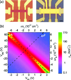
In Fig. 1(b) we show measured as a function of and in sample A, at K. The diagonals of constant represent the loci of constant and varying , while diagonals of constant define the loci of constant at varying . The diagonal of is defined by the points of maximum measured as a function of at fixed values. In order to determine the and values at which and , we consider measured along the diagonal . The shows a minimum and increases markedly on both sides, thanks to the transverse electric field induced band-gap opening mccannprl06 ; mccann ; min ; oostinga . The minimum on the diagonal defines the point. Having established a correspondence between (, ) and (, ), in the reminder we characterize the bilayers in terms of and .
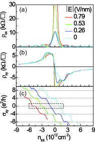
In Fig. 2(a,b) we show vs. and vs. respectively, measured at fixed -field values, at T and K in sample A. These data are measured by simultaneously sweeping and , such that remains constant. The data show QHSs, marked by vanishing at integer filling factors multiple of four, consistent with the four-fold degeneracy associated with spin and valley of each Landau level novoselov_natphys06 ; mccannprl06 ; mccann . Using the measured and , we determine the Hall conductivity () via a tensor inversion, . Figure 2(c) data show vs. , measured at T and K, and for different values of . Figure 2(a) data show an increasing at with increasing , translating into a Hall conductivity plateau at [Fig. 2(c)], which signals a developing QHS at at large .
The QHS in graphene bilayers at high -fields is explained as follows. In an applied perpendicular -field the energy spectrum consists of the four-fold, spin and valley degenerate Landau levels (LLs). At an eight-fold degenerate LL, i.e. the spin and valley degenerate and LLs mccannprl06 ; mccann , exists at energy , the electron-hole symmetry point. The , and LL wave-functions are layer polarized mccannprl06 ; mccann , and can be indexed by the layer degree of freedom, in addition to spin. In an applied transverse -field the eight-fold degenerate LL at splits into two, four-fold degenerate LLs, separated the same energy gap () mccannprl06 ; mccann , which exists between the electron and hole bands at . The higher (lower) energy LLs correspond to the spin degenerate and LLs residing in the layer with higher (lower) on-site energy.
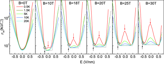
Figure 3 data show vs. measured at different values, at . The data is collected by sweeping and in opposite directions, with sweep rates proportional to , and , respectively. At , the shows a nearly exponential increase with , combined with an insulating behavior, a consequence of the -field induced band-gap opening. The -dependence of the is weaker than the exponential expected for a band insulator, and instead follows more closely a dependence, attributed to variable range hopping between disorder-induced states in the gap zou ; taychatanapat . In a perpendicular magnetic field, the vs. data also show an exponential divergence at finite values, consistent with the -field induced splitting of the LLs. However, a closer examination of the vs. data in high -fields reveals an interesting trend. Let us first consider Fig. 3 data collected at the highest temperature, K. Unlike the case, the onset of the divergence occurs at a finite -field, which also increases with , indicating the -field induced LL splitting is suppressed for small transverse -fields. This observation is a direct consequence of the and LLs being layer polarized. Let us assume the transverse -field is applied such that the on-site energy of electrons of the top layer is higher than that on the bottom layer. At filling factor the and LLs of the bottom layer will be fully occupied, while the and LLs of the top layer will be empty. Such LL occupancy will innately place more electrons in the bottom layer, setting up an internal electric field which opposes the externally applied -field. The magnitude of the internal electric field is related to the LL degeneracy as
| (1) |
Further examination of Fig. 3 data reveals another interesting finding. In high -fields, shows an insulating state centered at , which becomes more pronounced with increasing the -field. This signals a splitting of the LLs, and consequently a developing QHS at , which is attributed to the spin splitting of the and LLs. As the -field increases decreases, and the insulating state weakens. At a fixed -field, the vs. data show a temperature independent minimum at a critical field . For fields higher than , the shows a diverging dependence on , a consequence of the -field induced splitting of the and LLs. The -field marks a transition at , from a spin polarized QHS at small -fields to a valley (layer) polarized QHS at large -fields, in agreement with several recent theoretical studies which examined the phase diagram as a function of transverse -field, and considering the electron-electron interaction gorbar10 ; nandkishore ; toke10 . We remark that the vs. data of Fig. 3 are symmetric for both negative and positive -fields, which indicates the the disorder is similar for the two layers.
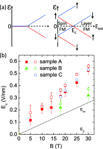
Figure 4(a) shows qualitatively the expected dependence of the and LL energies on the -field. In the absence of spin splitting [Fig. 4(a), left panel], the LL layer degree of freedom remains degenerate at finite -field, owing to the LL layer polarization. In the presence of spin splitting [Fig. 4(a), right panel], the spin down LLs of both layers are occupied, while the spin up LLs are empty. An applied -field increases (reduces) the energy of the top (bottom) layer LLs, which cross at a field . Figure 4(b) data summarizes the vs data measured for three samples, marked by different symbols. We employ two criteria to define using Fig. 3 data. The open symbols in Fig. 4(b) indicate the onset of the divergence at high fields, shown as a black arrows in Fig. 3. The closed symbols in Fig. 4(b) represent the -fields at which is temperature independent, and are marked by circles in Fig. 3. Both criteria yield similar values, with slightly higher values for the first criterion. It is instructive to compare the the experimental values with two simple calculations. The first is the electric field () required to split the LLs when the layer polarization is taken into account [Eq. (1)]. The second is the electric field at which the electron Zeeman energy () is equal to the on-site energy difference between the layers:
| (2) |
The values calculated assuming a -factor of 2, and an inter-layer distance Å are represented by the dotted trace in Fig. 4(b); is the Bohr magneton. Neglecting interaction, the QHS undergoes a transition from spin to valley polarized at an -field equal to . Examination of Fig. 4 data shows that is much larger than , and comparable albeit larger than .
We discuss the role of Zeeman splitting on the spin to valley polarized transition. Using vs. at different -fields, measured at a 48∘ angle between the normal to the sample plane and the magnetic field, we extracted a set of vs. values similar to Fig. 4(b) data, but with a 1.5 times larger Zeeman splitting. We find that the values remain independent of the in-plane component of the magnetic field, and are determined only by the -field perpendicular to the sample. Lastly, we address the role of the edge states. A subtle issue with exfoliated bilayers is the two layers may not necessarily terminate at the same position, leading to single layer edge states in high magnetic fields. To test if the edge termination affects Figs. 3 and 4 data, we probed both as exfoliated samples (A), and samples (B,C) where an O2 plasma etch was used to pattern Hall bars, where both layers terminate at the same position.
Several theoretical studies have examined the spin to valley polarized transition in graphene bilayers at . Gorbar et al. gorbar10 predict a first order phase transition from spin to valley polarized at an -field of 1 mV/nm[T]. A similar linear vs. dependence is found in two other studies nandkishore ; toke10 , but with at a larger field, of 9 mV/nm[T]. Tőke and Fal’ko toke10 suggest an intermediate, compressible phase between the spin and valley polarized QHSs, with the spin polarized phase collapsing at relatively small electric fields. Figure 3 data show that the spin polarized phase remains gapped at all fields except for in the vicinity of .
A closely similar system to the QHS in graphene bilayers, is the QHS in double layer GaAs/AlGaAs heterostructures sawada . Depending on the balance between the Zeeman energy, on-site layer energy difference (), and the tunneling energy (), the QHS can be either spin or layer polarized, with an intermediate canted spin phase brey ; macdonald . The Hartree-Fock theory of the QHS macdonald shows a first-order transition from spin to layer polarized when the exchange energy equals the direct (Hartree) energy, a limit reached when is much smaller than the magnetic length (). The is satisfied up to the highest magnetic fields here, as at T, rendering the QHS in graphene A-B bilayers equivalent with the QHS in double quantum wells, in the limit of zero tunneling (), and small Zeeman energy (). Interestingly, the limit in GaAs double quantum wells cannot be reached because of limitations associated finite well and barrier widths, finite tunneling, and carrier density.
A recent study of dual-gated, suspended graphene bilayers weitz reports a similar transition at as a function of transverse electric field, but probed at much lower -fields and up to T. Although the sample mobilities, and the range of -fields and magnetic fields explored in Ref. weitz are very different, remarkably the linear vs. dependence is in good agreement with the results of this study.
In summary, the QHS in dual-gated graphene bilayers in high magnetic field reveals two regimes: at , as a result of the spin splitting, and at large -fields when the system is layer polarized. The QHS undergoes a transition from spin to valley (layer) polarized at a critical electric field (), which depends linearly on , with a slope of 12-18mV/nmT-1. Our data, interpreted in the framework of existing theories, suggest the exchange and direct energies are comparable at .
We thank A. H. MacDonald, E. V. Castro, D. Tilahun, S. K. Banerjee, I. Jo, and J. H. Seol for many discussions and experimental support. We acknowledge NRI and NSF (DMR–0819860) for financial support. Part of our work was performed at the National High Magnetic Field Laboratory, which is supported by NSF (DMR–0654118), the State of Florida, and the DOE.
References
- (1) K. S. Novoselov et al., Nature Phys. 2, 177 (2006).
- (2) E. McCann and V. I. Fal’ko, Phys. Rev. Lett. 96, 086805 (2006).
- (3) H. Min et al., Phys. Rev. B75, 155115 (2007).
- (4) T. Ohta et al., Science 313, 951 (2006).
- (5) E. V. Castro et al., Phys. Rev. Lett. 99, 216802 (2007).
- (6) J. B. Oostinga et al., Nature Mat. 7, 151 (2008).
- (7) Y. Barlas et al., Phys. Rev. Lett. 101, 097601 (2008).
- (8) B. Feldman, J. Martin, and A. Yacoby, Nat. Phys. 5, 889 (2009).
- (9) Y. Zhao et al., Phys. Rev. Lett. 104, 066801 (2010).
- (10) M. J. Dignam, W. R. Fawcett, H. Bohni, J. Electrochem Soc. 113, 656 (1966).
- (11) S. Kim et al., Appl. Phys. Lett. 94, 062107 (2009).
- (12) To calculate the -field we offset and by the gate biases required to reach and .
- (13) E. McCann, Phys. Rev. B74, 161403(R) (2006).
- (14) K. Zou and J. Zhu, Phys. Rev. B82, 081407(R) (2010).
- (15) T. Taychatanapat and P. Jarillo-Herrero, Phys. Rev. Lett. 105, 166601 (2010).
- (16) E. V. Gorbar, V. P. Gusynin, and V. A. Miransky, Phys. Rev. B81, 155451 (2010).
- (17) R. Nandkishore and L. S. Levitov, arXiv:1002.1966 (2010).
- (18) C. Tőke and V. I. Fal’ko, Phys. Rev. B83, 115455 (2011).
- (19) A. Sawada et al., Phys. Rev. Lett. 80, 4534 (1998).
- (20) L. Brey et al., Phys. Rev. Lett. 83, 168 (1999).
- (21) A. H. MacDonald et al., Phys. Rev. B60, 8817 (1999).
- (22) R. T. Wietz et al., Science 330, 812 (2010).