A Sawtooth Permanent Magnetic Lattice for Ultracold Atoms and BECs
Abstract
We propose a new permanent magnetic lattice for creating periodic arrays of Ioffe-Pritchard permanent magnetic microtraps for holding and controlling ultracold atoms and Bose-Einstein condensates (BECs). Lattice can be designed on thin layer of magnetic films such as . In details, we investigate single layer and two crossed layers of sawtooth magnetic patterns with thicknesses of 50 and 500nm respectively with a periodicity of 1m. Trap depth and frequencies can be changed via an applied bias field to handle tunneling rates between lattice sites. We present analytical expressions and using numerical calculations show that this lattice has non-zero potential minima to avoid majorana spin flips. One advantage of this lattice over previous ones is that it is easier to manufacture.
pacs:
67.85.Hj,67.85.Jk,37.10.Gh,37.10.De,85.85.+j1 Introduction
Focused laser beams have been used extensively in years for cooling atoms and molecules
to hold them h.p-02 ; rmp-98 ; prl-01 ; prl-98 ; Oc-75 . These optical traps are made by a radiation field whose intensity has a
maximum in space. Due to interaction with electric field of laser, small clouds of atoms can
be confined, manipulated and controlled in optical lattices epj-05 ; prl-98-2 ; arx-428 . Radiation absorption and induced
dipole forces constrain atoms to optical lattice p-s-08 . Periodic optical lattices are the result of
interference of intersecting laser beams and have allowed for the observation of the Mott-insulator
to superfluid transition pra-10 ; nat-02 , studies of low-dimensional and quantum degenerate
gases prl-06 ; prl-08 and coherent molecules p . In quantum computation, optical lattices provide
a large qubit system and produce gate operations on the register n.o-08 ; lpr-07 .
Using magnetic field is another approach to realize harmonic potential in space prl-98-4 .
Magnetic lattices are created using periodically magnetized films or current
carrying wires on atom chips jpb-06 ; jpb-07 ; prl-99 ; prl-99-2 ; epj-05-2 . These magnetic potentials are promising alternatives to the optical
lattices and provide a high degree of design flexibility, arbitrary geometries and lattice
spacing. Magnetic lattices can produce highly stable periodic potential wells with low noise rmp-07 . Single 3D magnetic microtraps also have been introduced either by current carrying wires or
permanent magnetic slabs pra-09 ; arx-10 . Recently, development of technology has let us for working
on high-quality magnetic materials based on permanent, perpendicularly magnetized films pra-08 ; pra-07 . Periodic grooved magnetic mirrors have been made by the technology of thin films to
reflect ultracold atoms pra-09-2 . In the presence of magnetic bias fields, mirrors are transferred into
1D arrays of 2D waveguides and 2D arrays of 3D traps jpb-06 . Magnetic films such as
have excellent magnetic properties; homogeneity, high magnetization, large coercivity (3k) and high Curie temperature(300oC) jpb-06 ; jpb-07 .
In this paper, we introduce a new atom chip based on permanent periodic grooved magnetic
film and external magnetic fields. This sawtooth magnetic lattice is proposed for
controlling, manipulating and trapping clouds of ultracold atoms when they are in low-field
seeking states. Analytical expressions and numerical calculations show that the magnetic field minima are non-zero. Therefore, ultracold atoms
can be hold and trapped without any spin flips in lattice sites. In particular, we investigate 1D
array of this grooved magnetic lattice, when bias fields are applied. Results show that
produced waveguides have controllable depth and frequencies to handle clouds of quantum
degenerate gases on the chip surface. We show that two crossed separated layers of periodic
arrays also can produce 2D magnetic lattice of 3D microtraps when bias fields are applied.
The microtraps have non-zero minimum and high depth (0.2mK) which cause
prevention of majorana spin flips and efficient restriction of trapped atoms, respectively.
Magnetic atom chips based on permanent magnetic materials have some advantages over
optical or microwire devices. Since there is no spontaneous emission due to decay of excited
atoms, light scattering and decoherence of cold atoms vanishes and no beam alignment is
required p-s-08 . Heat dissipation and loss of atoms due to fluctuation of current in current-carrying
microwires are prevented in permanent magnetic lattices. They can produce large field
curvatures, large trap depth and high frequencies with very low technical noises rmp-07 . the Main
motivation of this work is introducing a more flexible permanent magnetic lattice compared with the configuration of the two crossed arrays of rectangular permanent magnetic slabs proposed in jpb-06 . Considering the shape of this new atom chip, current technology in grooving of films for magnetic
mirrors allows us to produce it more easily compared with previous ones.
2 Analytical expressions for Magnetic lattices
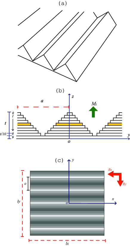
We study first the simple case of a single layer of sawtooth periodic array of grooved magnetic films with a thickness of , periodicity along the -direction, magnetization = and constant bias magnetic fields , and along the -, - and -directions.
2.1 Atom waveguide
The configuration of the permanent magnets is shown in Fig.1. Pattern of magnetic film has a periodicity (distance between two alternative peaks) of m and a thickness of nm while dimensions of lattice in - and - directions, and are 1mm (Fig.1(c)). For analytical and numerical calculations, we approximate our sawtooth magnetic pattern thin rectangular magnetic slabs same magnetization and periodicity but with different widths. As Fig.1 (a) shows, infinite periodic arrays of magnets are placed above each other to shape sawtooth structure. At a large distance where ()1, the using expressions given in Ref. jpb-06 , the components of the magnetic field can be written
| (1) | |||||
where =2 and , respectively. and are /(Gaussian units) and related coefficient of the th infinite periodic magnets on atom chip [see Fig.1(b)], respectively. is determined from the series [for more details, see section 2.3]
| (2) | |||||
where is the number of sub-layers (i.e. order of approximation). The magnitude of the magnetic field above surface can be written
In simple case when we take =0, the minimum of magnetic field in 1D array of periodic magnetic lattice of 2D microtraps is
| (4) |
where the center of the waveguides are located at
| (5) | |||||
where is the trap number in the -direction and takes values of 0, 1, 2,… .
According to equation 4, the component of the bias field is necessary to avoid spin flips near the center of 2D microtraps.
The magnetic barrier heights along - and -directions which depend on the bias fields are given by
| (6) | |||||
Second derivatives (curvatures) of the magnetic field at the minimum of the potential and trap frequencies of the waveguides along - and -directions could be analytically determined by
| (7) | |||||
| (8) |
where , , and are the Bohr magneton, Lande factor, magnetic quantum number and mass of atom, respectively. Equations (5) and (8) show that increasing reduces and increases frequencies of the traps, respectively. The frequencies of traps are independent of magnetization of the magnetic film. They depend on the external magnetic fields and the periodicity of magnetic lattice.
2.2 2D permanent magnetic lattice of microtraps
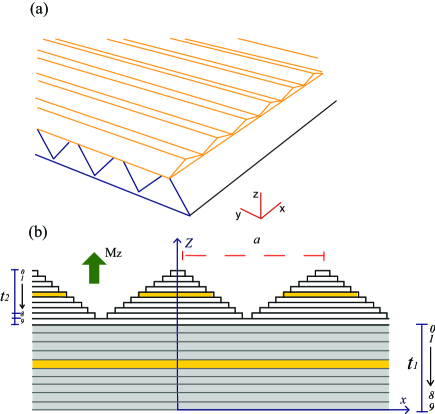
In order to produce Ioffe-Pritchard microtraps, two crossed layers of periodic arrays of sawtooth magnetic films with two different thicknesses of and , separation of and same magnetization with uniform bias fields is investigated (Fig.2). The top and bottom arrays have same periodicity along - and -directions. Thickness of bottom array, is larger than thickness of top array, . is along z-direction and bias fields are and . The components of the magnetic field, for the large distances (k(z--)1) from top of the surface can be obtained by
| (9) | |||||
where . Coefficient of the th sublayer of infinite magnets of the top array, is determined, similary
where is the gap between bottom and top arrays. The magnitude of magnetic field above the surface can be written
| (11) |
Non-zero minimum of the magnetic field and the center of microtraps in -,- and z-directions for =0 can be determined by
| (12) | |||||
| (13) | |||||
where and are number of microtraps and take 0, 1, 2,… values. Dimensionless constant is (1/2)(1+1/ where . At the center of 3D microtraps, the curvature of magnetic fields and barrier heights can be obtained by
| (14) | |||||
| (15) | |||||
where and are
| (16) | |||||
The frequencies of microtraps in three directions are
| (17) |
For a symmetrical 2D magnetic lattice, same magnetic height barriers in - and -directions, are needed. The constraint of satisfies our request where .
2.3 Corresponding magnetic coefficients of estimated layers

The components of magnetic field for infinitely long and thin permanent magnetic slabs along the -direction arranged with periodicity along the - direction and separation distance /2 between the center of neighboring slabs, are given by apb-02
where and are 2/ and (ekt-1), respectively. As we mentioned earlier in 2.1 and 2.2, permanent magnetic slabs with sawtooth geometry can be estimated by multi-layer arrays of rectangular magnets with same periodicity and different width , where is the number of a specific sublayer. The major problem is the calculation of magnetic field of sub-layers with /2 or /2. In other words, for magnetic slabs with different width and separation, Eq.18 does not work and needs to be modified. As Fig.1 (b) shows, width plus separation between neighboring slabs for each sublayer is constant and equal to periodicity of the lattice. It means that for any modification of Eq.18, remains unchanged. The new components of magnetic field for slabs with arbitrary width are related to Eq.18 by coefficient . The slabs of periodic lattice by width and separated gap /2 can be divided into narrow slabs (Fig.3) with width =/2. The magnitude of magnetic field due to these narrow slabs is related to the initial slab with coefficient . For the calculating of , narrow slabs can be shifted by small steps of /4 along axis to make initial array. The component of the magnetic field for these shifted narrow slabs, for example in -direction must be consistent with Eq.18, so we have
where is determined
| (20) |
We use these narrow slabs as unit to design any periodic lattice by arbitrary slab width and periodicity . In general, the slabs must be several times shifted to the right and left to model the given periodic array. These shifts lead to another series in calculation of the magnetic field which is given by
| (21) |
For sawtooth array, all estimated sub-layers have same thickness and distance from origin = 1-(+1)/. Summation on and for =10 sub-layers are determined 13.97 and 5.47, while for =20 sub-layers reduce to 13.02 and 5.45 values, respectively.
3 Numerical calculations for magnetic lattice
Numerical calculations for finite arrays of sawtooth magnetic films with finite length were made. Radia Package rad , interfaced to Mathematica software was used to numerically obtain magnetic field for different configurations of magnets in 1D array of waveguides and 2D arrays of 3D microtraps.
3.1 Atom waveguide
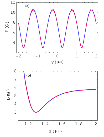
Numerical calculations of 1D array of waveguides above the sawtooth surface of the atom chip were performed when bias magnetic field along the -direction, was applied. Thickness =500nm, periodicity =1m, magnetization 4=3.8kG, finite toothy magnets number =5001 which is approximated by =10 rectangular slabs. In Fig.4, the components of magnetic field of atom chip above the surface are shown where = 5G. This configuration may be used as spatial grating to diffract slowly moving atoms. By including = 3G parallel to the waveguide axis, center of waveguides becomes non-zero with ==3G to avoid spin flips of cold atoms. Center of waveguides is at =1.29m from bottom of the layer. Magnetic barrier heights along - and -directions are 7.4 and 2.8G, respectively. The trap frequencies of 2D microtrap in - and -directions are numerically determined 236.7 kHz for 87Rb atoms. Fig.4 (a) and (b) show excellent agreement with numerical calculations and analytical expressions of magnetic field along - and -directions for /2. Numerically calculated parameters and related analytical expressions for a sawtooth magnetic film with bias fields are listed in table 1.
| Parameter | Definition | Numerical | Analytical |
|---|---|---|---|
| =10 =20 | =10 =20 | ||
n_r |
Number of magnets in -direction | 5001 | |
y_{min}(m) |
Center of first waveguide in -direction | 0.25 | 0.25 |
z_{min}(m) |
Center of waveguides in -direction | 1.29 1.28 | 1.29 1.28 |
\frac{\partial^2 B}{\partial y^2}\hspace{.1cm}({G\over{cm}^2}) |
Curvature of B in -direction | 3.291010 | 3.281010 |
\frac{\partial^2 B}{\partial z^2}\hspace{.1cm}({G\over{cm}^2}) |
Curvature of B in -direction | 3.291010 | 3.281010 |
\omega_y/2(kHz) |
Trap frequency in - direction | 231.5 | 231.5 |
\omega_z/2(kHz) |
Trap frequency in - direction | 231.5 | 231.5 |
B_{min} (G) |
Minimum of B at center of waveguides | 3 | 3 |
| Parameter | Definition | Numerical | Analytical |
|---|---|---|---|
| =10 =20 | =10 =20 | ||
n_r |
Number of magnets in - and -direction | 5001 | |
x_{min}(m) |
Center of first microtrap in -direction | 0.25 | 0.25 |
y_{min}(m) |
Center of first microtrap in -direction | 0.25 | 0.25 |
z_{min}(m) |
Center of microtrap in -direction | 1.33 1.31 | 1.33 1.31 |
\frac{\partial^2 B}{\partial x^2}\hspace{.1cm}({G\over{cm}^2}) |
Curvature of B in -direction | 2.981010 | 2.981010 |
\frac{\partial^2 B}{\partial y^2}\hspace{.1cm}({G\over{cm}^2}) |
Curvature of B in -direction | 2.981010 | 2.981010 |
\frac{\partial^2 B}{\partial z^2}\hspace{.1cm}({G\over{cm}^2}) |
Curvature of B in -direction | 5.951010 5.971010 | 5.961010 5.971010 |
\omega_x/2(kHz) |
Trap frequency in - direction | 220 220.5 | 220.3 220.5 |
\omega_y/2(kHz) |
Trap frequency in - direction | 220 220.5 | 220.3 220.5 |
\omega_z/2(kHz) |
Trap frequency in - direction | 311.6 312 | 311.6 312 |
B_{min} (G) |
Minimum of B at center of microtraps | 4.41 4.27 | 4.41 4.27 |
Large curvatures of the magnetic field (1010 G/cm2) can be realized in the permanent magnetic lattices due to their high magnetization which a small size of the microtrap is led to high frequencies for efficient trapping and controlling of ultracold atoms. Rate of spin flips transition for single atom in ground state of harmonic waveguide, when nuclear spin is neglected and total spin is spin of single electron, can be written rmp-07
| (22) |
where and are potential energy minimum and radial oscillation frequency, respectively. Eq.22 works for . By using table 1, where /=201.5k and /=1.7k, decay life time of trapped 87Rb atoms in F=2 and =2 state are so long and there are no majorana losses in the waveguides. Thereby, the introduced waveguides can be used to transfer cold atoms over the surface of single layer atom chip along -direction without any significat atom losses from the harmonic trap.
3.2 2D permanent magnetic lattice of microtraps
Here, we investigate two crossed sawtooth magnetic layers to create 3D Ioffe-Pritchard microtraps. This magnetic lattice is created when bias fields are applied. Fig.2 shows structure of the atom chip. In each layer, we have considered =5001 parallel long magnets of triangular cross section with magnetization 4=3.8kG and periodicity =1m. The bottom and top layers have thicknesses =500nm and =50nm, respectively. The number of sublayers in each layer is =10 and there is no separation between them (=0 in Eq.10). Each sawtooth magnetic layer can be estimated by finite number of sublayers of parallel rectangular magnetic slabs with same periodicity, width =(+1)/ and distance =(1-(+1)/) from the plane , where =0, 1,…, -1 is the number of the th sublayer. To create crossed permanent magnetic sawtooth layers, according to Fig.2(b), is subject to conditions 0 and for bottom and top arrays, respectively.
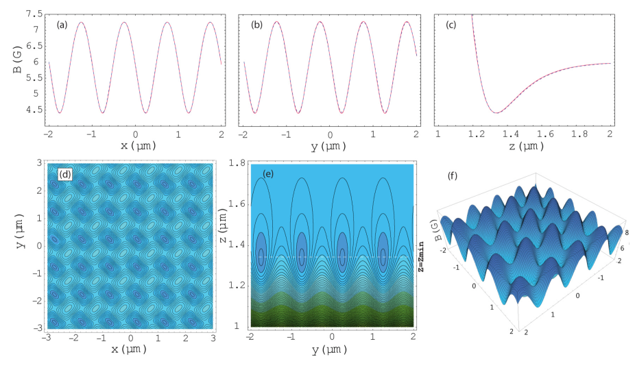
For =10 sublayers, great versatility can be seen in Fig.5 (a), (b) and (c) between analytical and numerical plots of magnetic field along the -, - and -directions, close to the center of the permanent magnetic lattice. By adding more sublayers, we expect to have a sawtooth structure with better accuracy. Numerical and analytical results for the 2D magnetic lattice have been compared in tables 2 and 3 for = 10 and 20, respectively. For example, symmetrical magnetic traps in - and - directions for =10 can be obtained at =1.33m from bottom of the layers by applying the bias field = 5.6G and = 2.18G. The minimum of the magnetic field at the center of each microtrap is 4.41G.
| Parameters (k) | Definition | =10 | =20 |
|---|---|---|---|
| / | Minimum Potential | 296 | 287 |
| / | Potential barrier height | 201 | 213 |
| in -direction | |||
| / | Potential barrier height | 201 | 213 |
| in -direction | |||
| / | Potential barrier height | 107 | 119 |
| in -direction | |||
| / | Energy level spacing in | 10 | 10 |
| -direction | |||
| / | Energy level spacing in | 10 | 10 |
| -direction | |||
| / | Energy level spacing in | 15 | 15 |
| -direction |
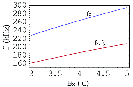
According to Fig.6, a bias magnetic field along the x-direction can change the trap frequencies.
It is also possible to create permanent magnetic lattices with different barrier heights in the - and - directions. For example, if we apply a bias magnetic field with = 10G and =0.87G the trap depths along the - and -directions 4.5G and 15G, respectively. For this bias field, corresponding frequencies along the - and -directions are not the same and atoms feel two different barrier heights in the - and -directions, respectively. Decreasing or increasing potential barrier heights will change the rate of tunneling between lattice sites. Different rates is useful in quantum tunnelling experiments.
4 Conclusion
We have introduced a new permanent magnetic lattice based on perpendicularly magnetized thin sawtooth films. This lattice can produce Ioffe-Pritchard 2D and 3D microtraps in 1D and 2D lattices, respectively for holding ultracold atoms and BECs when a bias field is applied. We have presented analytical expressions for parameters such as location of the microtraps, curvatures of the magnetic field and also frequencies and trap depth close to the center of the lattice. We also have shown that numerical calculations are in agreement with analytical ones for two different number of the sublayers n. The components of homogenous external magnetic field along - and -directions, and , can change the trap depth and frequencies of microtraps. Control over the trap depths let us to handle tunneling parameters via increasing or decreasing potential barrier heights for cold atoms and BECs which has wide applications in quantum information processing and superfluid to Mott insulator quantum phase transition studies. Trap density is 106 atoms/mm2 for loading cold atoms and BECs. Considering the current technology, it should be easy to manufacture the proposed nano-structure.
Acknowledgements.
Amir Mohamadi would like to thank Farhood Ahani and Aref Pariz for helpful discussions.References
- (1) H. J. Metcalf and P. Straten, Laser Cooling and Trapping, (Springer, USA, 2002).
- (2) W. D. Phillips, Rev. Mod. Phys. 70, 721-741 (1998).
- (3) M. D. Barrett, J. A. Sauer, and M. S. Chapman, Phys. Rev. Lett. 87, 010404 (2001).
- (4) T. Takekoshi, B. M. Patterson, and R. J. Knize, Phys. Rev. Lett. 81, 5105-5108 (1998).
- (5) T. W. H. ansch and A. L. Schawlow, Opt. Comm. 13, 68-69 (1975).
- (6) J. Mozley et al, Eur. Phys. J. D 35, 43 57 (2005).
- (7) D. Jaksch, C. Bruder, J. I. Cirac, C. W. Gardiner, and P. Zoller, Phys. Rev. Lett. 81, 3108-3111 (1998).
- (8) Y. H. Chen, W. Wu, H. S. Tao, and W. M. Liu, arXiv:1005.0428v2.
- (9) C. J. Pethick and H. Smith,Bose-Einstein condensation in dilute gases,(Cambridge University Press, Cambridge, England, 2008).
- (10) M. Guglielmino, V. Penna, and B. Capogrosso-Sansone, Phys. Rev. A. 82, 021601(R) (2010).
- (11) M. Greiner, O. Mandel, T. Esslinger, T. Hansch, and I. Bloch , Nature, 415, 39 (2002).
- (12) J. B. Trebbia, J. Esteve, C. I. Westbrook, and I. Bouchoule, Phys. Rev. Lett. 97, 250403 (2006).
- (13) H. van Amerongen, J. J. P. van Es, P. Wicke, K.V. Kheruntsyan, and N. J. van Druten, Phys. Rev. Lett. 100, 090402 (2008).
- (14) T. J. Alexander, M. Salerno, E. A. Ostrovskaya, and Yuri S. Kivshar, Phys. Rev. A. 77, 043607 (2008).
- (15) M. Nakahara and T. Ohmi, Quantum computing From Linear Algebra to Physical Realizations, (CRC Press, USA, 2008).
- (16) G. Birkl and J. Fort agh, Laser and Photon. Rev. 1, 12-23 (2007).
- (17) E. A. Hinds, M. G. Boshier, and I. G. Hughes, Phys. Rev. Lett. 80, 645-649 (1998).
- (18) S. Ghanbari, T. D. Kieu, A. Sidorov, and Peter Hannaford, J. Phys. B. 39, 847-860 (2006).
- (19) S. Ghanbari, T. D. Kieu, and Peter Hannaford, J. Phys. B: At. Mol. Opt. Phys. 40, 1283 (2007).
- (20) D. Muller, D. Z. Anderson, R. J. Grow, P. D. D. Schwindt, and E. A. Cornell , Phys. Rev. Lett. 83, 1283-1294 (1999).
- (21) J. Reichel, W. H nsel, and T. W. H nsch, Phys. Rev. Lett. 83, 3398-3401 (1999).
- (22) C.D.J. Sinclair et al., Eur. Phys. J. D 35, 105 110 (2005).
- (23) J. Fortgh and C. Zimmermann, Rev. Mod. Phys. 79, 235 (2007).
- (24) S. Du and E. Oh, hys. Rev. A. 79, 013407 (2009).
- (25) A. Mohammadi, S.Ghanbari, and A.Pariz, arXiv:1007.2912v1 (2010).
- (26) T. Fernholz, R. Gerritsma, S. Whitlock, I. Barb, and R. J. C. Spreeuw, Phys. Rev. A. 77, 033409 (2008).
- (27) R. Gerritsma et al., Phys. Rev. A. 76, 033408 (2007).
- (28) M. Singh, R. McLean, A. Sidorov, and P. Hannaford, Phys. Rev. A. 79, 053407 (2009).
- (29) A.I. Sidorov et al., Acta Phys. Pol. B. 33 2137 (2002).
- (30) Available from: http://www.esrf.eu/Accelerators/Groups/ InsertionDevices/Software/Radia/Documentation/Introduction