Resonant Photovoltaic Effect in Surface State Electrons on Liquid Helium
Abstract
We observed an ultra-strong photovoltaic effect induced by resonant intersubband absorption of microwaves in a two-dimensional electrons system on the surface of liquid helium. The effect emerges in the regime of microwave-induced vanishing of dissipative conductance, , reported previously [D. Konstantinov and K. Kono: Phys. Rev. Lett. 105 (2010) 226801)] and is characterized by a nonequilibrium spatial distribution of electrons in the confining electrostatic potential. The electrostatic energy acquired by an electron exceeds other relevant energies by several orders of magnitude.
pacs:
73.20.At, 73.21.-b, 72.20.My, 78.70.GqA nondegenerate two-dimensional electron system can be formed on the surface of liquid helium Andrei ; Monarkha_book . Here, surface state subbands with energies appear owing to the attractive image force, the repulsive surface barrier, and an electric field applied perpendicular to the surface. Below 1 K, almost all electrons are frozen into the lowest subband forming an equipotential 2D charge layer confined on helium surface. It is a strongly-correlated system of particles interacting via unscreened Coulomb interaction. A recent work reported an effect of vanishing conductance in this system under resonant excitation by microwaves Konstantinov2010 . In the experiment, the inter-subband transition is excited using radiation with angular frequency such that . Under such conditions, the longitudinal conductivity , measured as a time-averaged response using a Corbino disc, oscillates upon varying the perpendicular magnetic field , showing a sequence of minima shifted to lower values with respect to satisfying the relation , where is the cyclotron frequency and (the lowest was limited by T employed in the experiment). At low , the conductivity drops abruptly to zero. In accordance with the standard tensor relation, the vanishing conductivity at the minima corresponds to vanishing resistivity suggesting connection with radiation-induced zero-resistance states (ZRS) of degenerate 2D electron gas in high mobility GaAs/AlGaAs heterostructures Mani2002 ; Zudov2003 .
In this work, we study a transient response of the electron system upon irradiation in the regime of vanishing conductance. We show that the radiation causes strongly nonequilibrium distribution of electrons in the confining electrostatic potential produced by the surrounding metallic electrodes. This corresponds to an increase of the electrostatic potential energy of an electron of the order electron volt, which exceeds any relevant energies, such as for example the average kinetic energy of the electrons, by orders of magnitude. The effect must have strong connection with the zero-resistance states.
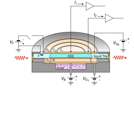
Figure 1 shows a schematic diagram of the experimental apparatus. Liquid 3He is condensed into a cell having flat cylindrical shape, which contains a sintered silver heat exchanger to ensure sufficient heat contact between the liquid and the cell body. The liquid level is set midway between two parallel plates, each having a radius of 13 mm, separated by mm. The bottom plate is divided into electrodes B and G1 by a gap at a distance of 10 mm from the center of the plate, while the top plate is divided into electrodes C1, C2 and G2 by two gaps at distances of 7 and 10 mm from the center. Each of the three gaps has a width of 0.2 mm. Electrodes C1 and C2 form a Corbino disk (dc-grounded), from which can be determined as described previously Konstantinov2010 . Electrons are produced by briefly heating a tungsten filament F, while a positive bias is applied to the electrode B and all other electrodes are grounded. The nearly uniform areal density of electrons, which form a circular pool on the surface beneath the electrode, is determined by the condition of complete screening of electric field above the charged surface of liquid Konstantinov2010 . A typical bias of V used in this experiment corresponds to the areal density of electrons cm-2. However, this number can vary due to accidental discharge of electrons or change of the electrical biases applied to surrounding electrodes. A careful calibration procedure, that allows for the total number of electrons on the surface to be determined, is described further in the text.
The positively biased electrodes provide a neutralizing background, which counteracts the Coulomb repulsion between electrons and prevents them to spread away. Within a conducting charged layer, the in-plane electric field is almost zero. Below 1 K, the average thermal kinetic energy of an electron does not exceed eV. Therefore, a built-in electric field, which compensates the diffusion current of electrons in a density gradient, can be neglected, and the equilibrium spatial distribution of 2D electrons can be obtained numerically assuming constant electrical potential across the entire charged layer Wilen1988 . The equilibrium density profiles for different electrode biases will be discussed later.
Electrons are tuned for the intersubband resonance with the applied microwaves by adjusting the electrode bias , which changes the electric field and shifts the subband energies because of the Stark effect. For microwaves of frequency GHz employed in this experiment, the resonance is centered at V. Usually, the guard electrodes G1 and G2 are kept at zero potential. Previously, the photo-induced change in was observed upon cw irradiation and measuring a time-averaged response of the electrons to a driving in-plane electric field Konstantinov2010 . The present work aims at detecting the transient photoresponse of surface electrons in the absence of such a field. For this purpose, the incident microwave power is pulse modulated using a low-frequency (0.5-6 Hz) square waveform, and the current signals and induced in electrodes C1 and C2, respectively, are recorded using a digital storage oscilloscope following the current preamplifiers (100 Hz bandwidth). Alternatively, these currents or their difference are measured by a lock-in amplifier using the microwave modulating signal as a reference.
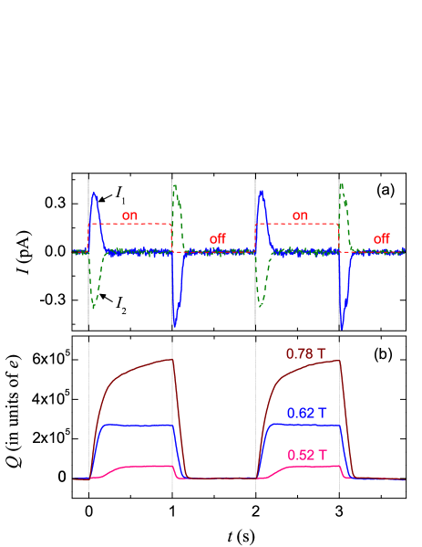
Figure 2(a) shows an example of the transient current signals and obtained at K and T. The value of corresponds to the conductance minimum. In order to improve signal-to-noise ratio, the traces shown in the figure were obtained by averaging over about 500 sweeps. For reference, the modulation of the microwave power by the square waveform is shown in Fig. 2(a) by a dashed line. First of all, note that the current signals and are comparable in magnitude and have opposite signs. From this result, we obtain the following qualitative picture. Upon switching the power on, the electrons are pulled towards the edge of the electron pool, causing the depletion (accumulation) of the charge in the central (peripheral) region of the pool. Correspondingly, the positive (negative) current is induced in electrode C1 (C2) by the flow of the image charge. The surface charge flows until a new spatial distribution of 2D electrons in the unchanged confining electrostatic potential is established, after which the currents and becomes zero. Correspondingly, the displacement of electrons with respect to the neutralizing background induces variation in the electrostatic potential energy of an electron, and therefore a non-zero build-in electric field, to develop in the charged layer. Upon switching the power off, the displaced surface charge flows back to restore the equilibrium distribution of electrons. Correspondingly, a negative (positive) current of the image charge is induced in C1 (C2).
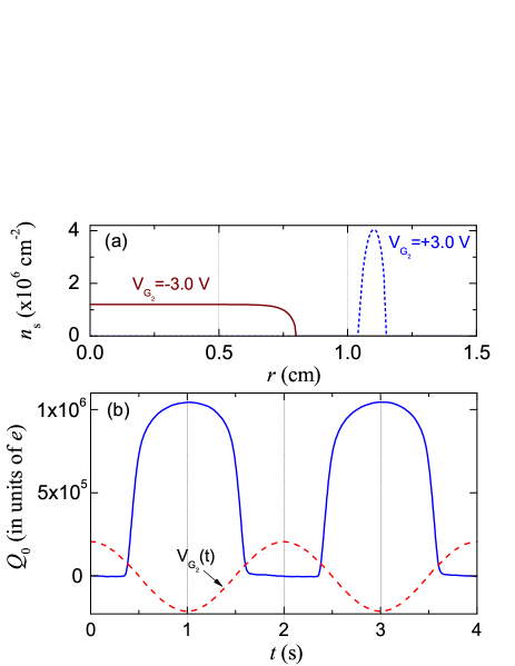
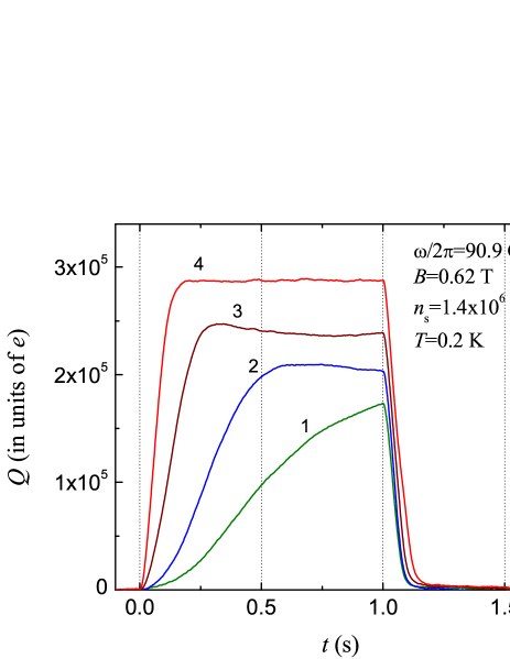
Next, we estimate the amount of the charge displaced under irradiation. The cumulative charge flowing from, for example, the electrode C2 is obtained by integrating the measured current . (in units of the elementary charge ) is shown in Fig. 2(b) for three values of corresponding to the conductance minima , 5, and 6. To make comparison of this quantity with the total image charge induced on electrode C1 in the dark, the latter was experimentally determined from the following procedure. At V, we apply an ac (0.5 Hz) potential of the amplitude 3.0 V to the electrode G2. When V, the surface charge is pulled out from the center to form a ring beneath the electrode G1, as confirmed numerically by calculating the charge profile as shown in Fig. 3(a). As decreases to -3.0 V, the charge is pushed back into the region beneath the electrode C1 (see Fig. 3(a)) inducing the negative current through the electrode C1. This current is measured and integrated to obtain the positive charge in the electrode C1 induced by the surface electrons. The induced charge is shown in Fig. 3(b). We find that a total image charge of about is induced on the electrode C1. The comparison of this value with in Fig. 2(b) shows that a very large fraction (more than 50) of the surface charge can be displaced upon irradiation. From this procedure and the numerial calculations we find the total number of electrons and the areal density of electrons cm-2 in the dark at V and .
The displacement of negative charged electrons induces a nonzero in-plane electric field to develop across the system. It is straightforward to estimate the radially symmetric built-up difference of electrical potential across the charge layer. For the geometry shown in Fig. 1, the electrical potential of the charge layer is given by , where is the distance between top and bottom plates and we neglect small deviation of the dielectric constant of liquid helium from unity. Thus, the displacement of 50 of electrons corresponds to the potential difference between the central and peripheral parts . For the areal density estimated above this gives V. This result is confirmed by the numerical calculations and corresponds to the increase in electrical potential energy of a single electron exceeding other relevant energy scales such as, for example, the intersubband energy difference or average thermal kinetic energy of an electron, by several orders of magnitude.
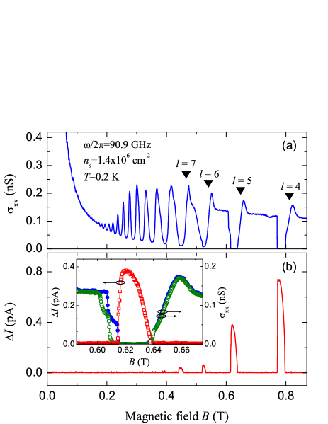
Figure 4 shows a comparison between measured under cw irradiation and recorded under 100 modulation of the incident microwave power. Both sets of data are obtained upon increasing the magnetic field at K and at the same level of microwave power. A nonzero signal is observed only in the intervals of near the conductance minima corresponding to , 5, 6, and 7. As described above, this signal is due to the currents induced in electrodes C1 and C2 by the displacement of the surface charge. No signal is observed when electrons are tuned away from the intersubband resonance by changing the electrical bias . Simultaneously, the detuning results in the complete disappearance of the magnetooscillations and zero-conductance states Konstantinov2010 . Importantly, the disappearance of in the electron system tuned away from the resonance, as well as when the surface is completely discharged by reversing the sign of , confirms that the current is not produced in the conducting electrodes by, for example, microwave-induced heating, vibrations, or other effects.
The inset of Fig. 4(b) shows the signal in a narrow range of near the conductance minimum. The signal emerges abruptly upon slowly increasing . This feature is consistent with the abrupt drop of to zero recorded upon the upward sweep of (solid circles). The abrupt change of and is an indication of instability of the electron system in ZRS regime due to, for example, the resonant overheating of electrons by microwave radiation Konstantinov2009 . Upon the downward sweep of , (open circles) exhibits hysteresis. Such hysteresis is a feature of a metastable state coexisting with the global stable state of electron system. The coexistence regime can be observed only upon continuous irradiation by microwaves. When the power is repeatedly switched on and off, the system remains in the global stable state corresponding to equilibrium spatial distribution of charge. Accordingly, the variation of in Fig. 4(b) does not show dependence on the direction of sweeping.
The kinetics of the radiation-induced displacement of surface charge strongly depends on different parameters such as the microwave power, the density of electrons, and the index . The cumulative charge measured for cm-2, T, and at four different power levels is shown in Figure 5. For the fully screened electron system in our experiment, the typical time required to recover the equilibrium spatial distribution, the relaxation time , can be estimated as , where is the capacitance between the charged layer and the surrounding electrodes. For pF and S, this gives s, which is in agreement with the fall time of upon switching the microwaves off, as shown in Fig. 4. In contrast, the time required to establish the redistribution of electrons across the layer upon switching the power on, as can be seen from the rising edge of , can exceed 1 s at sufficiently low powers. Even at high powers, the build-up of charge is slowed by either increasing or choosing the conductance minima of a high index . Remarkably, a time delay of up to 0.1 s between the application of microwaves and the onset of the charge motion can be observed, as shown, for example, by the data labeled as 0.52 T in Fig. 2(b). This slow redistribution kinetics is in extreme contras with a much faster rate of microwave-induced inter-subband transitions on the order - s-1.
Finally, we discuss the possible explanations for the observed photovoltaic effect. Radiation can exert an optical force on a charged particle, as is used for the cooling and trapping of atoms and ions Metcalf_book . This force can be estimated as the expectation value , where describes the interaction of the particle with the radiation field and is the distance along the surface. Our estimations show that the optical force is too weak to directly account for the displacement of charge reported here. The appearance of this effect at the minima of the conductance oscillations indicates the inherent relationship between the redistribution of charge and . In addition, an important question is the relation of the effect reported here to photovoltaic effects, which accompany the microwave-induced resistance oscillations in GaAs/AlGaAs heterostructures Bykov2008 ; Willett2004 ; Dorozhkin2009 ; Bykov2010 . In heterostructures, the observed oscillations of photocurrent and photovoltage were interpreted in terms of built-in electric fields due to band bending at contacts Dorozhkin2009 ; Dmitriev2009 . Clearly, we do not have such fields in our system where the surface charge layer is maintained at a constant electrical potential at least without irradiation by microwaves. The microwave field gradient in the near-contact region can generate a ponderomotive force acting on 2D electrons in heterostructures, which may be a possible explanation for the ZRS in this system Mikhailov2011 . Such an effect is unlikely to occur in our system because the electrons are not in contact with the conducting electrodes. Recently, it was proposed that microwave-induced oscillations of in surface state electrons on liquid helium originate from the intersubband scattering of electrons under the condition of nonequilibrium filling of the excited subband Monarkha2011 ; Monarkha2012 . This mechanism can result in an absolute negative , causing current instability and the formation of a steady azimuthal current , such that Andreev2003 . In a perpendicular magnetic field, the steady configuration would require a radial Hall field, , where . The only way to produce such a field is to displace electrons radially. The measured of the order 1 V/cm would correspond to the current density 1nA/cm. This value must be compared with predictions of nonlinear transport theory which is not available at present. Finally, the microwave stabilization of edge trajectories, which was proposed recently to explain ZRS in heterostructures, naturally gives the correct direction of the charge displacement Chepelianskii2009 . The creation of ballistic channels at the sample edges due to microwave irradiation combined with a pumping mechanism through the inter-subband excitation might lead to an accumulation of charge at the edges. This possibility, as well as other outlined scenarios, require thorough theoretical investigation.
In summary, we studied the photoresponse of a circular pool of electrons on the surface of liquid helium subjected to a perpendicular magnetic field. We found out that under the resonant intersubband-absorption of microwaves, a large fraction of electrons is displaced from the center of the pool towards the edge producing a strongly nonequilibrium distribution of charge. The effect emerges at minima of the microwave-induced magneto-oscillations and suggests close connection with the states of vanishing resistance.
We thank H. Bouchiat and D.L. Shepelyansky for helpful discussions. This work was supported in part by Grant-in-Aids for Scientific Research from MEXT. D.K. acknowledges an Incentive Research Grant from RIKEN and internal grant from the Okinawa Institute of Science and Technology.
References
- (1) Electrons on Helium and Other Cryogenic Substrates, edited by E.Y. Andrei (Kluwer Academic, Dordrecht, 1997).
- (2) Y. Monarkha and K. Kono: Two-Dimensional Coulomb Liquids and Solids (Springer, Berlin, 2004).
- (3) D. Konstantinov and K. Kono: Phys. Rev. Lett. 105 (2010) 226801.
- (4) R. G. Mani, J.H. Smet, K. von Klitzing, V. Narayanamurti, W. B. Johnson, and V. Umansky: Nature (London) 420 (2002) 646.
- (5) M. A. Zudov, R. R. Du, L. N. Pfeiffer, and K. W. West: Phys. Rev. Lett. 90 (2003) 046807.
- (6) L. Wilen and R. Giannetta: J. Low Temp. Phys. 72 (1988) 353.
- (7) D. Konstantinov, M. I. Dykman, M. J. Lea, Yu. P. Monarkha, and K. Kono: Phys. Rev. Lett. 103 (2009) 096801.
- (8) H. J. Metcalf and P. van der Straten: Laser Cooling and Trapping (Springer, New York, 1999).
- (9) R. L. Willett, L. N. Pfeiffer: and K. W. West, Phys. Rev. Lett. 93 (2004) 026804.
- (10) A. A. Bykov: JETP Lett. 87 (2008) 233.
- (11) S. I. Dorozhkin, I. V. Pechenezhskiy, L. N. Pfeiffer, K. W. West, V. Umansky, K. von Klitzing, and J. H. Smet: Phys. Rev. Lett. 102 (2009) 036602.
- (12) A. A. Bykov: JETP Lett. 91 (2010) 361.
- (13) I. A. Dmitriev, S. I. Dorozhkin, and A. D. Mirlin: Phys. Rev. B 80 (2009) 125418.
- (14) S. A. Mikhailov: Phys. Rev. B 83 (2011) 155303.
- (15) Yu. P. Monarkha: Fiz. Nizk. Temp. 37 (2011) 108.
- (16) Yu. P. Monarkha: Fiz. Nizk. Temp. 38 (2012) 579.
- (17) A. V. Andreev, I. L. Aleiner, and A. J. Millis: Phys. Rev. Lett. 91 (2003) 056803.
- (18) A. D. Chepelianskii and D. L. Shepelyansky: Phys. Rev. B 80 (2009) 241308(R).