Spin-thermo-electronic oscillator based on inverse giant magnetoresistance
Abstract
A spin-thermo-electronic valve with the free layer of exchange-spring type and inverse magnetoresistance is investigated. The structure has S-shaped current-voltage characteristics and can exhibit spontaneous oscillations when integrated with a conventional capacitor within a resonator circuit. The frequency of the oscillations can be controlled from essentially dc to the GHz range by the circuit capacitance.
I Introduction
Electrons in ferromagnetic conductors are differentiated with respect to their spin due to the exchange interaction which leads to a splitting of the corresponding energy bands and to a non-vanishing polarization of the conduction electrons. This spin polarization gives rise to a number of ”spintronic” effects in magnetic nanostructures, such as Giant Magnetoresistance (GMR) Baibich ; Binasch and Spin-Transfer-Torque Slonczewski ; Berger .
A conventional GMR spin-valve has low resistance in the parallel configuration of the two ferromagnetic layers and high resistance in the antiparallel configuration. The GMR is said to be inverse when the low resistance state corresponds to the antiparallel orientation of the ferromagnets Vouille . Inverse GMR is observed in, for example, spin-valves incorporating minority carrier ferromagnetic layers George ; Renard ; Hsu ; Voulle2 . Another possible implementation of the inverse GMR spin-valve, demonstrated in this paper, relies on an antiparallel exchange-pinning of two ferromagnetic layers of different coercivity to two antiferromagnetic layers.
We have previously analyzed a novel spin-thermo-electronic (STE) oscillator JAP based on a GMR exchange-spring multilayer Davies having a N-shaped current-voltage characteristic (IVC), connected in series to an inductor (L) which performs the function of current limiting in the circuit and thereby determines its resonance frequency. A tunable inductor, such as the one having a magnetic core Vlad1 ; Vlad2 , can be used to achieve a tunable resonator. However, in applications where the device footprint is tightly budgeted, it may be advantageous to employ a mirror-circuit configuration. Namely, an inverse GMR spin-valve with an S-shaped IVC connected to a capacitor (C) in parallel. This paper provides a detailed analysis of this new structure as well as a comparison of the two STE oscillator designs. We show that the STE-C design proposed herein offers an attractive, compact alternative to the STE-L oscillator discussed previously JAP .
II S-shaped current-voltage characteristic under Joule heating: control of the magnetization direction by dc bias current
We consider a system of three ferromagnetic layers in which two strongly ferromagnetic layers 0 and 2 are exchange coupled through a weakly ferromagnetic spacer (layer 1) while layer 3 is nonmagnetic as illustrated in Fig.1. We assume that the Curie temperature of layer 1 is lower than the Curie temperatures of layers 0, 2; we also assume the magnetization direction of layer 0 to be fixed; layer 2 is subject to a magnetic field directed opposite to the magnetization of layer 0, which can be an external field, the fringing field from layer 0, or a combination of the two. We require this magneto-static field to be weak enough so that at low temperatures the magnetization of layer 2 is kept parallel to the magnetization of layer 0 due to the exchange interaction between them via layer 1. In the absence of the external field and if the temperature is above the Curie point of the spacer, , this tri-layer is similar to the spin-flop ‘free layer’ widely used in memory device applicationsWorledge .
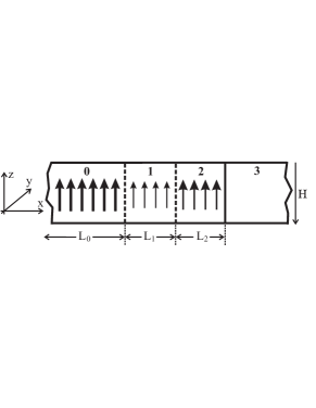
As it was shown in paper JAP parallel orientations of the magnetization in layers 0, 1 and 2 becomes unstable if the temperature exceeds some critical temperature . The magnetization direction in layer 2 tilts with an increase of the stack temperature in the temperature range . The dependence of the equilibrium tilt angle between the magnetization directions of layers 0 and 2 on and the magnetic filed is determined by the equation JAP
| (1) |
where
| (2) |
Here and are the widths and the magnetic moments of layers 1 and 2, respectively; is the exchange constant, is the exchange energy in layer 1 and is the lattice spacing. The parameter is the ratio between the magnetic energy and the energy of the stack volume for the inhomogeneous distribution of the magnetization. At low temperatures the exchange energy prevails, the parameter and Eq. (II) has only one root, , thus a parallel orientation of magnetic moments in layers 0, 1 and 2 of the stack is thermodynamically stable. However, at temperature , for which
two new solutions appear. The parallel magnetization corresponding to is now unstable, and the direction of the magnetization in region 2 tilts with an increase of temperature inside the interval . According to Eq.(2) the critical temperature of this orientational phase transition Giovanni is equal to
| (3) |
If the stack is Joule heated by current its temperature is determined by the heat-balance condition
| (4) |
and Eq. (II), which determines the temperature dependence of . Here is the voltage drop across the stack, is the heat flux from the stack and is the total stack magnetoresistance.
The differential conductance of the stack JAP is
| (6) |
where means the derivative of the bracketed quantity with respect to , and
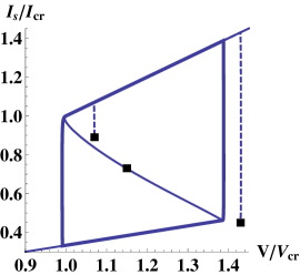
As follows from Eq.(6) the current-voltage characteristic may be N- or S-shaped depending on whether the magnetoresistance of the stack is normal or inverse. In the case that the stack has a normal magnetoresistnace (that is ) the IVC is N-shaped so nonlinear current and magnetization-direction oscillations may spontaneously arise if the stack is incorporated in a voltage biased electrical circuit in series with an inductor JAP . In this paper we consider the situation in which the stack has an inverse GMR inverse , i.e. . As one can see from Eq.(6), if , the numerator of the differential conductance is always positive while the denominator can be negative and hence the IVC of the stack is S-shaped as illustrated in Fig. 2.
For the magnetoresistance of the stack in the form
| (7) |
where
| (8) |
one finds that that the differential conductance if
| (9) |

In Section III we show that in the case of the S-shaped IVC current and magnetization oscillations arise if the stack is incorporated in a current biased circuit in parallel with a capacitor (see Fig.4). In this case the thermo-electonic control of the relative orientation of layers 0 and 2 may be of two types depending on the ratio between the resistance of the stack and the resistance of the rest of the circuit .
As one can see from Fig.2, if the bias current through the stack is controllably applied (that is ), the voltage drop across the stack is uniquely determined from the IVC and hence the relative orientation of the magnetization of layers 0 and 2 (that is the tilt angle ) can be changed smoothly from parallel () to anti-parallel by varying the bias current through the interval . This corresponds to moving along the branch of the IVC. The dependence of the magnetization direction on the current flowing through the stack is shown in Fig. 3.

In the voltage-bias regime, on the other hand, where the resistance of the stack is much larger than the resistance of the rest of the circuit, , the voltage across the stack is kept at a given value approximately equal to the bias voltage. Since the IVC is S-shaped, the stack can now be in a bistable state: in the voltage range between points and there are three possible values of the current for one fixed value of voltage (see Fig. 2). The states of the stack with the lowest and the highest currents are stable, while the state of the stack with the middle value of the current is unstable. Therefore, a change of the voltage results in a hysteresis loop: an increase of the voltage along the branch of the IVC leaves the magnetization directions in the stack parallel () up to point , where the current jumps to the upper branch , the jump being accompanied by a fast switching of the stack magnetization from the parallel () to the antiparallel orientation (). A decrease of the voltage along the IVC branch keeps the stack magnetization antiparallel up to point , where the current jumps to the lower branch of the IVC and the magnetization of the stack returns to the parallel orientation ().
In the next section we show that if the stack is connected in parallel with a capacitor, and the capacitance exceeds some critical value, the above time independent state becomes unstable and spontaneous temporal oscillations appear in the values of the current, voltage across the stack, temperature, and direction of the magnetization.
III Self-excited electrical, thermal and directional magnetic oscillations.
We consider now a situation where the magnetic stack under investigation is incorporated into an electrical circuit in parallel with a capacitor of capacitance and the circuit is biased by a DC current , illustrated by the equivalent circuit of Fig. 4. The thermal and electrical processes in this system are governed by the set of equations
| (10) |
where is the heat capacity. The relaxation of the magnetic moment to its thermodynamic equilibrium direction is assumed to be the fastest process in the problem, which implies that the magnetization direction corresponds to the equilibrium state of the stack at the given temperature . In other words, the tilt angle adiabatically follows the time-evolution of the temperature and hence its temperature dependence is given by Eq. (II).
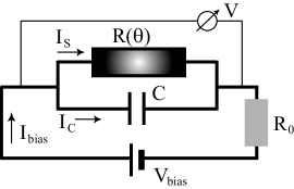
A time dependent variation of the temperature is accompanied by a variation of the tilt angle and hence by a change in the voltage via the dependence of the magneto-resistance on this angle, .
The system of equations Eq.(10) has one time-independent solution () which is determined by the equations
| (11) |
This solution is identical to the solution of Eqs.(II,4) that determines the S-shaped IVC shown in Fig.2 with a change and .
In order to investigate the stability of this time-independent solution we write the temperature, current and angle as a sum of two terms,
| (12) |
where , and are small corrections. Inserting Eq.(12) into Eq.(10) and Eq. (II) one easily finds that the time-independent solution Eq.(11) is always stable at any value of the capacitance if the bias current corresponds to a branch of the IVC with a positive differential resistance (branches a-a’ and 0-b in Fig.2). If the bias current corresponds to the branch with a negative differential resistance (, see Fig.2), the solution of the set of linearized equations is , and where , and are any initial values close to the time-independent state of the system, and
| (13) |
where
| (14) |
is the differential resistance, .
As one can see from Eq.(13), the time-independent state Eq.(11) looses its stability if the capacitance exceeds the critical value , that is . In this case a limit cycle appears in plane () (see, e.g., Ref. Andronov ), associated with the arising self-excited, non-linear, periodic oscillations in temperature, , and voltage, . These are accompanied by oscillations of the current through the stack, , and of the magnetization direction . In the case when , the system undergoes nearly harmonic oscillations around the steady state (see Eq.(12)) with frequency . Therefore, the temperature, , the voltage drop across the stack, , the current through the stack, , and the magnetization direction, , perform a periodic motion with frequency
| (15) |
With a further increase of the capacitance the size of the limit cycle grows, the amplitude of the oscillations increases and the oscillations become anharmonic, with their period decreasing with increasing capacitance.
In order to investigate the time evolution of the voltage drop and the current through the stack in more detail it is convenient to change variables to and introduce auxiliary current and voltage related to each other through Eqs. (4) and (II). Thus, we define
| (16) |
where . Comparing these expressions with Eq. (4) shows that at any moment Eq. (16) gives the stationary IVC of the stack, , which is an inverse function of the current-voltage characteristic defined by Eq. (5) and shown in Fig. (2).
Differentiating with respect to and using Eqs. (10) and (16) one finds that the dynamic evolution of the system is governed by
| (17) |
where
Eq. (16) indicates that at any moment the current through the stack is coupled with the auxiliary voltage by the following relation:

The coupled equations (17) have only one time-independent solution where is the voltage-current characteristic (its inverse function is shown in Fig.2). However, in the interval this solution is unstable with respect to small perturbations if . As a result periodic oscillations of and appear spontaneously, with , moving along a limit cycle. The limit cycle in the - plane is shown in Fig. 5.
Eq.(II) and Eq.(16) show that the magnetization direction, , and the stack temperature follow these electrical oscillations adiabatically according to the relation
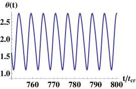
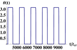
Temporal oscillations of are shown in Fig. 6.
According to Eq.(17) the ratio between the characteristic evolution times of the voltage and current increases with an increase of the capacitance, resulting in a qualitative change of the character of oscillations in the limit . In this case the current and the voltage slowly move along branches and of the IVC (see Fig.2)) at the rate (here ), quickly switching between these branches at points and with at the rate of (see Fig. 7). Therefore, the stack in this limit periodically switches between the parallel and antiparallel magnetic states, as shown in Fig. 8.
Using equations Eq.(11) one can estimate the order of magnitude of the critical capacitance , Eq.(14), and the oscillation frequency , Eq.(15), as and , where is the heat capacity per unit volume, is the resistivity, and is the characteristic size of the stack. For point contact devices with typical values of , K, cm, and assuming that cooling of the device can provide the sample temperature one finds for the characteristic values of the critical capacitance and the oscillation frequency and , respectively.
We will now show how the material system discussed above, with inverse GMR, can be fabricated using differential exchange-biasing. A schematic of the layer structure is shown in Fig. 9 (a). The two ferromagnetic layers of the spin-valve (FM 1 and FM 2), each exchange pinned by an antiferromagnet (AFM 1 and AFM 2), are separated by a non-magnetic metal spacer (NM). Normally, the exchange-biasing procedure performed at a high field results in the two ferromagnets being pinned with their magnetization parallel to each other. In order to demonstrate inverse magnetoresistance the exchange pinning must be altered such that the magnetization of the two ferromagnets become antiparallel. This can be done in two ways.
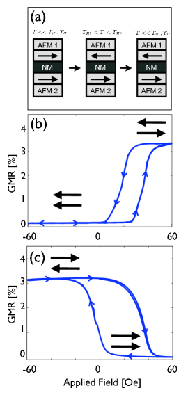
First; the blocking temperature of the two antiferromagnetic layers can be designed in fabrication such that one is lower than the other, or ref:ThermalMRAM . By heating the sample to a temperature above the lower blocking temperature () but below the higher blocking temperature (), the magnetization of FM 1 (FM 2) can be rotated by applying an external field. With FM 1 and FM 2 now antiparallel the sample is cooled down to room temperature and the two ferromagnetic layers are pinned in opposition.
Second; by using ferromagnets with different coercivity, , and heating the sample to a temperature above both and . At this temperature the ferromagnet with lower coercivity, FM 1 (FM 2), can be rotated in an external field if (), where is the applied field. With FM 1 and FM 2 now antiparallel the sample is cooled down to room temperature. A schematic of these two methods are shown in Fig. 9 (a). Below, we demonstrate the second method for obtaining an inverse GMR spin-valve using a practical material stack.
A series of films were deposited on thermally oxidized Si substrates using magnetron sputtering at a base pressure better than Torr. 15 nanometer thick IrMn is used for AFM 1 and AFM 2. FM 1 is a thin bilayer of CoFe/NiFe and FM 2 is made up of CoFe/NiCu/CoFe/NiFe/CoFe, such that the two layers have different coercivity (). To induce exchange coupling at the AFM/FM interfaces the deposition was carried out in a magnetic field higher than 350 Oe. The complete structure of the sample was NiFe 3/ IrMn 15/ CoFe 2/ NiCu 30/ CoFe 2/ NiFe 6/ CoFe 4/ Cu 7/ CoFe 5/ NiFe 3/ IrMn 15/ Ta 5, with the thicknesses in nanometers.
Using a vibrating sample magnetometer (VSM) equipped with an oven, the magnetization and switching fields of FM 1 and FM 2 could be monitored while the temperature was increased. At 180∘C the temperature was higher than both and which made it possible to align FM 1 and FM 2 antiparallel (since ). The external magnetic field was then removed and the sample was cooled down to room temperature. The minor magnetoresistance loop (current in plane magnetoresistance versus applied field when only the magnetization of FM 2 is switched) before and after the above field-heat treatment is shown in Fig. 9 (b). It can be seen that before the heat treatment the resistance increases when a positive field of 30 Oe is applied. The same measurement for the same sample but after the heat treatment is shown in Fig. 9 (c). The magnetoresistance has now become inverse which means that the resistance decreases when a positive field is applied. The coercivity of FM 2 chosen for this demonstration of differential exchange pinning has increased somewhat as a result of the field-heat treatment. This issue should yield to optimization of the material stack and working with smaller blocking temperatures.
As regards to the size of the integrated oscillator, let us assume the typical resistance of the STE-valve to be 50 Ohm and the operating frequency GHz, and estimate the required inductance and capacitance of the circuit. Thus, Ohm yields H while Ohm yields F. The typical inductance of an on-chip inductor is 1 nH per mm of the wire length, somewhat enhanced if the wire is turned in to a spiral. Therefore the required chip area would be millimeters squared in size. A square parallel plate capacitor, estimated using the standard formula, for a typical dielectric material of a few nm thick insulator would measure 10 micrometers on the side. Obviously, a 10,000-fold reduction in the typical footprint should be achievable in principle by employing a device based on an S-shaped STE-valve. In systems where tunability and high power are desirable, the N-shaped inductor based design may be preferable.
IV Conclusion
We have shown that Joule heating of an exchange-spring nanopillar with an inverse magneto-resistance results in a mutual coupling of the current and orientation of the switching layer. This allows to control the magnetic alignment in the stack in the full range of angles from parallel to antiparallel by varying the current through the structure. We have determined the range of parameters in which the current-voltage characteristic of the exchange-spring nanopillar with inverse magneto-resistance is S-shaped and evaluated a spin-thermionic oscillator whoose frequency can be varied by changing the capacitance in the circuit from essentially dc to the GHz range. A suitable material stack and method to produce the required inverse-GMR spin-valve is demonstrated.
V Acknowledgement.
Financial support from the European Commission (Grant No. FP7-ICT-2007-C; proj no 225955 STELE) is gratefully acknowledged.
References
- (1) G. Binasch, P. Grünberg, F.Saurenbach, and W. Zinn, Phys. Rev.B 39, 4828 (1989).
- (2) M.N. Baibich, J.M. Broto, A.Fert, F. Nguyen Va Dau, and F. Petroff, Phys. Rev. Lett. 61, 2472 (1988).
- (3) J.C. Slonczewski, J. Magn. Magn. Mater. 159, L1 (1996), 195, L261 (1999).
- (4) Phys. Rev.B 54, 9353 (1996).
- (5) C. Vouille, A. Barthélémy, F. Elokan Mpondo, A. Fert, P.A. Schroeder, S.Y. Hsu, A. Reilly, and R. Lolee, Phys. Rev.B 60, 6710 (1999).
- (6) J.M. George, L.G. Peraira, A. Barthélémy, F. Petroff, L.B. Steren, J.L. Duvail, A. Fert, R. Loloee, P. Holody, and P.A. Schroeder, Phys. Rev. Lett. 72, 408 (1994).
- (7) J.P. Renard, P. Bruno, R. Megy, B.Bbartenlian, P. Beauvillain, C. Chappert, C. Dupas, E. Kolb, M. Mulloy, P. Veillet, and E. Velu, Phys. Rev. B 51, 12821 (1995).
- (8) S.Y. Hsu, A. Barthélémy, P. Holody, R. Lolee, P.A. Schroeder, and A. Fert, Phys. Rev. Lett. 78, 2652(1997).
- (9) C. Vouille, A. Fert, A. Barthélémy, S.Y. Hsu, R. Loloee, and P.A. Schroeder, J. Appl. Phys. 81, 4573 (1997).
- (10) A.M. Kadigrobov, S. Andersson, D. Radić, R.I. Shekhter, M. Jonson, V. Korenivski, J. Appl. Phys. 107, 123706 (2010).
- (11) J. E. Davies, O. Hellwig, E. E. Fullerton, J. S. Jiang, S. D. Bader, G. T. Zimanyi, and K. Liu, Appl. Phys. Lett. 86, 262503 (2005).
- (12) V. Korenivski and R. B. van Dover, J. Appl. Phys. 82, 5247 (1997).
- (13) V. Korenivski, J. Magn. Magn. Mater., 215-216, 800 (2000).
- (14) V. Korenivski and D. C. Worledge, Appl. Phys. Lett. 86, 252506 (2005).
- (15) The orientational phase transition in such a system induced by an external magnetic field was considered in paper Asti .
- (16) Giovanni Asti, Massimo Solzi, Massimo Ghidni, and Franco M. Neri, Phys. Rev.B 69, 174401 (2004)
- (17) Condition , which is necessary to obtain an S-shaped IVC, can also be obtained in the case where there is a potential barrier between layers 2 and 3.
- (18) A.A. Andronov, A.A. Witt, and S.E. Khaikin, Theory of Oscillations (Pergamon, Oxford, 1966).
- (19) I. L. Prejbeanu, W. Kula, K. Ounadjela, R. C. Sousa, O. Redon, B. Dieny and J. P. Nozieres, “Thermally Assisted Switching in Exchange-Biased Storage Layer Magnetic Tunnel Junctions”, IEEE Trans. Magn., vol. 40, no. 4, 2004.