A Masked Photocathode in a Photoinjector
Abstract
In this paper, we propose a masked photocathode inside a photoinjector for generating high brightness electron beam. Instead of mounting the photocathode onto an electrode, an electrode with small hole is used as a mask to shield the photocathode from the accelerating vacuum chamber. Using such a masked photocathode will make the replacement of photocathode material easy by rotating the photocathode behind the electrode into the hole. Furthermore, this helps reduce the dark current or secondary electron emission from the photocathode material. The masked photocathode also provides transverse cut-off to a Gaussian laser beam that reduces electron beam emittance growth from nonlinear space-charge effects.
I Introduction
Photoinjector is one of the key components to provide high brightness electron beam for next generation light sources. The lifetime of the photoinjector depends on the lifetime of the photocathode. The lifetime of a photocathode varies from hours to months depending on the details of photo emissive materials and operating conditions. For example, for the photocathode used in the free electron laser (FEL) at Jlab, the lifetime is about hours at an average current of mA under Torr vacuum pressure carlos . For the photocathode at the photoinjector at the DESY FLASH FEL facility, the lifetime is months lederer . When the quantum efficiency of the photocathode becomes low, the photocathode needs to replaced, reactivated, or recesiated. This process can take from hours to weeks depending on what needs to be done for the photocathode material. For example, if only recesiation needs to be done for the cathode, it probably takes less than an hour by using a semi-load lock system carlos2 . On the other hand, if reactivation has to be done, it might take much longer time militsyn . Furthermore, the photocathode inside the vacuum chamber also makes significant contribution to the dark current and the secondary electron emission inside the photoinjector due to the lower work function of the photocathode material schreiber ; han1 ; han2 .
In this paper, we propose a masked photocathode that separates the photo emissive material from the accelerating vacuum chamber using an electrode with a small opening hole. This removes the dark current and the secondary electron emission from the photocathode material. This also protects the photocathode from the damage of ion-back bombardment and multipacting electrons. Furthermore, by rotating the photocathode behind the mask electrode, a new photo emissive surface can be put into use through the opening hole. Such a rotation can be done within minutes without taking the whole photocathode out. This significantly increases the usage lifetime of the photocathode by order of magnitude. Meanwhile the opening hole also provides a transverse cut-off to the Gaussian laser beam. This results in a more uniform transverse density distribution that helps reduce the beam emittance growth from the nonlinear space-charge effects.
The organization of this paper is as follows: after the introduction, we describe the layout of the masked photocathode in Section 2; we study the effects of masked photocathode on beam quality through beam dynamics simulations inside a masked photocathode gun in Section 3; discussions about some potential concerns are given in Section 4.
II Masked Photocathode Layout
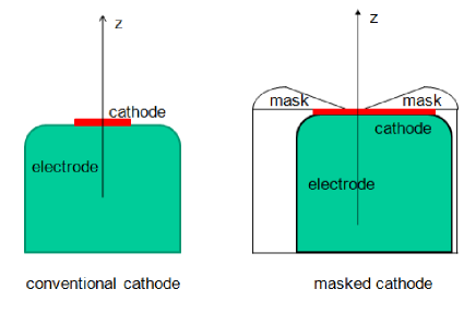
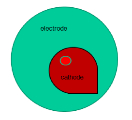
Figure 1 shows a schematic plot of the side view comparison of the conventional photocathode and the masked photocathode. In the conventional photocathode, the photocathode material is mounted onto an electrode made of conducting material such as . The photocathode surface facing the accelerating vacuum chamber will be exposed to the incident laser and also the back bombardment of ionized ions and multipacting electrons. In the masked photocathode, a mask electrode with a small hole is put in front of the photo emissive material. The size of the hole can be used to control the transverse size and the uniformity of the photo electron beam distribution. The transverse size of electron beam is normally on the order of millimeter. It is much smaller than the conventional size of the photocathode which is on the order of a few millimeters. This suggests that the size of the hole could be made as the same as the transverse electron beam size. Such a hole helps cut off tails from a large transverse size Gaussian laser beam and makes the electrons out of the hole more uniform. The mask electrode also protects the photocathode material from the bombardment damage of the ions and the electrons. It also prevents the dark current and the secondary electrons being generated from the photocathode surface. The size of the masked photocathode can be made relatively large (on the order of centimeter) with an axis different from the axis of the mask electrode. Figure 2 shows a top view of the masked photocathode. By rotating and moving the axis of the photocathode behind the mask electrode, the new photo emissive surface can be moved into the hole for generating electrons after the depletion of the active photo emissive material inside the hole. Since the surface area of the photocathode is an order of magnitude larger than the area of the hole, this means that an order of magnitude of new photocathode holes could be produced by simply moving the photocathode behind the mask electrode. This significantly shortens the time used for photocathode material replacement in the conventional photocathode. To move the photocathode behind the mask, the close contact between the photocathode and the mask electrode is released slightly. This will avoid the damage to the photo emissive surface due to the friction between the photocathode and the mask electrode during the process of motion.
III Beam Dynamics Simulations inside a Masked Photocathode Gun


The mask electrode provides a natural transverse cut-off to the incident Gaussian laser beam. From the beam dynamics point of view, this produce a more transversely uniform electron beam that helps reduce the emittance growth of the electron beam. As an illustration, we use an electrostatic gap described in the next section to study the effects of the masked cathode fields on the electron beam dynamics through the gun. Figure 3 shows the on-axis accelerating electric field with and without the mask electrode. The off-axis field distributions can be obtained from the derivatives of this on-axis field following the Maxwell’s equations and the azimuthal symmetry condition. Without the mask electrode, the peak of the electric field is on the photocathode surface. With the mask, the accelerating electric field on the photocathode inside the hole is reduced by a few percentage. The peak of the field is moved downstream. This generates a transverse field that might help focus the photo-electron beam.

Figure 4 shows the transverse projected emittance evolution through the gun with an initial transversely uniform distribution, Gaussian distribution, and truncated Gaussian distribution. In this example, we have used the masked electric field distribution in the Figure 3 with a maximum M/V field amplitude inside the gun. A solenoid is placed near the exit of the gun to provide emittance compensation. The electron beam has pC charge with a longitudinal uniform current distribution. The transverse rms size of the beam is mm. For the truncated Gaussian distribution, we assumed an initial beam rms size of mm that is the same as the mask hole aperture radius size. It is seen that the final projected rms emittance with the initial full Gaussian distribution is about a factor of two of the emittance with the initial uniform distribution due to the strong nonlinear space-charge forces from the Gaussian distribution. Using a larger laser spot size at the cathode with a mask hole truncates the initial Gaussian distribution. This provides a more uniform transverse distribution for electrons out of the hole. In above example, with mm rms transverse laser size, the final projected rms emittance of the beam is much less than the original full Gaussian distribution and is close to the emittance from the transversely uniform distribution.
To check the effects of masked cathode electric field on electron beam emittance, we also ran a comparison simulation using the masked electric field and the conventional no-mask electric field as shown in the Figure 3 with an initial transversely uniform distribution. The other parameters are the same as the ones used in the Figure 4. The projected rms emittance evolution inside the gun is given in Figure 5. There is no degradation of the beam emittance from the masked cathode field.
IV Discussions
Given the advantages of the masked photocathode described above, there could also exist some potential challenges with this cathode. First, the accelerating electric field on the photocathode surface will decrease due to the shielding of the mask electrode. To evaluate this problem, we used a simple model of two parallel plates with a static DC voltage to study the decrease of the field on the photocathode surface inside the hole. Figure 6 shows a schematic plot of computational geometry of the two-plate structure and contours of electric potential from the Poisson-Superfish calculation superfish .
Here, the mask electrode is tapered with a miminum thickness mm near the hole. The radius of the hole is mm. The distance between two plates is cm. Figure 7 shows the photocathode surface electric field normalized by the no-mask surface field as a function of the mask thickness at the hole with a fixed hole radius ( mm) and as a function of the hole radius with a fixed thickness ( mm).


It appears that accelerating field at the photocathode surface goes down quickly with the increase of the depth of the hole (i.e. the thickness of the mask). However, as long as the thickness of the mask can be controlled below mm, the accelerating field at the photocathode surface can still reach of the original surface field without the mask. Using a mm thick mask, the accelerating field at the photocathode surface can attain more than of the original field. With a larger hole radius as shown in the bottom plot of the figure, the accelerating field at the photocathode surface is larger due to the fact that more fields will be able to penetrate into the hole.
Putting the masked electrode in front of the photocathode might result in larger electric field on the surface of the mask electrode. Using above numerical example, we found that the maximum electric field on the mask surface is about higher than the electric field on the photocathode surface without mask. Whether this increased field will cause field emission dark current depends on the material used for the mask electrode and the amplitude of the electric field. Using a high work function material helps reduce the chance of dark current from the mask electrode surface. Coating the mask surface facing the accelerating vacuum chamber also helps lower the dark current. Recent report using nitrogen-implanted silicon oxynitride film to coat an electrode surface demonstrated order of magnitude improvement in suppressing the field emission theodore .
Another challenge to the masked photocathode is the potential damage to the photocathode due to the diffusion of the photo emissive material into the mask electrode because of the close contact between the photocathode and the back surface of the mask electrode. Such a problem could be overcome by using an electrode material (e.g. ) to minimize the interaction between the photo emissive material and the mask metal electrode. Another possible way to solve this problem is to coat the back surface of the mask electrode with the same photo emissive material as the photocathode.
From engineering point of view, to build the masked photocathode might require some extra efforts and cost. This includes building a mask electrode with very thin tip (below mm), and building a photocathode supporting electrode with the capability to move the cathode around. However, those extra efforts will be paid back by significantly improving the lifetime of the photocathode usage (in order of magnitude), and by improving the electron beam quality inside the photoinjector. Furthermore, such a masked photocathode might also be used to generate a flat beam for emittance exchange application by using a high aspect ratio rectangular opening hole.
Acknowledgements
We would like to thank Drs. D. Dowell, J. Corlett, R. Ryne, J. Staple, F. Sannibale, R. Wells, W. Wan, M. Zolotorev for useful discussions. This research was supported by the Office of Science of the U.S. Department of Energy under Contract No. DE-AC02-05CH11231. This research used resources of the National Energy Research Scientific Computing Center.
References
- (1) C. Hernandez-Garcia, “Present status and future of DC photoemission electron guns for high power, high brightness applications,” in High Brightness High Power Workshop UCLA, January 14-16 2009.
- (2) S. Lederer et al., in Proceedings of EPAC08, Genoa, Italy, p. 232 (2008).
- (3) C. Hernandez-Garcia et al., “Status of Jefferson Lab FEL high voltage photoemission guns,” in Workshop on Sources of Polarized Electrons and High Brightness Electron Beams, Jefferson Lab, NewPort News, VA, USA, Oct. 1-3, 2008.
- (4) B. L. Militsyn et al., in Proceedings of EPAC08, Genoa, Italy, p. 235 (2008).
- (5) S. Schreiber et al., in Proc. PAC 03, Chicago (USA), 2003.
- (6) J. Han, M. Krasilnikov, K. Flottmann, Phys. Rev. ST AB, 8, 033501 (2005).
- (7) J. Han, K. Flottmann, W. Hartung, Phys. Rev. ST AB, 11, 013501 (2008).
- (8) N. D. Theodore et al., IEEE Transactions on Plasma Science, vol. 34, 1074 (2006).
- (9) J.H. Billen, L.M. Young, POISSON SUPERFISH, Los Alamos National Laboratory report LA-UR-96-1834 (revision January 8, 2000).