Scalable Neutral Atom Quantum Computer with Interaction on Demand: Proposal for Selective Application of Two-Qubit Gate
Abstract
We propose a scalable neutral atom quantum computer with an on-demand interaction through a selective two-qubit gate operation. Atoms are trapped by a lattice of near field Fresnel diffraction lights so that each trap captures a single atom. One-qubit gate operation is implemented by a gate control laser beam which is applied to an individual atom. Two-qubit gate operation between an arbitrary pair of atoms is implemented by sending these atoms to a state-dependent optical lattice and making them collide so that a particular two-qubit state acquires a dynamical phase. We give numerical evaluations corresponding to these processes, from which we estimate the upper bound of a two-qubit gate operation time and corresponding gate fidelity. Our proposal is feasible within currently available technology developed in cold atom gas, MEMS, nanolithography, and various areas in optics.
1 Introduction
Quantum computation employs a quantum mechanical system as a computational resource [1, 2, 3]. It is expected that a large scale quantum computer outperforms its classical counterpart exponentially by making use of superposition states and entangled states. In spite of many proposals for potentially scalable quantum computers, most physical realizations so far accommodate qubits on the order of ten, at most. One of the obstacles against scalability in the previous proposals is the absence of controllable interaction between an arbitrary pair of qubits. Small scale quantum computers are already demonstrated experimentally in several physical systems, such as NMR, trapped ions, photons, and neutral atoms. These physical systems have merits and demerits and no single physical system to date satisfies all the DiVincenzo criteria, the necessary conditions for a physical system to be a candidate of a working quantum computer.[4]
A neutral atom quantum computer is one of the most promising candidates of a scalable quantum computer. Neutral atoms are believed to be robust against decoherence, another obstacle against a physical realization of a working quantum computer, since they are coupled very weakly to the environment. A one-qubit gate operation has been already demonstrated with a two-photon Raman transition,[5, 6] which is a well-established technique today. A two-qubit gate operation makes use of a cutting edge technique involving ingenious manipulation of hyperfine-state-dependent optical lattice potentials.[7, 8, 9, 10] A drawback of this two-qubit gate implementation is that the gate acts on all the nearest neighbor pairs in the optical lattice simultaneously. Hence a selective gate operation is yet to be realized, although some ideas utilizing optical tweezers has been proposed [11].
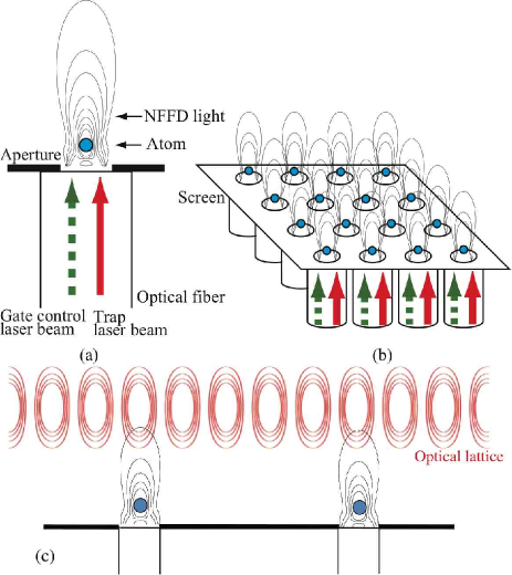
It is the purpose of the present paper to propose a new design of a neutral atom quantum computer with an on-demand interaction, which is potentially scalable up to a large number of qubits within currently available technology [12, 13]. The schematic illustration of our proposal is shown in Fig. 1. We punch an array of apertures in a thin substrate made of, e.g., silicon. An optical fiber is attached to each aperture, which lets in two laser beams, one for trapping and the other for one-qubit gate control. Atoms are trapped by a near field Fresnel diffraction light (NFFD) [14], which is produced by letting the trap laser light pass through an aperture with a diameter comparable to the wavelength of the laser, so that each trap holds a single atom. Turning on and off the trap laser individually is required to implement a selective two-qubit gate as will be shown later. Each lattice site is also equipped with its own gate control laser beam so that individual single-qubit gate operations can be applied on many qubits individually and simultaneously. A controlled two-qubit gate operation between an arbitrary pair of qubits is made possible by selectively transferring two atoms in a superimposed one-dimensional optical lattice and by employing the method demonstrated by Mandel et al [9]. Here, we give detailed analysis of the selective two-qubit gate implementation according to our proposal.
Technology required for physical implementation of the proposed quantum computer has already been developed in the areas of cold atom trap, scanning near field optical microscope (SNOM), nanolithography, and quantum optics, among others, and we believe there should be no obstacles against its physical realization.
We first briefly review the design of a neutral atom quantum computer demonstrated by Mandel et al. [9] in Sec. 2. We point out problems inherent in their design. Individual atom trap by making use of NFFD light is introduced in Sec. 3. Section 4 is devoted to one- and two-qubit gate implementations. We separate the two-qubit gate operation into several steps and evaluate the execution time and the corresponding fidelity of each step in Sec. 5 and AppendixA. Conclusion is given in Sec. 6.
2 Brief Review of Neutral Atom Quantum Computer in Optical Lattice
In this section, we look back the experiments by Mandel et al. [7, 8, 9] to give a basic background on how to trap and manipulate atoms using laser beams and how to implement gate operation. We subsequently point out problems inherent in their design.
Suppose an atom is put in a laser beam with an oscillating electric field , where is the laser frequency. It is assumed that is close to some transition frequency between two states and of the atom. The interaction between the electric field and the dipole moment of the atom introduces an interaction Hamiltonian
| (1) |
where is the dipole moment operator of the atom. This interaction introduces an effective potential of the form
| (2) |
for an atom in the ground state, which is called the AC Stark shift. Here , while is the detuning. We have ignored the small natural line width of the excited state. In case (blue-detuned laser), is positive and a region with large works as a repulsive potential. In contrast, if (red-detuned laser), is negative and a region with large works as an attractive potential. We use mainly a red-detuned laser in the following proposals.
It is possible to confine neutral atoms by introducing a pair of counterpropagating laser beams with the same frequency, amplitude and polarization along the -axis. These beams produce a standing wave potential, called an “optical lattice” of the form
| (3) |
where is the wave number of the laser and is the waist size, which is on the order of the laser wavelength. It is possible to construct a three-dimensional lattice by adding two sets of counterpropagating beams along the - and the -axes. Note that the lattice constant is always , where is the wavelength of the laser.
Mandel et al. trapped atoms in such an optical lattice [9]. They used the Rabi oscillation to implement one-qubit gates, in which a microwave (MW) field was applied. They have chosen qubit basis vectors and to be in harmony with the one-qubit gate operation making use of the Rabi oscillation.
For two-qubit gate operations, they introduced time-dependent polarization in the counterpropagating laser beams as
| (4) |
These counterpropagating laser beams produce an optical potential of the form
| (5) |
where () denotes counterclockwise (clockwise) circular polarization. Note that the first component () moves along the -axis as is increased, while the second component () moves along the -axis under this change [8]. The component introduces transitions between fine structures; , , and . The transitions from to are red-detuned, while the transition from to is blue-detuned if is chosen between the transition frequencies of and . Then by adjusting properly, it is possible to cancel the attractive potential and the repulsive potential associated with these transitions. The net contribution of the laser beam in this case is an attractive potential for an atom in the state . We denote this potential as in the following. Similarly, the component introduces a net attractive potential , through the transition on an atom in the state .
Mandel et al. [9] took advantage of these state-dependent potentials to implement a two-qubit gate. By applying the Walsh-Hadamard gate on , one generates a tensor product state . The potentials acting on the states and are evaluated as
| (6) |
By decreasing the phase , the state moves with dominating toward -direction, while moves with toward -direction. Thus it is possible to make and collide between the two lattice points. If they are kept in the common potential well during , the subspace obtains a dynamical phase [7], where is the on-site repulsive potential energy. After these two components spend in the potential well, they are brought back to the initial lattice point by reversing , which results in the two-qubit gate operation
| (7) |
It should be noted, however, that the state dependent potentials act on all the pairs of the atoms and selective operation of the two-qubit gate on a particular pair is impossible. Their proposal may be applicable to generate a highly entangled state for a cluster state quantum computing, although it is not applicable for a circuit model quantum computation.
In the following sections, we propose implementations of a neutral atom quantum computer, which overcome these difficulties.
3 Near Field Fresnel Diffraction Trap
Suppose there is an array of apertures in a thin substrate. We consider a square lattice of apertures for definiteness. The substrate is made of a thin silicon, for example. Silicon has a very good thermal conductivity, comparable to a metal, and local heating due to a laser is expected to diffuse quickly. It is possible to maintain the substrate in a low temperature if the perimeter of the substrate is in contact with a refrigerator, which suppresses thermal excitation of an atom.
Bandi et al. [14] proposed to trap an atom with a microtrap employing NFFD light. Atoms are trapped in an array of NFFD traps, each of which traps a single atom. An NFFD light is produced if a plane wave with the wave length is incident to a screen with an aperture of the radius . The ratio is called the Fresnel number. The trap potential is evaluated by applying the Rayleigh-Sommerfeld formula as
| (8) |
where
| (9) |
and
| (10) |
with the distance between and in the plane. Here, is half of the spontaneous decay rate, the amplitude of the incoming plane wave, its wave number, the detuning is negative (red-detuned), and the plane wave is incident to a screen from the -axis. The integral is over the aperture region .
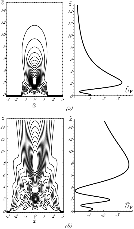
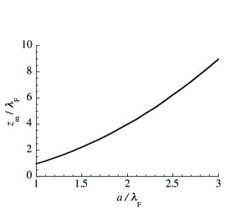
The aperture size is on the order of the wave length so that the distance between the minimum of the potential energy and the substrate is on the order of the wavelength. Figure 2 shows the trap potential profiles for two aperture radii, which is obtained by evaluating Eq. (8) numerically. It is clear from Fig. 2. that the distance between the atom and the substrate is controllable by manipulating the aperture size . Figure 3 shows the -coordinate of the potential minimum () as a function of the aperture size . We take advantage of this fact in our implementation of a two-qubit gate later.
The aperture size may be controlled by employing a small scale liquid crystal technology called Spatial Light Modulator (SLM) with Liquid Crystal on Silicon (LCOS) technology [15, 16]. An array of shutters made of liquid crystal may be fabricated on a silicon wafer with LCOS-SLM. The current operation time of the SLM is reported to be sub msec, which is comparable to the operation times of the other steps in our gate implementation discussed below. Alternatively, well-established Micro-Electro-Mechanical Systems (MEMS) technology may be employed to control the aperture radius. An MEMS shutter for a display is already in a mass production stage [17] and it may be applied to demonstrate our proposal. The on (off) switching time of the shutter is 54 (36) s [17] and we expect even faster switching time by optimizing its structure for our purpose [18].
It is clear by construction that we have freedom in the choice of the lattice constant and the lattice shape. We may even arrange the traps in an irregular form if necessary. This is a remarkable new feature, which a conventional two-dimensional optical lattice cannot provide with; an optical lattice is always regular and its lattice constant is on the order of the wavelength of the laser beams, where the lattice constant can be tuned to some extent by changing the angle of two lasers [19].
4 Quantum Gate Implementations
For a quantum system to be a candidate of a general purpose quantum computer, it is necessary for the system to be able to implement a universal set of quantum gates, that is, the set of one-qubit gates and almost any two-qubit gate [20]. Now we explain how these gates are realized in our proposal.
In the following we take two hyperfine states to represent two-qubit basis vectors, which we denote and . The hyperfine states must be consistent with two-qubit gate operations and we take, for definiteness, and throughout this paper.
4.1 One-Qubit Gates
Let us assume, for definiteness, the NFFD trap potential is strong enough so that there is only one atom in each trap. Along with the NFFD trap light, there is a gate control laser beam propagating through the fiber, which is depicted in a broken line in Fig. 1.
One-qubit gate is implemented by making use of the two-photon Raman transition [3], which is already demonstrated [5, 6]. Let and be the energy eigenvalues of the states and , respectively, and let be the energy eigenvalue of an auxiliary excited state necessary for the Raman transition. Suppose that a laser beam with the frequency has been applied to the atom. Let be the detuning and be the Rabi oscillation frequency between the state and . Then, under the assumptions , we obtain the effective Hamiltonian
| (11) |
where
Note that generates all the elements of SU(2) since there are two generators in the Hamiltonian and their coefficients are controllable.
4.2 Two-Qubit Gates
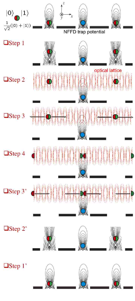
As illustrated in Fig. 4, our proposal for selective two-qubit gate operation consists of 7 steps:
-
1
We choose two trapped atoms to be operated by the gate. Each atom is made into a superposition state by a gate control laser beam attached to each aperture. Then, these atoms are transferred from the vicinity of the substrate to space coordinates, where a one-dimensional optical lattice will be introduced later, by enlarging the aperture radius. The minima of the optical lattice will be situated at these space coordinates.
-
2
While the atoms stay at the points, the NFFD lasers of the two atoms are gradually turned off while a pair of counterpropagating laser beams to form an optical lattice is gradually turned on.
-
3
Now the two atoms are trapped in the optical lattice. As described in Sec. 2, the polarizations of the pair of the counterpropagating laser beams are rotated in opposite directions so that the qubit state is transferred toward positive -direction, while is transferred toward negative direction. Therefore, it is possible to collide of one atom and of the other atom.
-
4
Now, component of one atom and of the other are trapped in the same potential well in the optical lattice. They interact with each other for a duration so that this particular state acquires an extra phase compared to other components , and . Here is the on-site interaction energy with the atomic mass and the -wave scattering length . When satisfies the condition , we obtain a nonlocal two-qubit gate . Application of further one-qubit gates implements a CNOT gate or a CZ gate.
-
3’
After acquiring the phase, two atoms are separated along the optical lattice by an inverse process of Step 3.
-
2’
Atoms are transferred from the optical lattice to the NFFD trap by an inverse process of Step 2.
-
1’
Aperture radii of NFFD lasers are reduced so that the atoms are transferred back to the vicinity of the substrate by an inverse process of Step 1. Now the gate operation is completed.
5 Execution Time of Two-Qubit Gate
In this section, we analyze all steps of selective two-qubit gate operation in detail one by one to estimate the execution time. While shorter execution time is preferred, the fidelity should be kept close to 1 during the gate operation. The fidelity is mostly bounded by adiabaticity requirement. Here, we give an estimate of the execution time, which is limited by the adiabatic condition. Detailed numerical simulations, using the time-dependent Schrödinger equation with experimentally realistic parameters, for each step will be described in Appendix A.
5.1 Step 1
Suppose that an atom is transferred away from the vicinity of the substrate (from to ) by increasing the aperture radius , e.g. from (a) to (b) of Fig. 2. The distance may be a few times of . As seen from Fig. 2, the NFFD trap potential in this parameter range is shallow along the -axis and steep in the xy-plane, which means that the curvature along the -axis dominates the adiabaticity condition. The angular frequency along the -axis around the minimum is
| (12) |
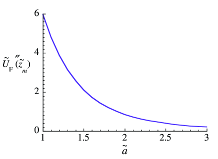
where we put tildes for dimensionless variables scaled by the wavelength and the potential amplitude of the NFFD trap Eq. (8); is the characteristic time scale for NFFD trap and . The dimensionless curvature as a function of the aperture size is shown in Fig. 5.
Since is a monotonically decreasing function of , the characteristic time for an adiabatic change can be estimated from the condition
| (13) |
which gives
| (14) |
Here we have taken the “worst” curvature at the final value of , i.e., . For the typical parameter values for a realistic NFFD trap (see AppendixA.1) we can see , because the depth of the NFFD trap is very deep. We expect, from this estimation, that the transfer of an atom from the initial position to the optical lattice potential minimum will be bounded in time by .
5.2 Step 2
Now that the atoms are transferred to the right space points, their wavefunctions must be transformed from the ground states of the NFFD traps to those of the optical lattice adiabatically. It is important to note that the centers of the NFFD traps and those of the optical lattice potential must be sitting at the same space points for a smooth transfer of atoms. The adiabaticity in this case is limited by the smallest potential curvature, that is, the curvature of (Eq. (3)) along the radial ( or ) direction, because the typical laser waist satisfies . The separation between the ground state and the first excited state energies gives a time scale , where the angular frequency is defined as
| (15) |
Using the typical time scale with the recoil energy of the optical lattice, the time scale is expressed as
| (16) |
which gives a time scale s for typical parameter values (Appendix A.2).
5.3 Step 3
Now, the atoms are trapped in the state-dependent optical lattice. According to our construction, the length between two nearest-neighbor apertures in the substrate is larger than a few times of the wavelength of laser beams. Then it is difficult to load two atoms in the nearest neighbor minima of the optical lattice, because the lattice constant is . To collide the atoms, we must move the () atom right (left) by , if the initial separation between the two atoms is ; may be more than 5.
The rough estimate of the execution time can be obtained by considering the adiabatic transport by one lattice constant along the -axis in the usual optical lattice Eq. (3). The adiabaticity condition is then given by . Thus, the adiabatic time scale for the motion with lattice constant is estimated as
| (17) |
where has been defined in Step 2.
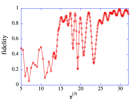
In our choice of the hyperfine states for and , the state-dependent lattice potentials are given by Eq. (29) in AppendixA. They are superpositions of two counterpropagating plane waves and there is an interference between them. Then, the simple adiabatic argument cannot apply to this situation. Actually, as shown in AppendixA, the fidelity is an oscillating function of the operation time for a given ; in other words, the adiabaticity time is not a monotonous function of . We find through the numerical simulation that the execution time is roughly a few tens of the typical time scale .
5.4 Step 4
Let be the ground state wave function of an atom in one of the optical lattice potential wells . If two atoms in the ground state are put in the same potential well, the interaction energy is given by
| (18) |
To acquire a phase necessary for the controlled- gate, for example, these atoms must be kept in the same potential well for .
For the -wave scattering length nm between two 87Rb atoms in and [21] and typical parameters of the optical lattice (see AppendixA), we find of a few msec, which is the largest execution time among all the steps. This step does not involve any nonadiabatic process and we believe the operation is executed with a high fidelity by fine tuning the holding time .
5.5 Step 3’, 2’ and 1’
It is clear that Step ’ is an inverse process of Step and time required for and the fidelity of the inverse process are the same as those for a forward process. The mathematical proof is described in AppendixB.
5.6 Total execution time and fidelity
We have estimated the time required for each step, under the assumption that each step gives a fidelity close to 1. The overall execution time of a two-qubit gate is given by . The rough estimate under the adiabaticity condition gives 10 ms. Through the numerical simulation of the Schrödinger equation with realistic parameters, as shown in AppendixA, we obtain msec.
The overall fidelity is estimated as follows. Each of Steps 1, 2, 3, 3’, 2’ and 1’ involves two independent processes. For example, sending an atom from the vicinity of the substrate to the space point in Step 1 is realized with the fidelity 0.99 for each atom. Since this step involves two atoms, the fidelity associated with this step must be . Thus the overall fidelity is , where we assumed that the interaction time is tunable so that Step 4 gives a fidelity arbitrarily close to 1. The fidelity may be improved by spending more time for each step.
Execution time may be shortened by applying stronger laser fields, because the separation between neighboring energy levels is enlarged by this, which makes fast adiabatic operation possible. Besides, stronger laser fields suppress tunneling of an atom in the optical lattice to the adjacent potential minima. The ground state wave function is squeezed in a stronger lattice potential well, leading to a larger value of . Then, Step 4 is also executed in a shorter time. To make this statement more concrete, let us make a harmonic approximation to the potential well of the optical lattice. One can see that is reduced by a factor if is made larger; for example, is multiplied by if becomes 10 times larger. We expect that overall execution time can be reduced by one order of magnitude by employing laser beams which are ten times stronger than the current value.
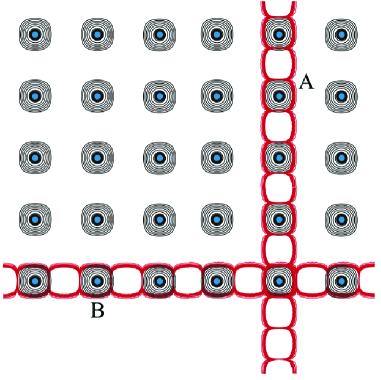
In case the two atoms are in a general position, not necessarily along a primitive lattice vector of the optical lattice, we may introduce two orthogonal optical lattices as shown in Fig. 6 (a). Then the selected atomic states of one atom and of the other meet at the intersection of the two optical lattices to acquire the extra dynamical phase. It should be noted that two-qubit gate operations may be applied simultaneously and independently on many pairs of qubits.
6 Conclusion
We proposed a scalable design of a neutral atom quantum computer with an on-demand interaction. A qubit is made of two hyperfine states of an atom. Associated with each atom, there is an optical fiber, through which a trap laser and a gate control laser are supplied. The latter is used to implement one-qubit gates by two-photon Raman transitions. We have shown that a selective two-qubit gate operation is possible if atoms are trapped by an array of NFFD traps with a variable aperture size. This would allow for true two-qubit gates, rather than performing the same gate operation with many atoms in massive parallelism as in the experiments by Mandel et al [9]. We have obtained an upper bound of the gate operation time of 7.87 ms with the corresponding fidelity of 0.886. It may be possible to further reduce the execution time or increase the fidelity by taking different time-dependence of the control parameters. Reduction of the gate operation time is also possible by increasing the laser intensity.
We believe that most of our proposal can be demonstrated within current technology. The severe technical challenge is to attach the ends of the optical fibers to the apertures of the substrate. We strongly believe that the rapid progress in nanotechnology makes it possible to solve this in the foreseeable future. Some other issues, such as trapping atoms near material surfaces, how to form an optical lattice in close proximity to a surface, and how to load individual traps with single atoms, should be addressed seriously toward realization of our proposal. We plan to study these issues in the future and would like to encourage experimentalists to design experiments based on our proposal.
Acknowledgements.
One of the authors (M.N.) would like to thank Takuya Hirono for drawing his attention to [21] and Yutaka Mizobuchi for discussions. We are also grateful to Ken’ichi Nakagawa for enlightening discussions. A part of this research is supported by “Open Research Center” Project for Private Universities: Matching fund subsidy from MEXT (Ministry of Education, Culture, Sports, Science and Technology). K.K. is supported in part by Grant-in-Aid for Scientific Research (Grant No. 21740267) from the MEXT of Japan. Y.K., M.N. and T.O. are partially supported by Grant-in-Aid for Scientific Research from the JSPS (Grant No. 23540470).Appendix A Numerical Simulations of Two-Qubit Gate Operation
The purpose of AppendixA is to estimate the execution times of Steps 1 through 3 in the two-qubit gate operation introduced in Sec. 4.2 by solving the time-dependent Schrödinger equation
| (19) |
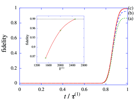
numerically. Using the experimentally relevant parameters, we calculate the optimized time to implement the gate operation keeping the fidelity 0.99 for each step. Here, the fidelity is defined as the overlap between the ground state wavefunction at the final potential configuration in Steps 1, 2 and 3 and the solution of Eq. (19):
| (20) |
A.1 Step 1
A red-detuned laser beam passing through an aperture with a radius on the order of the laser wavelength forms an attractive potential of Eq. (8) to an atom. The potential profile is a function of time if the aperture radius changes as a function of time. We solve Eq. (19) with numerically to evaluate the time required to transfer an atom from the vicinity of an aperture to a space point, which will be a minimum of an optical lattice potential when it is turned on.
We use the D1 transition of 87Rb atom to trap an atom and take the numerical values
| (21) |
for the relevant parameters for definiteness, where the laser intensity is put to W/cm2 [14]. Here is the wavelength of the trap laser and is the potential depth. The wavelength is fixed through the detuning
| (22) |
where nm is the wavelength of the D1 transition [21]. With these parameters, the lifetime of atoms due to the photon recoil heating is given as sec with the recoil energy and the photon scattering rate , which is much longer than the total execution time.
We rewrite the Schrödinger equation in a dimensionless form using the values given in (21), and introduce the cylindrical coordinates by taking advantage of the cylindrical symmetry around the -axis. By writing , the Schrödinger equation is put in the form
| (23) |
where dimensionless variables are denoted with a tilde and .
We take the initial aperture radius , corresponding to , and the final aperture radius , for which , in our computation [see Fig. 2]. Let be the dimensionless time required to change the aperture size from to . The aperture size is changed as
| (24) |
Here, we have vanishing initial and final velocities to avoid oscillatory behavior of the wave function during time evolution.
A.2 Step 2
We switch from the NFFD potential to the optical lattice potential with the time scale as
| (25) |
to this end. Here is the NFFD trap potential at and
| (26) |
is the optical lattice potential, where is the -coordinate of the minimum of the NFFD potential at .
It turned out to be convenient to employ different scaling for physical parameters here from those in Step 1. We use scales
| (27) |
and a dimensionless variable is denoted with a tilde as before.
Now the Schrödinger equation (19) is put in a dimensionless form as
| (28) |
For definiteness, we take and . We have taken to be of the same order as that in Mandel et al [9]. It should be noted that there is no rotational symmetry in the above Schrödinger equation and it must be solved by using the Cartesian coordinate system.
A.3 Step 3
The optical transitions shows that the effective potentials acting on and are
| (29) |
respectively. Here, we use the following decompositions
| (30) |
where in the right hand side denotes a vector with nuclear spin and electron spin , for example. If the polarization angle is increased, () moves right (left). The choice of these hyperfine states gives an exactly counter-moving potential Eq. (29) for and , while the states used by Mandel et al. [9] yield the asymmetric potential given in Eq. (6). Hence we restrict ourselves to the motion of state below.
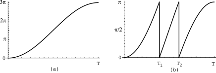
We take the number of the lattice constant over which an atom is transported to be . In actual experiments, the angle may be changed by using an electro-optic modulator (EOM). The angle is then limited within the range . This means that we have to reset to zero as soon as it reaches to , if we need to change beyond (Fig. 8). The trick is that even when jumps by , does not change at all. This reset must be done instantaneously so that the trapped atoms does not move in the optical lattice during the resetting time. By repeated use of this reset times, it is possible to change effectively from to .
We have solved the Schrödinger equation
| (31) |
numerically. The angle is changed as
| (32) |
in case an atom is transferred in the optical lattice by site. We employ the same scaling as introduced in Step 2, with which the Schördinger equation is put into a dimensionless form as
| (33) |
Here, we use the cylindrical coordinates by taking advantage of the cylindrical symmetry of the optical lattice around the -axis.
The Schrödinger equation is solved numerically and we find that the operation time , which gives the fidelity 0.99, is 0.577 ms and 1.28 ms for two choices and , respectively. Note that is not a monotonous function of . This is due to the fact that the lattice potentials and are superpositions of two counterpropagating plane waves and there is an interference between them. In fact, the fidelity is an oscillating function of for a given ; an example is shown in Fig. 9. These complicated properties make the execution time several times longer than the time scale obtained from adiabaticity requirement in Sec. 5.3.
Appendix B Equivalence of and
Let and be the eigenstates of the Hamiltonian at and , respectively. Under the potential change , and hence the Hamiltonian change , the state develops as
| (34) |
The fidelity of this process is defined as
| (35) |
For the reverse process , we start with . The time development operator is . Then the fidelity is
| (36) | |||||
where the reality of is used.
References
- [1] Quantum Information Science and Technology Roadmapping project; http://qist.lanl.gov/
- [2] M. A. Nielsen and I. L. Chuang: Quantum Computation and Quantum Information (Cambridge University Press, Cambridge 2000).
- [3] M. Nakahara and T. Ohmi: Quantum Computing: From Linear Algebra to Physical Realizations (Taylor & Francis, 2008).
- [4] D. P. DiVincenzo: Fortschr. Phys. 48 (2000) 771.
- [5] D. D. Yavuz, P. B. Kulatunga, E. Urban, T. A. Johnson, N. Proite, T. Henage, T. G. Walker, and M. Saffman: Phys. Rev. Lett. 96 (2006) 063001.
- [6] M. P. A. Jones, J. Beugnon, A. Gaëtan, J. Zhang, G. Messin, A. Browaeys, and P. Grangier: Phys. Rev. A 75 (2007) 040301(R).
- [7] D. Jaksch, H.-J. Briegel, J. I. Cirac, C. W. Gardiner, and P. Zoller: Phys. Rev. Lett. 82 (1999) 1975.
- [8] O. Mandel, M. Greiner, A. Widera, T. Rom, T. W. Hänsch, and I. Bloch: Phys. Rev. Lett. 91 (2003) 010407.
- [9] O. Mandel, M. Greiner, A. Widera, T. Rom, T. W. Hänsch, and I. Bloch: Nature (London), 425 (2003) 937.
- [10] P. Treutlein, T. Steinmetz, Y. Colombe, B. Lev, P. Hommelhoff, J. Reichel, M. Greiner, O. Mandel, A. Widera, T. Rom, I. Bloch, and T. W. Hänsch: Fortschr. Phys. 54 (2006) 702.
- [11] R. Stock, N. S. Babcock, M. G. Raizen, and B. C. Sanders: Phys. Rev. A 78 (2008) 022301; N. S. Babcock, R. Stock, M. G. Raizen, B. C. Sanders: Can. J. Phys. 86, (2008) 549; C. Weitenberg, S. Kuhr, K. Mølmer, J. F. Sherson: arXiv:1107.2632.
- [12] A basic idea of our proposal without quantitative discussion was reported in M. Nakahara, T. Ohmi, Y. Kondo: arXiv:1009.4426 (unpublished).
- [13] A selective two-qubit gate has been discussed in L. Banchi, A. Bayat, P. Verrucchi, and S. Bose: Phys. Rev. Lett. 106 (2011) 140501 by employing proposal introduced in Ref [12]. The difference between our proposal and theirs is that qubits in the NFFD trap are selectively interacted with atoms in the Mott insulator regime in their proposal.
- [14] T. N. Bandi, V. G. Minogin, and S. N. Chormaic: Phys. Rev. A 78 (2008) 013410.
-
[15]
http://sales.hamamatsu.com/en/products/solid-state-division/lcos-slm.php&src=hp - [16] T. Inoue, H. Tanaka, N. Fukuchi, M. Takumi, N. Matsumoto, T. Hara, N. Yoshida, Y. Igasaki, and Y. Kobayashi: Proc. SPIE 6487 (2007) 64870Y.
-
[17]
http://www.pixtronix.com/ -
[18]
http://www2.electronicproducts.com/MEMS_shutter_array_to_revolutionize_optoelectronics-article-SEPOL1-SEP2003.aspx - [19] S. Peil, J. V. Porto, B. L. Tolra, J. M. Obrecht, B. E. King, M. Subbotin, S. L. Rolston, and W. D. Phillips: Phys. Rev. A 67 (2003) 051603(R); Z. Hadzibabic, S. Stock, B. Battelier, V. Bretin, and J. Dalibard: Phys. Rev. Lett. 93 (2004) 180403.
- [20] A. Barenco, C. H. Bennett, R. Cleve, D. P. DiVincenzo, N. Margolus, P. Shor, T. Sleator, J. A. Smolin, and H. Weinfurter: Phys. Rev. A 52 (1995) 3457.
- [21] A. M. Kaufman, R. P. Anderson, T. M. Hanna, E. Tiesinga, P. S. Julienne, and D. S. Hall: Phys. Rev. A 80 (2009) 050701(R).