Band structure of hydrogenated Si nanosheets and nanotubes.
Abstract
The band structure of fully hydrogenated Si nanosheets and nanotubes are elucidated by the use of an empirical tight-binding model. The hydrogenated Si sheet is a semiconductor with indirect band gap of about eV. The symmetries of the wave functions allow us to explain the origin of the gap. We predict that, for certain chiralities, hydrogenated Si nanotubes represent a new type of semiconductor, one with co-existing direct and indirect gaps of exactly the same magnitude. This behavior is different from the Hamada rule established for non-hydrogenated carbon and silicon nanotubes. Comparison to an ab initio calculation is made.
1 Introduction
Graphene exhibits electronic properties that conventional metals do not show, e.g., charge carriers with zero effective mass, anomalous quantum Hall effect, and a minimum conductivity when carrier concentrations tend to zero [1]. The unconventional electronic properties of graphene occur due to its linear energy dispersion in the vicinity of the Dirac point and two-dimensional structure [1, 2]. Recent theoretical studies show, however, that a linear energy dispersion relation is not unique to graphene [3, 4, 5, 6]. For instance, a flat two-dimensional silicon (Si) sheet with a honeycomb lattice (silicene) exhibits a linear energy dispersion too [3, 4, 5, 6]. Even buckling of the Si honeycomb lattice (Si tends to form bonds rather than bonds) does not remove the linearity in the energy dispersion relation nor does it open an energy gap [3]. More generally, it has been predicted that a group-IV nanosheet with a flat or buckled honeycomb lattice also shows a linear dispersion too [4, 5, 6, 7]. It is the underlying symmetries of the honeycomb lattice that are responsible for the linear energy dispersion [3]. One-dimensional carbon nanostructures also exhibit unconventional electronic properties, e.g., carbon nanotubes show different electronic behavior depending on their chirality. Similarly to graphene, the unconventional electronic properties are not unique to carbon nanotubes [3, 8]. Si nanotubes also show electronic properties that are chirality dependent [3, 8].
The theoretical studies mentioned above motivated the experimental realization of two-dimensional sheets other than graphene. Silicon hexagonal sheets were chemically exfoliated from calcium disilicide (CaSi2) [9] and Si nanoribbons have been recently synthesized [10, 11, 12]. There is a report of the observation of a linear electronic dispersion for the Si nanoribbons using angle-resolved photoemission spectroscopy [13].
Similarly to graphene, there is interest in modifying a silicene sheet in order to tailor its properties. For example, studies have shown that Si nanoribbons can display semiconducting and magnetic behavior [4, 14]. Hydrogenation of silicene can also open a gap (e.g., hydrogenated graphene (graphane) is an insulator of direct band gap [15, 16]) and the resulting compound should be related to polysilane [17]. There are already a few ab initio calculations of related structures. Indeed, density functional theory (DFT) calculations within the local density approximation (LDA) found that a Si sheet without hydrogen is a semiconductor of gap zero [7]. Upon hydrogenation, the Si sheet becomes an semiconductor of indirect band gap [7, 17]. As for hydrogenated Si nanotubes, a previous density functional tight-binding theory found that hydrogenated Si nanotubes are semiconductors with a gap that shows little dependence on chirality [18].
It is the purpose of the present work to study the band structure of hydrogenated Si nanosheets and nanotubes in more detail than had been done previously with the ab initio method. In particular, () previous work had focused on structures, () the calculations of the hydrogenated Si sheet were all done using LDA, which suffers from the band-gap problem, () a discussion of the wave functions was missing from the earlier work, and () a complete study of the band structures of Si-H nanotubes has not yet been carried out. The most appropriate model is the empirical tight binding one.
In this paper, we will first consider a hydrogenated Si sheet (also referred as silicane [7]). For the hydrogenated Si sheet, we find that () it is an semiconductor of indirect band gap of about eV; () the lowest point of the conduction bands (CB) occurs at the M point and the highest point of the valence bands (VB) occurs at the point; () the indirect gap is closely related to the band structure of silicene and it is mainly due to band-filling effect; () the degeneracy at the Dirac point is not lifted by hydrogenating the Si sheet. We then consider the electronic structure of hydrogenated single-walled Si nanotubes (Si-H NTs). We find that () Si-H NTs of certain chiralities are semiconductors with co-existing direct and indirect gaps of identical magnitudes; () the magnitude of the gaps is equal to that of the hydrogenated Si sheet.
2 Tight-binding model of hydrogenated Si sheets
We now describe our tight-binding model. We consider a Hamiltonian with the following Bloch states for Si ( site),
| (1) |
and similarly for the sites and for H ( and sites). Here are Löwdin orbitals; is a lattice vector of the hexagonal lattice; is the position vector of the Si and H atoms in the unit cell; and is the number of unit cells. For Si atoms, we consider first nearest neighbors located at
and second nearest neighbors located at
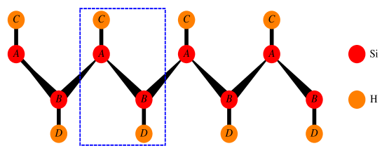
Here, is the buckling height; is the Si-H bond length; and Å is the lattice constant. These structural parameters are taken from ab initio calculations [7]. The origin is placed at site A (figure 1). For the hydrogen atoms, we only consider up to first-nearest-neighbor interactions. We further assume that there is only a bond between the Si and H atoms. Silicane has a hexagonal lattice with a basis composed of two Si atoms and two hydrogen atoms (figure 1).

Our tight-binding model is constructed as follows: () the Si-Si TB parameters are taken from those of bulk Si ( configuration); () the Si-H TB parameters are obtained by using the universal Harrison scaling rule [19] () the two-center approximation is used to account for the slight distortion of the hydrogenated sheet from pure hybridization. A simple and fairly good parametrization of the bulk Si structure is that of Grosso et. al. [20]. These parameters reproduce fairly well the band structure of bulk Si, in particular in the K direction, which is important for the Si nanosheets [3]. The full list of TB parameters is given in table 1.
3 Results and Discussion
We now present the results obtained from our tight-binding model. We first discuss the hydrogenated Si sheet. The hydrogenated Si sheet is an semiconductor with indirect gap eV (figure 2). Our result is in between the eV and eV reported previously [7, 17, 18]. The lowest point of the CB is at M and it is one-fold degenerate (figure 2 and table 2). The wave function at the M point of the lowest CB is given as follows (table 2): (%), (%), (%), and (%). The highest point in the VB is at and it is two-fold degenerate (figure 2 and table 2). The wave functions at the point of the highest VB is pure or pure (table 2). This is the same as was found for graphane [21].

|
The symmetries of the wave functions at , M, and K for the hydrogenated Si sheet are given in table 2. Note that the K point () is two-fold degenerate (table 2). This is expected since fully hydrogenating the Si sheet does not break the mirror symmetry of the honeycomb lattice. Another interesting result is that there is little hydrogen orbital () in the VB. Thus, the gap “opening ” is, in reality, due to the hydrogen electrons filling up the originally empty lowest CB of silicene; i.e., the gap is mostly intrinsic to silicene.
Next, we compare the band structures of graphane and silicane. The band structures of graphane and silicane differ significantly. First, graphane is an insulator of direct band gap [15, 16]. The gap occurs at . Second, the band gap of graphane (eV) is far larger than that of silicane [16]. This is expected since the C-C bond length in graphane is greater than the Si-Si bond length of silicane [7, 15].


We now consider the band structure of Si-H NTs. Si-H NTs are fully characterized by the chiral vector , where are integer numbers [22]. The band structure of Si-H NTs is obtained from that of silicane by quantizing the wave vector along the chiral direction [22].
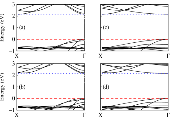
Armchair (,) and zig-zag (,) Si-H NTs with even have concurrent and identical direct and indirect gaps equal to that of the hydrogenated Si sheet (eV) (figure 3 (a) and (c)). We note that this dual behavior is different from the so-called mixed character previously reported [17] as the latter was for a nanosheet and was an approximate phenomenon. Armchair (,) and zig-zag (,) Si-H NTs with odd have direct gap equal to that of the hydrogenated Si sheet (figure 3 (b) and (d)). Therefore, Si-H NTs are semiconductors with either direct gaps, or with co-existing direct and indirect gaps of identical magnitude.
The electronic behavior of Si-H NTs is explained as follows. We first consider armchair Si NTs. For armchair Si-H NTs , quantization of the wave vector along the chiral direction gives their Brillouin zone (BZ) [22],
| (2) |
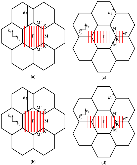
where, and . Armchair (,) Si-H-NTs with even have simultaneous and identical direct and indirect gaps since their BZ, equation (2), always crosses M and M’ (figure 4 (a)),
Armchair (,) Si-H NTs with odd have only a direct gap since their BZ always crosses M but not M’ (figure 4 (b)).
We now consider zig-zag Si-H NTs. For zig-zag Si-H NTs , quantization of the wave vector along the chiral direction gives their BZ [22],
| (3) |
where, and . Zig-zag (,) Si-H NTs with even have simultaneous and identical direct and indirect gaps since their BZ, equation (3), always crosses M, M’ and M” (figure 4 (c)),
Zig-zag (,) Si-H NTs with odd have only direct gap since their BZ always crosses M” but not M, M’ (figure 4 (d)). The above results on the gap dependence on chirality are much more complex than the Hamada rule [23] obeyed by non-hydrogenated carbon and silicon nanotubes [3].
We now compare our Si-H NTs results to those of Ref. [18]. Ref. [18] presents density functional tight-binding (DFTB) calculations of the Si-H NT gap. The DFTB calculation finds that Si-H NTs are semiconductors whose gap has little dependence on chirality. The gap of Si-H NTs rapidly converges to the gap of their hydrogenated Si sheet ( eV). No reference is made as to whether the gap is direct or indirect. Even though the electronic behavior of our TB model is in fairly good agreement with that of DFTB, one important difference is that our TB calculation did not find a dependence of the size of the gap at all. We attribute this difference to curvature effects, which are neglected in our model.
4 Conclusions
In summary, we performed a tight-binding calculation of the band structure of fully hydrogenated Si nanostructures. For the hydrogenated Si sheet (silicane), we find that it is a semiconductor with indirect band gap of about eV. The indirect band gap occurs between the M and points. Our study of the wave functions reveals that the gap is closely related to the band structure of silicene and is primarily due to a band-filling effect rather than to a gap opening. For Si-H NTs, we find that they are semiconductors with either a direct gap or with co-existing direct and indirect band gaps depending on chirality. Therefore, Si-H NTs do not follow Hamada’s rule. This shows that hydrogenated Si nanotubes can have properties distinct from carbon nanotubes.
References
References
- [1] Novoselov K S, Geim A K, Morozov S V, Jiang, D, Katnelson M I, Grigorieva I V, Dubonos S V, Firsov A A 2005 Nature 438 197.
- [2] Castro Neto A H, Guinea F, Peres N M R, Novoselov K S, Geim A K (2009) Rev. Mod. Phys. 81 109
- [3] Guzmán-Verri G G, Lew Yan Voon L C 2007 Phys. Rev. B 76 075131
- [4] Cahangirov S, Topsakal M, Akturk E, Şahin H, Ciraci S 2009 Phys. Rev. Lett. 102 236804
- [5] Şahin H, Cahangirov S, Topsakal M, Bekaroglu E, Akturk E, Senger R T, Ciraci S 2009 Phys. Rev. B 80 155453
- [6] Lebègue S, Eriksson O 2009 Phys. Rev. B 79 115409
- [7] Lew Yan Voon L C, Sandberg E, Aga R S, Farajian A A 2010 Appl. Phys. Lett. 97 163114
- [8] Durgun E, Tongay S, Ciraci S 2005 Phys. Rev. B 72 075420
- [9] Nakano H, Mitsouka T, Harada M, Horibuchi K, Nozaki H, Takahashi N Nonaka T, Seno Y, Nakamura H 2006 Angew. Chem. 118 6451
- [10] Kara A, Léandri C, Davila M E, De Padova P, Ealet B, Oughaddou H, Aufray B, Lay G L 2009 J. Supercond. Nov. Magn. 22 259
- [11] Kara A, Vizzini S, Léandri C, Ealet B, Oughaddou H, Aufray B, Lay G L 2010 J. Phys. C 22 045004
- [12] Aufray B, Kara A, Vizzini S, Oughaddou H, Léandri C, Ealet B. Lay G L 2010 Appl. Phys. Lett. 96 183102
- [13] De Padova P, Quaresima C, Ottaviani C, Sheverdyaeva P M, Moras P, Carbone C, Topwal D, Olivieri B, Kara A, Oughaddou H, Aufray B, Lay G L 2010 Appl. Phys. Lett. 96 261905
- [14] Ding Y, Ni J 2009 Appl. Phys. Lett. 95 083115
- [15] Sofo J O, Chaudhari A S, Barber G D 2007 Phys. Rev. B 75 153401
- [16] Lebègue S, Klintenberg M, Eriksson O, Katsnelson M I 2009 Phys. Rev. B 79 245117
- [17] Takeda K, Shiraishi K 1989 Phys. Rev. B 39 11028
- [18] Seifert G, Köhler Th, Urbassek H M, Hernández E, Frauenheim Th 2001 Phys. Rev. B 63 193409
- [19] Harrison W 1980 Electronic Structure and the Properties of Solids: The Physics of the Chemical Bond (San Francisco: W. H. Freeman and Co.)
- [20] Grosso G, Piermarocchi C 1995 Phys. Rev. B 51 16772
- [21] Sahin H, Ataca C, Ciraci S 2010 Phys. Rev. B 81 205417
- [22] Saito R, Dresselhaus G, Dresselhaus M S 1998 Physical Properties of Carbon Nanotubes (London: Imperial College Press)
- [23] Hamada N, Sawada S I, Oshiyama A 1992 Phys. Rev. Lett. 68 1579