Test Beam Results of 3D Silicon Pixel Sensors for the ATLAS upgrade
Abstract
Results on beam tests of 3D silicon pixel sensors aimed at the ATLAS Insertable-B-Layer and High Luminosity LHC (HL-LHC)) upgrades are presented. Measurements include charge collection, tracking efficiency and charge sharing between pixel cells, as a function of track incident angle, and were performed with and without a 1.6 T magnetic field oriented as the ATLAS Inner Detector solenoid field. Sensors were bump bonded to the front-end chip currently used in the ATLAS pixel detector. Full 3D sensors, with electrodes penetrating through the entire wafer thickness and active edge, and double-sided 3D sensors with partially overlapping bias and read-out electrodes were tested and showed comparable performance.
1 Introduction
The ATLAS Collaboration will install an additional pixel layer (Insertable B-Layer - IBL) in the current pixel detector during the LHC shutdown currently planned for 2016 [1]. This is to compensate the expected performance deterioration of the innermost layer after a few years of running at design luminosity (estimated integrated luminosity: 300 fb-1). Until complete replacement of the entire inner detector for HL-LHC in 2020 or later, the IBL will have to sustain an estimated radiation dose, including safety factors, of , or 250 Mrad.
3D silicon pixel technology is an attractive solution for the IBL as it provides the required radiation hardness. The ATLAS 3D RD Collaboration has been formed to develop and fabricate full 3D silicon sensors with active edge and partial 3D silicon sensors with extreme radiation hardness for the ATLAS experiment upgrades [2].
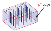
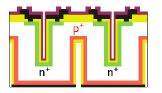
Two different types of sensors are currently under evaluation: a) full-3D sensors with active edge and electrodes penetrating through the entire wafer thickness [3] and b) partial-3D where bias and read-out electrodes do not penetrate through the entire wafer thickness and overlap by a certain amount [4] (see Figure 1). Both designs require standard VSLI processing techniques as well as Deep Reactive Ion Etching (DRIE) machining for electrode etching. In the case of the full-3D, a trench is etched, filled with p-doped polysilicon and connected to the bias electrode grid, making the edge of the sensor an electrode. The active edge considerably reduces the dead area around the sensor that is associated to planar devices.
Charge carriers drift in the silicon bulk to the read-out electrodes parallel to the wafer surface. The typical inter-electrode distance is 50-80 . The short distance between electrodes implies: a) fast charge collection, b) low full depletion voltage and c) short collection distance and consequently low charge trapping probability, and therefore high radiation hardness.
We report here beam test results on un-irradiated devices. Initial measurements on un-irradiated devices are necessary to assess the intrinsic performance of the sensors. Characterization of irradiated sensors is currently undergoing and will be reported subsequently.
2 Test Beam Instrumentation
Beam tests are crucial for performance characterization and optimization of any particle physics detector. 3D pixel sensors have been tested in beam several times in 2008 and 2009. Data presented here have been recorded in 2009 during two different periods at the CERN SPS North Area beam lines H6 (one week in October with a 120 beam) and H8 (two weeks in October/November with a 180 beam). The high momentum of the beam particles minimizes the effect of multiple scatterring which is a pre-requisite for high precision tracking measurements. Previous beam tests results have already been reported [5].
2.1 Bonn ATLAS Telescope
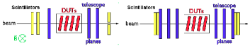
During the H8 data taking period the trajectories of the beam particles were reconstructed using the Bonn ATLAS Telescope (BAT) [6]. The telescope consisted of three double-sided silicon strip planes with a pitch in both x and y directions. Tracking resolution was estimated using a full Geant4 and telescope sensor response simulation to be [7]. Data acquisition was triggered by the coincidence of a and a scintillators located 5 meters upstream of the Devices Under Test (DUT), and a veto scintillator with a 15 mm hole located 5 meters downstream of the DUTs (see Fig. 3). The purpose of the later scintillator was to suppress showering events and to reduce the data rate.
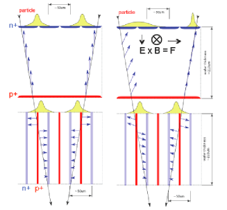
DUTs were mounted in the Morpurgo dipole magnet [8] which provided a 1.6 T vertical magnetic field at the location of the sensors. Sensors were oriented with the long pixel direction in the vertical plane in such a way that the setup reproduced the IBL ATLAS configuration.
Data were taken at several beam incident angles, ranging from to . DUTs tilt angle is described in Fig. 3. As the sensors were manually rotated, actual angles for each device were estimated from the alignment procedure.
2.2 EUDET Telescope
In the H6 setup the high resolution EUDET Pixel Telescope [9] was used for track measurement. The telescope consisted of 6 planes equally distributed into two upstream and downstream arms separated by about 40 cm. The core of the telescope is the Mimosa26 pixel sensor [10] with a pitch of . Each plane consisted of 576 x 1152 pixels covering an active area of . Triggering was achieved by the use of upstream and downstream sets of two scintillators positioned at with respect to each other. The EUDET tracking resolution has been estimated to be about .
DUTs were located between the two telescope arms and were mounted on remotely controlled rotating stages. As for the H8 beam test, a tilt angle scan was performed and data were taken at several angles varying from to . Larger angle values could not be reached due to hardware limits of the rotating stages.
A schematic of the two test beam setups is shown on Fig. 3.
2.3 Track Reconstruction
The two different telescopes require different approaches for track reconstruction.
The procedure for the Bonn ATLAS telescope consists of requiring one and only one cluster in each telescope plane. Hit positions are then estimated from these clusters, and passed to a Kalman filter [11] to obtain a fitted set of track parameters. The fitted tracks are used to align first the telescope planes, then the DUTs, using an iterative log-likelihood method. The aligned hit estimates are then passed to the Kalman filter again, and the track parameters are estimated at each DUT plane.
The Eudet telescope is read out in a rolling shutter mode [10], meaning that one trigger reads out hits in a time window of 112s. This fairly large time window increases the probability of seeing more than one track per trigger, and the amount of fake hits per trigger due to electronic noise. In this case, making a requirement of one and only one hit per plane is not viable, so a combinatorial Kalman filter [12] was implemented for track finding and fitting. Alignment was preformed using the program Millepede II. The read-out window of the DUTs is 400ns [13], so there is also a chance that a track reconstructed from the Eudet telescope planes is out of time with the DUT read-out. In the analysis of a DUT, the other DUTs in the beam are used to determine whether of not the track is in time with the DUT read-out.
There were some mechanical instabilities in the setup, making an accurate alignment hard to obtain for the full eudet data sets. For this reason data taken when the setup was most stable were selected and fitted with a deterministic annealing filter [14] for studies relying on good tracking resolution.
3 Devices Under Test
Two 3D sensors have been studied: a full-3D sensor with active edges fabricated at the Stanford NanoFabrication Facility [15] (noted as STA in the following) and a double-sided-double-type-column 3D sensor fabricated at IRST-FBK [4] (FBK) with an overlap between the n+ and p+ electrodes of . Wafer thickness was and , respectively for the STA and FBK sensors. For the sake of reference and comparison a planar sensor (PLA) of the same type as the sensors currently used in the ATLAS Pixel detector [16] was also under test.
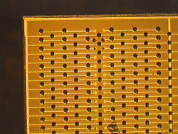
All three DUTs were bump-bonded to the ATLAS Front-End Chip I3 (FE-I3) [13]. The FE-I3 chip is an array of 160 rows 18 columns of read-out cells. It provides pixel charge measurement through digital time-over-threshold (TOT) measured in units of 25 ns, which is the LHC bunch crossing rate. Charge threshold and TOT to charge conversion have been tuned to each individual pixel to respectively 3200 e- and 60 TOT for a deposited charge of 20 ke-.
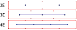
The distance between read-out and bias electrodes and therefore the number of electrodes per pixel cell is an important parameter for 3D sensors as it affects key quantities such as capacitance and noise, bias voltage, charge collection and radiation hardness. Several configurations with two (2E), three (3E) and four (4E) electrodes per cell have been studied (see Fig. 4). The optimum configuration is 3E for an FE-I3 pixel size which corresponds to an inter-electrode distance of . The 3E configuration is considered as the best trade-off in terms of capacitance and charge collection efficiency at the radiation fluence expected for the IBL.
4 Tracking Efficiency
4.1 Introduction
Tracking efficiency and resolution are fundamental features of pixel detectors. Tracking efficiency is defined as the probability of finding a hit close to a track. Previous studies have shown that 3D sensors are not efficient for normal incident tracks but recover full efficiency under a certain incident angle [17]. This is due to signal loss from tracks impinging the sensor near or in the electrodes.
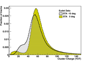
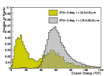
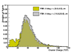
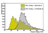
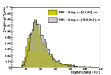
Following etching, thin layers of polysilicon and dopant (1-2 compared to electrode diameter of 15-20 and 11-12 for the STA and FBK sensors respectively) are deposited in the electrodes. In the case of the STA sensor, electrodes are subsequently filled with polysilicon [3]. Charge collection for tracks passing in the electrodes is not fully understood and it results in producing a lower response compared to tracks going through the bulk of the sensor. Given the high aspect ratio of the electrodes, track length in electrodes is small for inclined tracks, and enough charge is collected in the bulk region to fully recover efficiency. Fig. 5 shows the STA TOT distributions for normal and inclined () incident tracks from the Eudet data taking. At normal incidence the low TOT bump arises from tracks passing through the electrodes. It is attenuated for inclined tracks. FBK sensor electrodes are not filled with polysilicon and therefore have the aspect of empty holes. However, tracks are detected with high efficiency, greater than full 3D, since electrodes do not penetrate fully the sensor thickness.
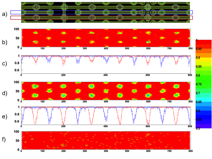
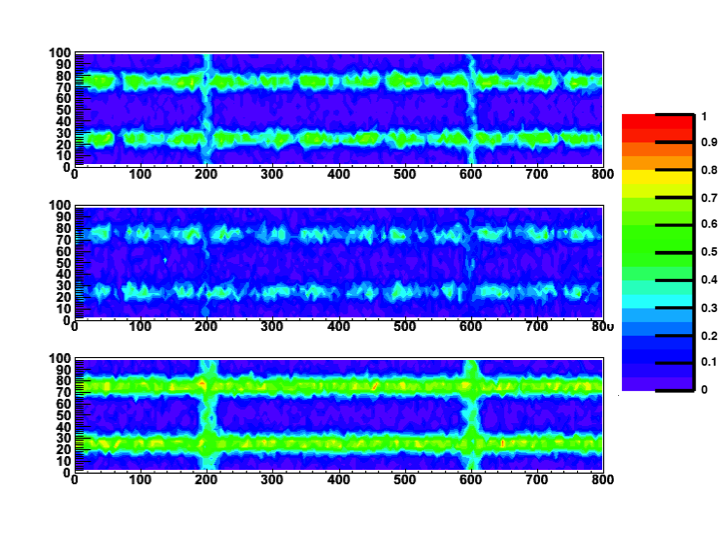
Efficiency loss in the electrodes is illustrated on Fig. 6 which shows the two-dimension efficiency maps for both the STA and FBK sensors from the Eudet data at normal incidence and at for the STA sensor. The one-dimensional projections in the read-out (blue) and bias (red) electrode regions are also shown. Electrode efficiencies are close to and for the FBK and STA sensors respectively. In the STA sensor, the tracking efficiency in the readout electrodes is slightly higher compared to bias electrodes. X-ray measurements have shown that charge collection efficiency depends on the electrode filling which is different for the two types of electrodes [18].
This same effect is clearly visible in Fig. 7: For tracks passing directly through 3D electrodes at incidence, less charge is collected, as shown by the low-ToT bump, so fewer tracks pass the charge threshold. The end result is an overall loss in efficiency. The FBK sensor is affected less strongly than the STA because its electrodes do not fully penetrate the sensor, permitting tracks at normal incidence to pass through at least part of the bulk. At tilt, tracks’ path length inside electrodes is significantly reduced, pushing the low-ToT bump to values well above threshold and fully restoring sensor efficiency. Similar performance was observed for FBK 3D sensors.
4.2 Effect of magnetic field on 3D sensors
In the ATLAS pixel detector the solenoid produces a 2T magnetic field that is orthogonal to the sensors’ electric field. Depending on the particle incident angle the Lorentz force either focusses or de-focusses the drifting charges in the sensor bulk. The minimum cluster size is achieved at the Lorentz angle value ( for the current ATLAS pixel sensors [19]). In 3D sensors however, the magnetic and electric fields are co-planar which minimizes considerably the effect of the magnetic field. Only small effects are expected. This was confirmed by our previous measurement [5]. The effect of magnetic field on planar and 3D sensors is illustrated on Fig. 8.
4.3 Efficiency as a function of tilt angle
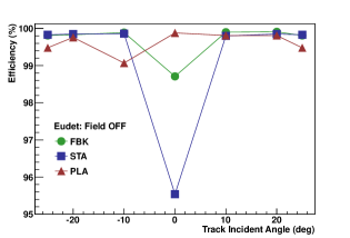
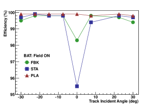
Overall efficiencies for the three devices under test have been determined as a function of the tilt angle with both the Eudet (no magnetic field) and BAT (1.6T field) telescopes.
Telescope reconstructed tracks are extrapolated to the DUTs where matching hits in space are checked for. In order to remove possible biases due to edge effects, only the central part of the sensors has been considered. Results are shown on Fig. 9. Systematic errors on the efficiencies have been estimated to from varying track selection criteria and track-hit matching requirements. Statistical errors are of the order of for the Eudet data and for the BAT data.
4.4 Charge collection as a function of tilt angle
As explained above, at normal incidence the full 3D sensor has lower efficiency, compared to the FBK sensor . However the efficiency is fully recovered () with tilt angles greater than . Consequently, both types of 3D sensors are perfectly suited to the ATLAS IBL since particle incident angles will vary from to . It is confirmed that the magnetic field has very little effect on the performances of the 3D sensors which gave similar efficiency values for field off and on.
Cluster charge has been measured as a function of the beam incident angle for both setups. Fig. 10 shows the average value of the TOT distribution of the three sensors versus tilt angle for field off and on. At zero degree beam incident angle and for the two 3D sensors, charge collection is maximum as charge sharing is minimal (see section 5). When the sensors are tilted, charge sharing increases and a fraction of the charge is lost in neighboring pixel cells that do not go over the electronics threshold. Hence, TOT decreases. At larger angles, the threshold effect is somewhat compensated by the longer path of particles in the silicon bulk which produces more charge. There is the additional effect of the Lorentz angle for the planar sensor in the magnetic field. A TOT increase near the Lorentz angle is visible.
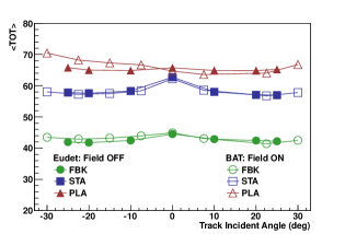
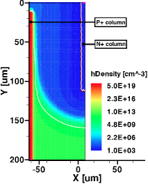
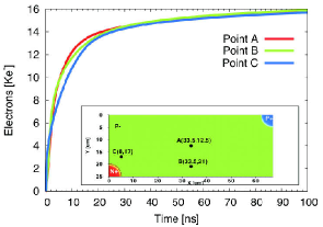
As for the FBK 3D sensor (green line with circles in Fig. 10), it should be mentioned that, due to early breakdown problems occurring at about 10 V [4], during the beam test it was biased at 8V, a voltage for which the substrate is not fully depleted. This could be confirmed by TCAD simulations. Fig. 11 shows the simulated hole density distribution along a vertical plane passing through a read-out (n+) column and a bias (p+) column: as can be seen, the region between the two electrodes is indeed depleted, but a large portion of the substrate at the bottom of the device is not depleted. As a result, charge collection is expected to be rather inefficient from the non depleted region. This is confirmed by the data in Fig. 12, showing the time integral of the simulated current pulses induced by minimum ionizing particles hitting the detector perpendicularly to the surface in three points shown in the inset, chosen as representative of different electric field conditions. The charge collected in 20 ns (peaking time of FE-I3 read-out circuit) is in the range from 13000 to 14000 electrons, in good agreement with the values indicated in Fig.10.
The STA sensor was biased at 35V and was fully depleted.
5 Charge Sharing
5.1 Introduction
Charge sharing is another important feature of pixel detector as it is directly related to tracking resolution and radiation hardness. The generated signal of a track going through a sensor can be shared between two or more cells. High charge sharing results in better tracking resolution as the track position can be more precisely determined. On the other hand, less signal will be available to each of the hit pixel cells, decreasing the probability to go above the comparator threshold and therefore being registered.
It is well known that charge collection efficiency decreases under radiation exposure. Hence it is desirable to minimize charge sharing for detectors running in a high radiation environment, such as ATLAS, in order to maintain high efficiency.
5.2 Overall charge sharing probability versus tilt angle
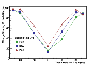
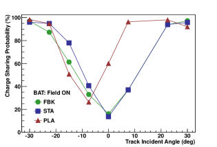
The overall charge sharing probability, defined as the ratio of the number of tracks with more than one hit over the total number of tracks , has been determined as a function of the beam incident angle for both magnetic field off and on. Systematic errors have been estimated, in a similar way as for the efficiencies, to be of the order of absolute. Results are presented on Fig. 13.
In the absence of magnetic field charge sharing is minimal at zero degree and has an expected symmetric shape versus tilt angle. Overall, charge sharing is always larger for the planar sensor compared to the 3D devices which have a similar behavior. Charge sharing is close to for absolute tilt angles larger than 20 degrees. When subject to a magnetic field, charge sharing for the planar sensor is minimum at a value corresponding to the Lorentz angle. Our fitted value is in excellent agreement with the ATLAS measurement [19] when taking into account B-field and temperature corrections.
We will note again the negligible effect of the magnetic fielf on the 3D sensors which shows similar behavior with field off and on.
5.3 Charge sharing between neighboring cells
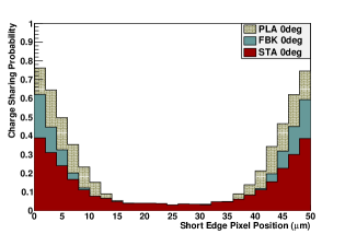
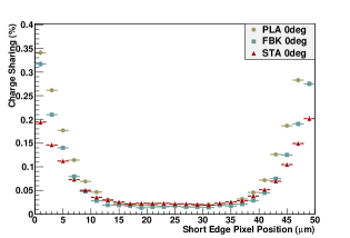
Charge sharing between neighboring cells is illustrated in Fig. 14, 16 and 16. Fig. 14 shows the two-dimensional probability of charge sharing over two neighboring cells from the Eudet data at normal incidence. Fig. 16 shows the projection on the direction of the pixel cell. As expected, charge sharing occurs predominantly in a narrow region separating two pixel cells and is clearly larger for the planar sensor to the 3D sensors. The full-3D sensor has less charge sharing compared to the FBK sensor as there is no electric field component perpendicular to the magnetic field. Charge sharing probability values do not reach 100 at the edges of the cells due to tracking resolution. Additional information is found on Fig. 16 which shows the fraction of the charge shared between two neighboring cells as a function of the hit position in the short direction.
6 Conclusion
Full and partial 3D pixel detectors have been tested, with and without a 1.6T magnetic field, in high energy pion beams at the CERN SPS North Area in 2009. Sensors characteristics have been measured as a function of the beam incident angle and compared to a regular planar pixel device. Overall full and partial 3D devices have similar behavior. Magnetic field has no sizeable effect on 3D performances. Due to electrode inefficiency 3D devices exhibit some loss of tracking efficiency for normal incident tracks but recover full efficiency with tilted tracks. As expected due to the electric field configuration 3D sensors have little charge sharing between cells.
7 Acknowledgement
We are very grateful to the ATLAS test beam coordinator Henric Wilkens, and to the EUDET, CERN SPS and North Area teams for their dedicated support and work.
References
- [1] T. Flick, Proceedings of Science (VERTEX 2009), Paper 033.
- [2] C. Da Vià et al., http://atlas-highlumi-3dsensor.web.cern.ch/atlas-highlumi-3dsensor/.
- [3] S. Parker, C. Kenney and J. Segal, Nucl. Instr. and Meth. A395, 328 (1997). C. Da Vià et al., IEEE Trans. Nucl. Sci. 56 (2009) 505.
- [4] G.F. Dalla Betta, et al., Nucl. Instr. and Meth. A, doi:10.1016/j.nima.2010.04.079.
- [5] P. Hansson et al, Nucl. Instr. and Meth. A (2010), doi:10.1016/j.nima.2010.06.321.
- [6] J. Treus et al, Nucl. Instr. and Meth. A490, 112 (2002).
-
[7]
K. Sjøbæk, thesis (2010), Oslo University.
http://www.duo.uio.no/sok/work.html?WORKID=105255. - [8] M. Morpurgo, Cryogenics, 411-414 (Jul 2009).
- [9] D. Haas, Proc. of the LCWS2007, (2007),http://www.eudet.org.
- [10] J. Baudot et al., NSS Conference Record, 2009 IEEE, 1169. 10.1109/NSSMIC.2009.5402399.
- [11] R. Früwirth, Nucl. Instr. and Meth. A262, 444 (1987).
- [12] R. Mankel, Nucl. Instr. and Meth. A395, 169 (1997).
- [13] I. Peric et al., Nucl. Instr. and Meth. A 565, 178 (2006).
- [14] R. Frühwirth and A. Strandlie, Computer Physics Communications, Volume 120, Issues 2-3, August 1999, Pages 197-214.
- [15] C. Da Vià et al., Nucl. Instr. and Meth. A 604 (2009) 505.
- [16] G. Aad (ATLAS Collaboration), JINST3, P07007, 7 (2008).
- [17] M. Mathes et al., IEEE Trans. Nucl. Sci. 55 (2008) 3731.
- [18] C. Kenney, Private communication.
- [19] P. Behera et al, ATL-COM-INDET-2010-041.