Bilayer graphene with single and multiple electrostatic barriers:
band structure and transmission
Abstract
We evaluate the electronic transmission and conductance in bilayer graphene through a finite number of potential barriers. Further, we evaluate the dispersion relation in a bilayer graphene superlattice with a periodic potential applied to both layers. As model we use the massless Dirac-Weyl equation in the continuum model. For zero bias the dispersion relation shows a finite gap for carriers with zero momentum in the direction parallel to the barriers. This is in contrast to single-layer graphene where no such gap was found. A gap also appears for a finite bias. Numerical results for the energy spectrum, conductance, and the density of states are presented and contrasted with those pertaining to single-layer graphene.
pacs:
71.10.Pm, 73.21.-b, 81.05.UwI Introduction
Low-dimensional systems have long been the subject of intensive research, both on their fundamental properties and on possible applications. In this respect the recent production of atom-thick crystal carbon layers (graphene) has raised the possibility of the development of new graphene-based devices that exploit its unusual electronic and mechanical properties (for a recent review see Ref. cast, ). The electronic spectrum of defect-free single-layer graphene is gapless and, together with the chiral aspect of the carriers in this system, leads to a perfect transmission through an arbitrarily high and wide potential barrier, i.e., the Klein paradoxklein ; kats . That can be avoided if a gap is introduced in the electronic spectrum and may be necessary for certain applications, e. g., for improving the on/off ratio in carbon-based transistors.
There are a few methods to introduce a gap in the spectrum of graphene. One of them is to use nanoribbons in which a bandgap loss arises due to the lateral confinement. Also, depositing graphene on a substrate such as boron nitride was found recently to result in a bandgapboron of meV. In bilayer graphenepartoens a gap can be introduced by applying a bias between the two layers or by doping one of them such that a potential difference results between the layers ohta ; castro ; mccann2 ; mccann . Changing the bias in the latter case can open and close the gap dynamically which is interesting for transistor applications. Nanostructured gates can thus allow the creation of quantum dots on bilayer graphene milton2 .
In this paper we investigate the electronic properties of a biased bilayer in which the potential difference between the two layers is changed periodically. Such a superlattice (SL), which can be created by applying gates to the bilayer, is of interest as it shows how a one-dimensional band structure may appear in such a system. An additional motivation is that curvature effects of corrugated single-layer graphene lead to an effective periodic potential resembling that of a SLcorrugated . Although in a bilayer this effect would be weaker, since the bilayer is less bendable than a single layer, it might still be important.
The paper is organized as follows. Section II briefly shows the basic formalism. In Sec. III results for the transmission and conductance through a finite number of barriers are presented. Section IV shows results for the dispersion relation and the density of states in SLs in bilayer graphene. Finally, a summary and concluding remarks are given in Sec. V.
II Hamiltonian, energy spectrum, and eigenstates
Bilayer graphene consists of two A-B-stacked monolayers of graphene. Each monolayer has two independent atoms A and B in its unit cell. The relevant Hamiltonian, obtained by a nearest-neighbour, tight-binding approximation near the K-point and the eigenstates read
| (1) |
Here , is the momentum operator, m/s is the Fermi velocity, and are the potentials on layers and , respectively, and describes the coupling between these layers. As shown in Appendix A, for spatially independent , , and , the spectrum consists of four bands given by
| (2) | ||||
Here , , , and . The eigenstates of are given by Eq. (32) in the Appendix.
A reduced version of the four-band Hamiltonian shown in Eq. (1) that is often usedmccann2 is given by
| (3) |
Assuming solutions of the form we can replace by . Then setting the determinant of the equation equal to zero gives rise to the two-band spectrum
| (4) |
where is the potential applied to each layer. In the next section we compare some of the results obtained from Eqs. (1) and (2) with those obtained from Eqs. (3) and (4).
III Finite number of barriers
III.1 Transmission
When applying a bias to a metallic strip a potential barrier is created; we will approximate it by a square potential barrier. The eigenstates given in Appendix A can be used in each region of constant potential. In matrix notation the wave function in region j with a constant potential can be written as a matrix product (cf. Eq. (34) of the Appendix),
| (5) |
where , , , and the superscript denotes the transpose of the row vector. Then we apply the continuity of the wave function at the different potential steps. For the potential step at we obtain
| (6) |
This links the coefficients of the wave function behind the barriers to those in front of them. Then we can write
| (7) |
where and . From now on we assume outside the barrier such that and , see the Appendix. Assuming that there is an incident wave, with wave vector from the left (normalized to unity), part of it will be reflected (coefficient r) and part of it will be transmitted (coefficient t). Also there are growing and decaying evanescent states near the barrier (coefficients and , respectively). The relation between all these waves is written in the form
| (8) |
it can be rewritten as a linear system of equations,
| (9) |
where are the coefficient of . We solved this set of equations numerically. The transmission is now given by .
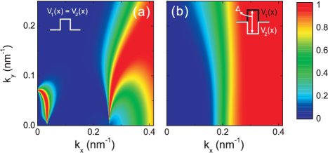
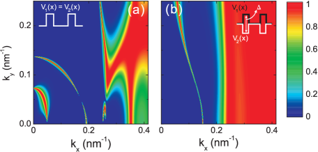
A contour plot of the transmission through a single barrier is shown in Fig. 1. Panel (a) is for a barrier with height meV and width nm and the potential difference between the layers is zero. In contrast with the case of a 2DEG, there are transmission resonances in the region which corresponds to energies lower than the barrier height. These are due to the hole states inside the barrier through which the electrons can tunnel. In panel (b) the barrier is nm wide and the potential difference between the layers is meV. As can be seen, the dependence of the transmission in panel (b) is weaker than that on and resembles more the Schrödinger case. The transmission of electrons, at normal incidence (), starts from a nm- meV which corresponds to an energy of meV which is the edge of the gap,inside which there are evanescent states which supress the transmission. For the double barrier system we see that there is also a resonance at nm-. In contrast with the single-layer case, in Fig. 1 (a) and 2 (a) there is no perfect transmission for normal incidence (), even though the system is gapless. This is a consequence of the chiral nature of the carriers in bilayer graphene (see, e.g. Ref. kats, ).
A plot of the transmission through a double barrier is shown in Fig. 2. The barriers are meV high, nm wide, and the distance between them is nm. Panel (a) is for and panel (b) for meV. In agreement with Ref. trans, we find that it is the distance L between the barriers and not their width that is important in determining the tunneling states and thus the transmission. For more results, e. g. conduction through unbiased, multiple-barrier systems see Refs. trans, and trans1, .
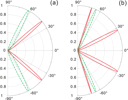
The transmission shown in Fig. 1 and 2 depends on the angle of incidence given by . A more direct way to see this is shown in Fig. 3 where the transmission is plotted as a function of the angle of incidence for constant energy meV. For panel (a) we used the Hamiltonian of Eq. (1), where a bias , while for panel (b) we used the one of Eq. (3). The differences are due to the different spectra of Eqs. (2) and (4). We consider the results of panel (a) to be more accurate than those of panel (b), since the Hamiltonian of Eq. (1) includes the effect of the non-parabolicity of the electron dispersion, which can have a strong effect on the resonant transmission of the carriers.
III.2 Conductance
It is interesting to see to what extent the transmission affects the conductance , which is given by
| (10) |
Here , is the angle of incidence measured from the axis, the transmission through the structure at energy , and the length of the structure along the direction.
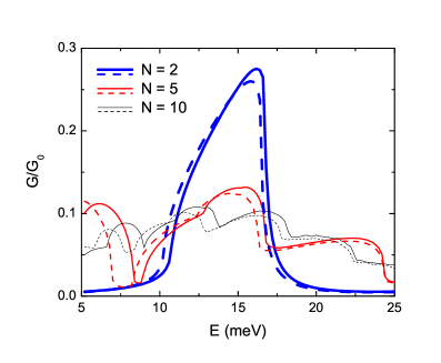
In Fig. 4 we plot the conductance through two, five, and ten barriers in blue, red, and black color, respectively. The height of the barriers is meV, their width nm, and the interbarrier distance nm. The solid curves are obtained using Eq. (1) and the dashed ones using the reduced Hamiltonian of Eq. (3) with the same coupling strength meV. As can be seen, both models give qualitatively the same results. The disagreement is mostly apparent in the low-energy region and is mainly due to the large deviation of the energy from the barrier potential , due to which the Hamiltonian approximation inside the barrier fails.
IV superlattice
IV.1 Dispersion relation
The model we used for a superlattice (SL) in graphene is shown schematically in Fig. 5. The electronic spectrum resulting from this periodic structure can be obtained by writing the solution for the spinors as Bloch waves and applying the continuity condition for the wave function at the potential steps.
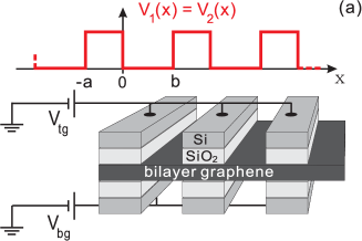
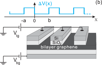
In both barriers and wells the solutions are the ones for a constant potential and the boundary conditions determine the matrix relation between the wavefunction coefficients in the two regions. For a periodic potential, Bloch’s theorem applies with period , implying . Then referring to Fig. 5 we obtain: and . Writing the wave function in the regions of constant potential as a matrix product , labelling the coefficient matrices inside the barrier regions as and the ones inside the well regions as , and applying the above boundary conditions we obtain the matrix equations
| (11) |
| (12) |
Eliminating in Eqs. (10) and (11) leads to
| (13) |
Equating the determinant of Eq. (13) to zero
| (14) |
The solution of Eq. (14) gives the energy spectrum or dispersion relation. From this determinant we search for the zeros of Eq. (14) using the Newton method and obtain the dispersion relation.
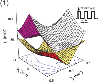
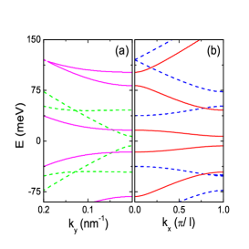

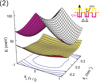
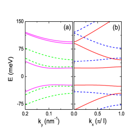
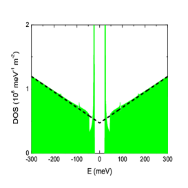
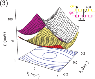
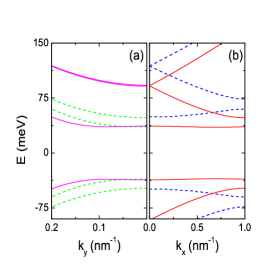

In Fig. 6 we plot the dispersion relation versus and for three different SLs. In the first one we take the potential on the back and front gates to be the same meV; between the strips the potential is meV. In the other two we only vary the bias difference between the two layers: meV in the barriers and meV in the wells for the second SL and correspondingly meV and meV for the third one. The average potential of both layers is kept constant. The parameters used are nm and the tunnel couplingohta meV. Only the first two minibands are shown in the left panels of Fig. 6. The middle column shows cross sections of the dispersion relation for constant in panels (a) and constant in panels (b).
Applying the first type of SL potential shows the formation of subbands. For this first type one can easily find an analytical expression for the one-dimensional case, i.e. , the formula for the dispersion calculated from the four-band Hamiltonian is (union of formula with and )
| (15) |
Where in region
| (16) |
The analog of this formula for the two-band approximation of the Hamiltonian is the same formula with instead of
In contrast with the gapless spectrum of SLs on single-layer graphene, here a bandgap is found for . This is in agreement with the fact that for the transmission through a barrier there is no perfect transmission for perpendicular incidence while in single-layer graphene there is. The second SL potential has the same barrier and well parameters as Fig. 2(b), the resonance at nm-1 meV which we saw in this double barrier system seems to correspond to the energy value of the first band, meV. Also, for the lowest band the mexican-hat energy profile of biased bilayer graphene is retained in the direction. In the third SL potential the gaps between the subbands are smaller than those of the second SL and the dispersion relation resembles more the (folded) one of bilayer graphene without any SL potential but with an applied constant potential difference. The DOS of the latter two SLs shows large van Hove peaks at energies corresponding to the lowest band, there also the velocity is zero and localized states form.
IV.2 Density of states
To understand part of the behavior of carriers in a SL we evaluate the density of states (DOS) . In the reduced-zone scheme it is given by
| (17) |
where is the surface area. The integral is evaluated numerically by converting it to a sum in the manner
| (18) |
where the and indices take the values
| (19) |
The cutoff for is chosen sufficiently large, we took nm-1. In addition, we replace the function in Eq. (15) by a gaussian,
| (20) |
and choose small but sufficiently large to compensate for the discretization of and , i. e. we took meV. The evaluated DOS is shown in the right panel of Fig. 6. In these figures the magenta, green and orange areas are for bilayer SLs and the red one for a single-layer SL. The dashed and dash-dotted curves show the DOS for single-layer () and bilayer () graphene in the absence of the SL potential given by
| (21) | ||||
where we used the usual tight-binding Hamiltonianlouie for single-layer graphene and the one given by Eq. (1) for bilayer graphene. The peaks in the DOS have the typical behavior of 1D subbands.
V Summary and concluding remarks
We evaluated the electronic transmission and conductance through a finite number of bilayer graphene barriers. Further, we obtained the dispersion relation and the DOS for a periodically biased bilayer, i.e., a bilayer in the presence of a SL potential. With the rapid progress in the field we expect that such a periodic biasing will soon be realized experimentally. Since the elastic mean free path of carriers in high-mobility graphene layers can be of the order of hundreds of nanometers, a ballistic behavior can be expected to be observable on the length scale of the periodic structures discussed here.
For some transmission and conductance results we used both the four-band Hamiltonian given by Eq. (1) as well as the reduced two-band Hamiltonian given by Eq. (3), cf. Fig. 4 and 5. We consider the former results as more accurate than the latter ones, since the graphene bilayer spectrum obtained from the four-band Hamiltonian is known to give a better agreement with both experimental data and theoretical tight-binding calculationsohta .
For zero bias the dispersion relation shows a finite gap for carriers with zero momentum in the direction parallel to the barriers in contrast to the well-known resultscast ; louie for single-layer graphene, cf. Fig. 6. A gap also appears for a finite bias, cf. Fig. 6. We also contrasted the DOS for bilayer graphene with the corresponding one for single-layer graphene, cf. Fig. 6. We expect that all these results will be tested experimentally in the near future.
Acknowledgements.
This work was supported by IMEC, the Flemish Science Foundation (FWO-Vl), the Belgian Science Policy (IAP), the Brazilian Council for Research (CNPq), and the Canadian NSERC Grant No. OGP0121756.VI Appendix
We assume solutions of the form . Then Eq. (1) and Schrödinger’s equation lead to the following equations
| (22a) | ||||
| (22b) | ||||
| (22c) | ||||
| (22d) | ||||
where , and . We solve Eq. (22b) for and Eq. (22d) for and substitute the results in Eqs. (22a) and (22c). This gives
| (23a) | ||||
| (23b) | ||||
For the system of Eqs. (22) and for constant potentials the spectrum is determined by the equation
| (24) |
Solving it leads to four bands ()
| (25) |
| (26) |
and four possible wave vectors
| (27) |
To obtain the general solution for the spinors we assume plane wave solutions for of the form
| (28) |
Then Eq. (22b) gives (.)
| (29) |
with replaced by , respectively, if the lower upper sign is used in and . Further, Eq. (22a) gives
| (30) |
with . Substituting in Eq. (22d) gives
| (31) |
where ; the upper signs in and correspond to the subscripts of and the lower ones to those in front of . The eigenstates are
| (32) |
is a normalization constant, such that each state carries a unit current, and is given by
| (33) |
The solution can be rewritten in the matrix form
| (34) |
with
| (35) |
and
| (36) |
The columns of the matrix product are the (unnormalized) eigenstates of our system.
References
- (1) A. H. Castro Neto, F. Guinea, N. M. R. Peres, K. S. Novoselov, and A. K. Geim, Rev. Mod. Phys. 80, (2008)
- (2) O. Klein, Z. Phys. 53, 157 (1929).
- (3) M.I. Katsnelson, K.S. Novoselov, and A.K. Geim, Nature Physics 2, 620 (2006)
- (4) B. Trauzettel, D. V. Bulaev, D. Loss, and G. Burkard, Nature Phys. 3, 192 (2007).
- (5) G. Giovannetti, P. A. Khomyakov, G. Brocks, P. J. Kelly, and J. van den Brink, Phys. Rev. B 76, 073103 (2007)
- (6) B. Partoens and F.M. Peeters Phys. Rev. B 74, 075404 (2006).
- (7) T. Ohta, A. Bostwick, T. Seyller, K. Horn, and E. Rotenberg, Science 313, 951 (2006).
- (8) Eduardo V. Castro, K. S. Novoselov, S.V. Morozov, N. M. R. Peres, J. M. B. Lopes dos Santos, Johan Nilsson, F. Guinea, A. K. Geim, and A. H. Castro Neto, Phys. Rev. Lett. 99, 216802 (2007).
- (9) E. McCann and V.I. Falko, Phys. Rev. Lett. 96, 086805 (2006).
- (10) E. McCann, Phys. Rev. B 74, 161403(R) (2006).
- (11) J.M. Pereira Jr., P. Vasilopoulos, and F.M. Peeters, Nano Lett. 7, 946 (2007).
- (12) A. Isacsson, L. M. Jonsson, J. M. Kinaret, and M. Jonson, Phys. Rev. B 77, 035423 (2008).
- (13) C. Bai and X. Zhang, Phys. Rev. B 76, 075430 (2007).
- (14) I. Snyman and C. W. J. Beenakker, Phys. Rev. B 75, 045322 (2007).
- (15) C.-H. Park, L. Yang, Y.-W. Son, M.L. Cohen, and S.G. Louie, Nature Phys. 4, 213 (2008).