Automated quantum conductance calculations using maximally-localised Wannier functions
Abstract
A robust, user-friendly, and automated method to determine quantum conductance in quasi-one-dimensional systems is presented. The scheme relies upon an initial density-functional theory calculation in a specific geometry after which the ground-state eigenfunctions are transformed to a maximally-localised Wannier function (MLWF) basis. In this basis, our novel algorithms manipulate and partition the Hamiltonian for the calculation of coherent electronic transport properties within the Landauer-Buttiker formalism. Furthermore, we describe how short-ranged Hamiltonians in the MLWF basis can be combined to build model Hamiltonians of large (10,000 atom) disordered systems without loss of accuracy. These automated algorithms have been implemented in the Wannier90 code [1], which is interfaced to a number of electronic structure codes such as Quantum-ESPRESSO, AbInit, Wien2k, SIESTA and FLEUR. We apply our methods to an Al atomic chain with a Na defect, an axially heterostructured Si/Ge nanowire and to a spin-polarised defect on a zigzag graphene nanoribbon.
keywords:
Electronic structure , density-functional theory , transport , Wannier function , Wannier90PACS:
73.63.-b , 72.10.-d , 71.15.Ap1 Introduction
Nanostructured materials, such as carbon nanotubes and silicon nanowires, promise advances in wide-ranging device applications such as photonics[2], thermoelectrics [3, 4] and biological/chemical sensing[5]. Successful incorporation of such structures in real devices requires bottom-up approaches to design, which in turn, require an understanding of electronic transport at the nano and mesoscales.
First-principles simulations based on density-functional theory (DFT) are now well-established as a powerful tool for materials modelling. Their success is largely due to the high accuracy and computational efficiency that can be obtained for many classes of materials.
Notwithstanding concerns regarding its ability to describe charge transport in certain situations [6], DFT combined with the Landauer formulation [7] has become a standard starting point for evaluating quantum conductance (QC) [8, 9, 10, 11, 12, 13, 14, 15, 16, 17]. Calculations typically adopt a ‘lead-conductor-lead’ geometry (Fig. 1 (top)) whereby the conductor is sandwiched between two contacts, or leads, whose semi-infinite nature is accounted for by means of surface Green’s functions and self-energies [18] obtained from standard DFT calculations.
Despite the success of this approach, realistic nanoscale systems, which typically contain arbitrary distributions of impurities, functionalizations and modulations of structure and composition are challenging to describe accurately due to the asymptotic cubic scaling of conventional DFT calculations with respect to system size.
In this Article, following Lee et al. [14] and Cantele et al. [19], we use a method based on the transferability of maximally-localised Wannier functions (MLWFs) [20, 21] in order to overcome the cubic-scaling bottleneck. The novelty of our work lies in the development of robust algorithms for the complete automation of the often painstaking manipulations required for preparing a Hamiltonian matrix in the MLWF basis. As a result, high-throughput computations of QC requiring little user intervention become feasible for disordered nanoscale systems. Two further important features of our method are (i) that the MLWF basis is optimally compact, ensuring highly efficient determination of QC and density of states (DoS), and (ii) that the nearsightedness of the electronic interactions can be exploited in the MLWF basis by piecing together, without loss of accuracy, Hamiltonians from DFT calculations on small fragments to form model Hamiltonians of complex nanostructures consisting of tens of thousands of atoms or more.
The remainder of this paper is structured as follows: Sec. 2 describes briefly the underlying theory of Landauer transport and MLWFs, the real-space basis in which the transport calculations are performed; Sec. 3 describes the details of the implementation of our automated method within the Wannier90 code [1]; in Sec. 4 we present the results of our approach on a number of systems; finally, Sec. 5 is reserved for our concluding remarks.

2 Theoretical Background
2.1 Landauer Transport
Within the Landauer formalism, it is assumed that there are no dissipative scattering events on the length scale of the conductor region, such that transmission is coherent, or ballistic. For a single conducting channel at each energy , Landauer showed [7] that the zero-bias, zero-temperature conductance is given by
| (1) |
where is the probability of transmission through the conducting channel. In this framework, is called the quantum conductance (QC). Extending this formalism to multiple channels [22, 23, 24] one may write
| (2) |
where are the retarded (r) and advanced (a) Green’s functions associated with the conductor, and are functions that describe the coupling of the conductor to the left (L) and right (R) leads.
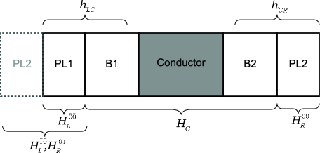
The standard approach used to determine the QC of nanostructures that has emerged in recent years employs a localised basis set so that the Hamiltonian of a system in the lead-conductor-lead geometry (Fig. 1 (top)) may be partitioned unambiguously. A principal layer [25, 26] (PL) is introduced, which is long enough so that if , where is the basis function in the PL and is the Hamiltonian operator for the entire system. By imposing the equality on the Hamiltonian elements, a truncation error is introduced, which is controlled systematically by increasing the size of the PL (as will be shown in Sec. 4). The Hamiltonian matrix, with reference to the bottom panel of Fig. 1, then takes tri-block diagonal form,
| (3) |
where interactions between the first PL of the left or right lead and the conductor are and , respectively; and are matrices formed by orbitals in the same PL in the semi-infinite left and right leads, respectively, and and are matrices formed by orbitals in adjacent PLs in the left and right leads, respectively. As shown in Eq. (3), these latter four matrices are periodically repeated to form and (defined in the bottom panel of Fig. 1).
2.2 Green’s Function Formalism
Knowledge of the seven finite Hamiltonian sub-matrices , , , , and is sufficient to describe the open system of Fig. 1 and to calculate the QC from Eq. (2). Following Nardelli [27], in order to determine and , we first consider the Green’s function of the whole system,
| (4) |
where () for . Since , in the following we focus on only and suppress the superscript. From Eq. (4) it can be shown that [18]
| (5) |
where and represent self-energy terms due to the coupling of the conductor to the leads. are known as surface Green’s functions and can be computed efficiently via the iterative procedure of Lopez-Sancho et al. [28]. is related to the local density of states (DoS) of the conductor by [18]
| (6) |
Finally, the coupling functions are given by [18]
| (7) |
In the special case that the lead and conductor are identical and the entire lead-conductor-lead system is translationally invariant, the following simplifications can be made: , and . Such systems are hereafter referred to as bulk, or pristine, systems and transport calculations thereupon are referred to as bulk, or pristine, transport calculations. In our results, we will compare the QC of disordered conductors with the corresponding bulk, or pristine, QC.
2.3 MLWF Basis
In a periodic crystal, within the independent particle approximation, electrons are described by bands, or Bloch states with band index and crystal momentum . An entirely equivalent representation may be constructed in terms of Wannier functions , obtained by Fourier transforming in the pair of conjugate variables and , where labels the lattice vector of the real-space cell in which the Wannier function is centered. Unlike Bloch functions, however, Wannier functions may be constructed that are localized in real space, exhibiting exponential decay in systems with an electronic band-gap [29]. Even in a metal, exponential localisation can be achieved if an appropriate combination of filled and empty states is used[14].
For an isolated band, observables are invariant under a gauge transformation of the form . Different choices of the phase , however, will result in different Wannier functions, and can therefore be used as a means of making the resulting Wannier function as localised as possible. Marzari and Vanderbilt [20] showed that for a composite, yet isolated group of bands (such as those found in the valence manifold of an insulator of semiconductor), one may define a set of generalised Wannier functions
| (8) |
where is a unitary matrix that may be chosen such that the Wannier functions are maximally-localised i.e. that the sum of their quadratic spreads
| (9) |
where and , takes the smallest value possible.
When a set of bands is not isolated from the rest of the band structure by a gap across the Brillouin zone, the bands are said to be connected or entangled. This is the case in metals and in conduction manifolds of semiconductors and insulators. In such cases, within a given energy window, the number of bands at each point in k-space varies and the disentanglement procedure of Souza et al. [21] is used in order to extract, or disentangle, an optimally-connected subspace of a given, constant dimension at each . Once this optimal subspace has been obtained, the usual localization procedure of Marzari and Vanderbilt [20] may be applied in order to determine the MLWFs. Once obtained, these provide a real-space and often intuitive picture of bonding in materials, to the point that they are now used widely as a post-processing tool in electronic structure calculations [1].
There are a number of advantages to using MLWFs. First, they span a much smaller subspace compared to, say, the plane-wave basis in which the original ground-state electronic structure calculation is performed. The space of MLWFs is arguably the most compact, minimal manifold possible (1 MLWF per every band that needs to be described), while still preserving in full the accuracy of the electronic structure calculation. As a result, matrices in an MLWF basis can be orders of magnitude smaller in each dimension than in the original basis, while still reproducing exactly the properties of the ground-state, thus enabling very efficient and accurate computation of ground-state properties, such as interpolated band structures [30]. For example, the band structure of the valence manifold for silicon is equivalently described by 3000 plane-waves per atom or 2 MLWFs per atom. Second, since they are localised in real-space, MLWFs may be used to represent the Hamiltonian of a system in sparse matrix form. Finally, this sparsity may be exploited in order to build model Hamiltonians of large, structurally complex systems from Hamiltonians of smaller fragments.
3 The Single Supercell Geometry
The translational symmetry present in crystals is exploited in electronic structure calculations by using supercells and periodic boundary conditions (PBC). A natural basis set to use for such calculations is that of plane-waves and their benefits for DFT calculations are well-understood [31].
The lead-conductor-lead geometry of Fig. 1, however, is inherently non-periodic. Therefore, as outlined in Sec. 2, if we are to use PBC for our Landauer conductance calculations, a transformation to a localised basis set, such as MLWFs, becomes essential.
Furthermore, the vast range of structural combinations that one could investigate means that the change of basis must be coupled to a robust and user-friendly algorithm that automatically prepares the Hamiltonian obtained from a calculation on a periodic system for use in the transport calculation so that high-throughput calculations are possible. The novelty of our work lies in the automation of these non-trivial manipulations of Hamiltonian matrices and in streamlining the calculations such that a calculation on only a single supercell is required; we call this the Single Supercell Geometry (SSG).
The SSG is shown in Fig. 2, whereby a central conductor is sandwiched between a length of lead on the left and right. The conductor is the disordered region under investigation and the leads are the contacts whose bulk is periodically repeated ad infinitum in the open (lead-conductor-lead) system. We split each lead into two parts: the outermost regions must be a PL of lead (PL1 and PL2) and the inner regions a buffer (B1 and B2) such that any disorder within the electronic structure associated with the conductor is localised within the region marked . In this respect it is important to converge results with respect to the size of the buffer regions; we also impose that B1 and B2 must be at least one PL of lead in length.
By transforming to a MLWF basis, our algorithm uses the SSG to identify the Hamiltonian sub-matrices required for the transport calculation. Fig. 2 depicts these regions. For the sake of clarity, it is worth highlighting first that is in fact built from the contribution of MLWFs within the conductor and the buffers, and second that the interaction between two adjacent PLs of lead, and , are built from Hamiltonian matrix elements between MLWFs in PL1 and the periodic image of PL2. For this reason, we demand that the left and right leads of the SSG be identical in nature.
The Hamiltonian sub-matrices attained from partitioning the total Hamiltonian require a number of operations performed on them before they can be input into transport calculations. First, we need to re-order the MLWFs in real-space so that every unit cell in PL1, PL2, B1 and B2 has a consistent sequence of MLWFs. This is because the Hamiltonian corresponding to the semi-infinite leads is constructed from sub-matrices extracted from the SSG Hamiltonian in the MLWF basis. The connection matrix is constructed from the Hamiltonian matrix elements between MLWFs in PL1 and the periodic image of PL2, whereas is constructed from PL1 only. These two matrices are then duplicated along the block off-diagonal and block diagonal, respectively, of the Hamiltonian of Eq. (3). In doing so, the implicit assumption is that the sequence of MLWFs in the rows and columns of the Hamiltonian sub-blocks are the same, which in general is not true. To overcome this problem we use the positions of the MLWF centres in real-space to order the elements of the Hamiltonian sub-matrices: the MLWFs in each unit cell of lead are arranged first according to their position along one direction perpendicular to the transport direction, then in the other perpendicular direction, and finally along the transport direction itself. This ensures that the sub-matrices can be used consistently to build the Hamiltonian of Eq. (3).
The shape of MLWFs are often chemically intuitive and display atomic-like or bonding/anti-bonding orbitals. Thus if more than one MLWF exists with precisely the same centre, as may happen with -like MLWFs on a transition metal site, a second level of ordering based on the orbital character of the MLWF is performed, employing a technique we have developed using spatially-dependent integrals to deduce a unique signature for each MLWF (see A).
In addition to the ordering of the MLWFs, a second consistency criterion must also be imposed. The issue stems from the fact that, although MLWFs are always found to be real, they remain undetermined upto an overall sign, or parity. As with the issue of ordering the MLWFs, the procedure of building the Hamiltonian from sub-matrices implicitly assumes that the MLWFs in PL2 have the same parity pattern as those in PL1, which in general is not true.
To address this issue, we enforce a consistent parity pattern at the level of the unit cell of lead onto the ordered Hamiltonian sub-matrices (PL1, B1, B2 and PL2). The parities of the MLWFs in the leftmost unit cell of lead in the SSG supercell are used as the template. By assessing the relative parity of MLWFs in this unit cell compared to translationally equivalent MLWFs in the other unit cells of the PLs and buffer regions, the pattern is enforced throughout by multiplying by , as appropriate. The relative parities are determined by using the unique signature associated with each MLWF.
We outline three caveats that apply to the current implementation of the SSG method: (i) the Bloch states used as input for determining the MLWF basis in the SSG are calculated at the -point only; (ii) the lattice vectors of the SSG must form a orthorhombic set and the direction of conduction must be in the , or direction. (iii) the system under investigation must be quasi-one-dimensional (although the extension to bulk leads would be relatively simple to implement.)
3.1 Calculation Procedure
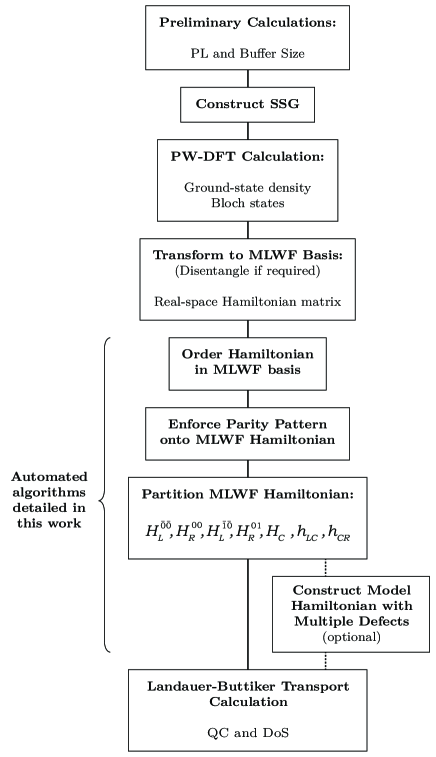
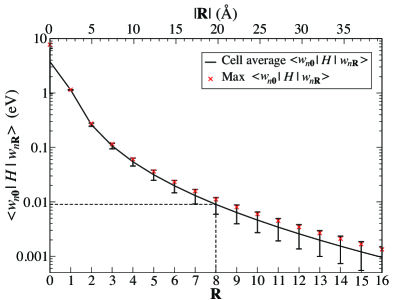
We now outline our general method, this is shown schematically in Fig. 3. First we must determine the number of unit cells that make up a PL. Consider a supercell of lead with unit cells along the conduction direction, whose Hamiltonian in the MLWF basis is found from a -point DFT calculation in PBC. The value of is chosen such that Hamiltonian matrix elements between MLWFs in the central unit cell and the left-most unit cell are less than a certain threshold, which is usually set to be around 10 meV. In practice, for computational efficiency, instead of a -point supercell calculation, we apply Bloch’s theorem to reduce the supercell to a single unit cell, and perform the DFT calculation on a regular grid of k-points in the conduction direction. This calculation is also used to calculate the bulk, or pristine, QC which is used for validation purposes (see Sec. 4).

Next, the extent of the buffer is determined by assessing the convergence of electronic structure in PL1 and PL2 with respect to its size. If the disorder present in the conductor region is short-ranged, then often a single PL of lead in B1 and B2 is sufficient. This point is illustrated in Fig. 4: we see that beyond a few unit cells from a defect (hydrogen functionalization in a (3,3) carbon nanotube), the on-site Hamiltonian matrix elements of the MLWFs recover their bulk value. Once the extent of the buffer and PLs have been determined, the SSG supercell may be built and its Bloch eigenstates found from a conventional DFT calculation. This calculation is usually performed in two steps. First, a self-consistent calculation at enough k-points to converge the charge density, followed by a non-self-consistent calculation at the -point only, using the self-consistent charge density as an input.
Transformation to the MLWF basis, Hamiltonian-matrix preparation, and transport calculations may then be performed. The automated algorithms described above, which are implemented in the Wannier90 [1] code are designed so these steps are performed sequentially, with little or no intermediary user input. A natural validation of the results may be performed whereby the disordered conductor region of the SSG is replaced by a section of pristine lead: identical results should be achieved with the bulk calculation.
3.2 Combination of multiple defects
Moving from a Bloch to a Wannier representation is not only a means by which to represent electronic structure in a very compact manner. It also opens the possibility to exploit the real-space nature of the basis to build very large systems – systems so large that a conventional DFT calculation would be intractable.
The fact that electronic nearsightedness becomes explicitly manifest in the MLWF basis, as highlighted in Fig. 4, allows them to be used to build the Hamiltonian matrix of a large structure from the smaller Hamiltonian matrices of its constitutive sub-systems.
In order to illustrate the method, consider the schematic lead-conductor-lead system shown in Fig. 5 in which the conductor region has two identical defects separated by a region of lead material in the form of a buffer (B1′ and B2′). We could calculate the QC of this structure by making a SSG with the whole conductor (regions and ). However, we may exploit the nearsightedness of the MLWF basis to find a more computationally efficient approach. If the effect of the defects is localised (in the sense that the local electronic structure and geometry at the junction between B1′ and B2′ is sufficiently similar to that seen in the leads), then we may construct the Hamiltonian for the system with two defects (Fig. 5) from information gathered from one SSG calculation containing just a single defect (Fig. 6). Since this system is smaller, there is a clear advantage in terms of computational cost for the initial DFT calculation.


The Hamiltonian of the conductor in the two-defect system may be written as
| (10) |
where , and represent blocks of Hamiltonian matrix elements among MLWFs in region , among MLWFs in region , and between MLWFs in these two regions, respectively.
Given the geometry of the system, and the nearsightness of the electronic structure, blocks and should be quite close in terms of their matrix elements. Moreover, because of the constraint that a buffer is at least as large as a lead principal layer, we expect the non-zero matrix elements of to correspond closely to the overlaps between the two adjacent principal layers. This observation stems from the very definition of a principal layer. As a consequence, we can construct a close approximation to by using the matrices extracted from a SSG calculation of the structure shown in Fig. 6. In this approximation, blocks and are replaced with , and is replaced by the overlap matrix between two principal layers of lead (namely , see Fig. 2), i.e.,
| (11) |
An example of this approach is demonstrated in Sec. 4 for a defected silicon nanowire.
The approach described above is general and may be applied to any number of isolated defects in the conductor region. In this way, Hamiltonians for systems of almost arbitrary size may be constructed with first-principles accuracy from one DFT calculation in a SSG with a single defect. We note in passing the importance that the MLWFs parities are consistent between different regions of the system. As mentioned in Sec. 3, the parities need to be checked and made consistent to allow seamless connections between Hamiltonian sub-matrices, a task that is automatic in the present approach.
Furthermore, the Hamiltonian of a conductor with more than one type of defect may be constructed by combining matrix elements from separate SSG calculations. In this latter case, care must be taken in order to align the Fermi energies of the two (or more) distinct calculations. This is the consequence of the lack of an absolute reference for the electrostatics in PBCs, which can lead to Fermi energies that are shifted by a constant.
Additionally, building a large-scale structure with tens of defects and tens of thousands of atoms can be a painstaking task. In order to simplify this process, we have designed a utility package to the Wannier90 code that helps the user create these large scale structures. From a single Wannier90 calculation in the SSG geometry, both randomised and custom-made structures can be built with ease. An illustration of the use of that functionality is given in the fourth example of Sec. 4.
4 Applications
We present now a number of examples using the method described in Sec. 2. The aim is to illustrate its robustness in a range of applications: beginning with a defected atomic chain, and building complexity via a heterostructured nanowire and a spin-polarised graphene nanoribbon. Finally, we provide an example to validate the use of SSG Hamiltonian fragments in the construction of model Hamiltonians for larger systems. All DFT calculations are performed with the Quantum-ESPRESSO package[32] and with (unless otherwise stated) norm-conserving pseudopotentials.[33]
4.1 Atomic Al Chain
First, we consider the QC of an Al chain with a single Na atom substitutional defect. The construction of the SSG is performed with care: a suitable PL length must first be decided upon by assessing the rate of the decay of the matrix elements of the Hamiltonian between MLWFs. Additionally, the defect is expected to have a large effect on the electronic structure, thus the buffer size must also be carefully chosen.
To assess the length of a PL we use the method outlined in the Sec. 3.1, whereby the Hamiltonian in the MLWF basis of a single unit cell of lead is determined at many k-points. We perform the DFT calculation on a single unit cell (consisting of one Al atom), with a regular grid of 32 k-points along the extended direction. The total energy is converged to eV using a 500 eV energy cut-off, exchange and correlation are described by the PBE functional[34]. The unit cell is 2.47 Å long in the conduction direction, with 10 Å separating periodic images in the transverse directions. We proceed to the determination of the MLWF basis by disentangling three Wannier functions from 30 bands.
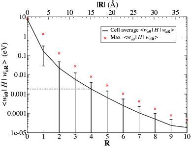
Fig. 7 shows the decay of the interaction between MLWFs by averaging the on-site Hamiltonian elements between equivalent MLWFs in different unit cells labelled by the primitive lattice vector (black solid line). The maximum matrix element (red crosses) gives the maximum error incurred due to truncation of the interaction if the PL were to be cut at that unit cell. In this case, the PL is chosen to be eight unit cells long, such that the maximum truncation error is approximately 11 meV and the average error is 9 meV.
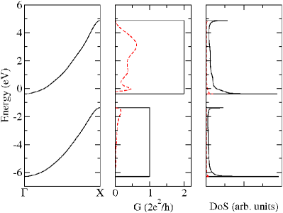
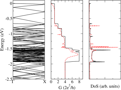
A buffer size of one PL plus three unit cells is chosen for the SSG such that on relaxation the RMS difference in the position of the MLWF centres from their ideal bulk position in the rightmost unit cell of PL1 is less than Å. The SSG therefore consists of a total of 39 atoms. Performing the transport calculation provides the QC and DoS shown in Fig. 8 (red, dashed; centre and right panels, respectively). For comparison, the bulk band structure, QC and DoS (black; left, centre and right panels, respectively) are also shown. In the bulk case there are clear contributions from the band and two degenerate bands to the QC: these are both significantly reduced in the defected case, with conductance close to zero at lower energies. This may be interpreted as the hybridization of the orbital associated with the Na to adjacent Al orbitals.
4.2 Si/Ge Nanowire Heterostructures
We now increase the complexity of the SSG system by considering a thin (0.39 nm radius) Si nanowire in the direction with a Ge heterostructure inserted as a defect. The DFT calculations detailed in this example (and those on the nanowires of in Sec. 4.4) are performed within the LDA and with an energy cutoff of 400 eV. We begin with a single cell for the lead (8 Si atoms, 8 H atoms) (see Fig. 9 (top)) and perform a DFT calculation with 20 k-points, allowing atomic positions and lattice parameter in the conduction direction to relax. Forces are converged to 5 meV/Å. Once the ground-state is found, we transform to the MLWF basis and assess the PL length in the usual manner. Fig. 10 displays the decay of the Hamiltonian matrix elements as a function of increasingly distance, using the same notation as Fig. 7. With four unit cells in a PL the average truncation error is below 2 meV.
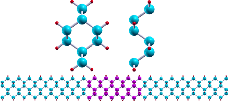
A SSG is built by repeating the single unit cell of Si and inserting 5 copies of a similarly relaxed Ge unit cell (see Fig. 9, bottom panel). Without further relaxations of the geometry, it was found that a single PL was sufficient to converge the electronic structure in PL1 and PL2 to that of a bulk lead. Hence our SSG consisted of 16 Si unit cells with five Ge unit cells sandwiched at their centre (Fig. 9, bottom panel). Using our automated routines, this 336 atom unit cell provides the valence QC and DoS shown in Fig. 11 (red, dashed lines; centre and right panels, respectively). The bandstructure, QC and DoS of the pristine silicon nanowire are also shown (black solid lines; left, centre and right panels, respectively). The drop-off in conductance just below the Fermi level is due to localization of the highest occupied molecular orbital within the Ge quantum well.
4.3 Spin-polarised graphene nanoribbon
In this third example, we look at a spin-polarised graphene nanoribbon functionalised with a single hydrogen atom. As with the previous examples, we start with a calculation on a single unit cell. Our system is a zigzag nanoribbon of length 2.46 Å with a width of 9.27 Å. A regular grid of 20 k-points is used in the conduction direction and the supercell is built such that a vacuum region of 10 Å lies between periodic images. A cutoff of 400 eV for the kinetic energy and 4500 eV for the charge density is used together with a PBE exchange and correlation functional and ultrasoft pseudopotentials[35]. Both the atomic positions and the unit cell length were fully relaxed; individual forces are less than 18 meV/Å.
We must specify a starting non-zero magnetization such that the self-consistent loop converges to a magnetic state (in this case we restrict ourselves to a ferromagnetic state, even though the ground state is anti-ferromagnetic [36]). Next, a non-self consistent calculation is used to compute the band energies for both “up” and “down” spins. It is important at this stage to compute a sufficient number of bands to capture the entire manifold, otherwise the disentanglement of the conduction manifold would be meaningless. In our calculations, we used 30 bands and we kept all the bands up to eV in the frozen window for the disentanglement procedure.
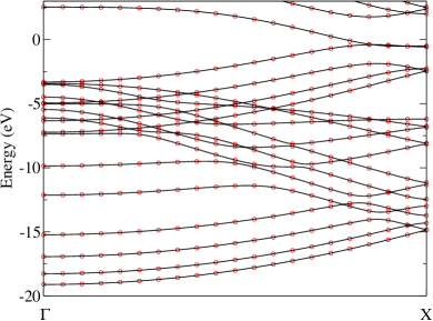
The quality of the disentanglement may be assessed by comparing the interpolated band structure provided by Wannier90 to the full band structure given by the electronic structure code (for this ferromagnetic state, both spin types have an almost identical band structure except around the Fermi level). As can be seen from Fig. 12, the match between the Wannier interpolation (solid lines) and the “true” band structure (dots) is excellent. We see that the interpolated band structure describes perfectly conduction states upto about 2.5 eV above the Fermi energy.
Satisfied with the MLWF transformation, the PL size is assessed in the manner described earlier. Choosing a PL size of four unit cells (with a maximum truncation error of less than 46 meV) is sufficient for this example.
The SSG consists of 4 unit cells of lead in both the PL1, PL2, B1 and B2 regions. Two unit cells form the conductor region (see Fig. 13), upon which a hydrogen atom is placed at an approximate C-H bond length above one of the carbon atoms. The whole system is fully relaxed both for atomic positions and supercell length in the direction of conduction. The force convergence criteria, cutoffs and energy convergence criteria are similar to the ones used in the single lead unit cell case above.
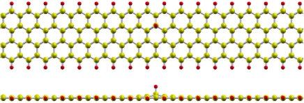
After relaxing the structure, the next step is to perform a spin-polarised DFT calculation followed by a non-self consistent calculation to extract the “up” and “down” band energies at . The QC is calculated in the usual manner for each spin channel separately with Wannier90. The result for the spin-dependent QC is shown in Fig. 14.
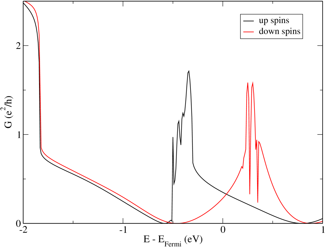
We see on the graph that at the Fermi level the quantum conductance of the system is slightly spin-polarised with a majority of “up” spins. Applying a slightly negative bias, we see that the system can be close to 100 spin-polarised. The opposite spin polarization can be achieved with a slightly positive bias.
4.4 Doubly Defected Si Nanowire
This final example demonstrates an extension to the SSG method whereby the sub-Hamiltonians it creates are manipulated and combined to construct model Hamiltonians of larger systems (see Sec. 3.2). All DFT calculations outlined here are performed within the LDA, at the point, with the same energy cut off and tolerances described in Sec. 4.2.
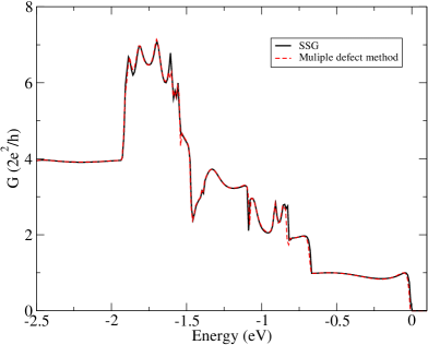
The system we aim to describe is shown in Fig. 15 (top): a Si nanowire with two single cells of Ge separated by a length of Si. This system may be thought of in two ways: first, as a Si nanowire with a single defect containing the two cells of Ge and the separating Si cells; and second as doubly defected Si nanowire, with each defect being a single cell of Ge. These two perspectives lead to two methods by which we can determine the QC. The first suggests a SSG calculation in which the conductor region contains the two Ge defects. The resulting QC is see in solid black in Fig. 15 (bottom). This is compared to the QC derived from a calculation in which the multiple defect method described in Sec. 3.2 is used.
For the doubly defected case, we perform a SSG calculation on a Si nanowire with a single Ge cell defect and use the Hamiltonians provided to build a Hamiltonian of the larger system in question (Fig. 15 (top)). The QC from this calculation is seen in dashed red in Fig. 15 (bottom). The two calculations agree remarkably well, validating the premise of nearsightedness discussed earlier. Since the computational expense of conventional DFT methods scales as , where is the number of atoms in the supercell, the multiple defect method represents a significant step forward to describe realistic system sizes with first-principles accuracy, and can be used to construct faithful model Hamiltonians for systems that contain tens of thousands of atoms[37, 38].

5 Conclusions
In this paper we have presented a user-friendly and automated approach to calculate the quantum conductance and density of states in quasi-one-dimensional systems. The method converts the Bloch eigenstates of a single DFT calculation, within our single supercell geometry, to a basis of MLWFs. In this basis we determine the electronic transport properties by automatically extracting the Hamiltonian sub-matrices required for the transport calculation. To illustrate the robustness, wide applicability and efficiency of our method, we have presented calculations on an atomic Al wire, a spin-polarised graphene nanoribbon, and axially heterostructured Si/Ge nanowires. Furthermore, we have shown how the transport properties of meso-scale conductors that are beyond the current capabilities of conventional first-principles electronic structure calculations can be calculated with first-principles accuracy by exploiting the transferability of MLWFs as building blocks of large model Hamiltonians.
Acknowledgements
We would like to thank the Imperial College High Performance Computing Service for continued use of their facilities and the developers of the Quantum-ESPRESSO package [32]. We are also grateful to Davide Ceresoli and Young-Su Lee for their advice and help. Financial support was provided by Research Councils UK, the UK Engineering and Physical Sciences Research Council, The Institute for Soldier Nanotechnology at MIT and the Thomas Young Centre for Theory and Simulation of Materials.
Appendix A MLWF Signatures
Here we detail the set of spatially-dependent integrals that we use to determine a signature for each MLWF. These signatures are used for two purposes. First, they enable a sorting algorithm to distinguish between MLWFs of different shapes with similar centers. Thus they may be ordered consistently over between unit cells – a key requirement for our approach. Secondly, they are used to determine the relative parity of MLWFs so that a consistent parity-pattern may also be enforced.
We begin with the integral
| (12) |
where is the volume of the cell, is a vector in reciprocal space and is the centre of Wannier function (we assume sampling at -point only). One may write , where is the periodic part of the Bloch wavefunction at band . is the unitary matrix found in Eq. (8) that minimises the spread of the Wannier functions. can be written in terms of its discrete Fourier transform , . Thus, the integral in Eq. (12) may be written as
| (13) |
where is a -vector of the form , where and are the reciprocal lattice vectors. Equating real and imaginary parts of Eq. (12) and Eq. (13), one may write
| (14) |
and
| (15) |
Since most DFT codes compute , obtaining any set of incurs negligible computational expense.
The set of integrals that are used to determine a signature are given by
| (16) |
where , , and . Each of the resulting 20 integrals may be written as linear combinations of those outlined in Eqs. (14) and (15). The signature of the MLWF is thus given by the 20-element unit vector of these integrals. Dot products between two MLWFs’ signatures reveal in a compact form their relative shape and parity.
References
- Mostofi et al. [2008] A. A. Mostofi, J. R. Yates, Y.-S. Lee, I. Souza, D. Vanderbilt, N. Marzari, wannier90: A tool for obtaining maximally-localised Wannier functions, Computer Physics Communications 178 (2008) 685.
- Cui et al. [2001] Y. Cui, Q. Wei, H. Park, C. M. Lieber, Nanowire nanosensors for highly sensitive and selective detection of biological and chemical species, Science 293 (2001) 1289–1292.
- Hochbaum et al. [2008] A. I. Hochbaum, R. Chen, R. D. Delgado, W. Liang, E. C. Garnett, M. Najarian, A. Majumdar, P. Yang, Enhanced thermoelectric performance of rough silicon nanowires, Nature 451 (2008) 163.
- Boukai et al. [2008] A. I. Boukai, Y. Bunimovich, J. Tahir-Kheli, J.-K. Yu, W. A. G. III, J. R. Heath, Silicon nanowires as efficient thermoelectric materials, Nature 451 (2008) 168.
- Atwater and Polman [2010] H. A. Atwater, A. Polman, Plasmonics for improved photovoltaic devices, Nat Mater 9 (2010) 205–213.
- Koentopp et al. [2008] M. Koentopp, C. Chang, K. Burke, R. Car, Density functional calculations of nanoscale conductance, J. Phys.: Condens. Matt 20 (2008) 083203.
- Landauer [1970] R. Landauer, Electrical resistance of disorder one-dimension lattices, Phil. Mag. 21 (1970) 853.
- Nardelli et al. [2001] M. B. Nardelli, J. L. Fattebert, J. Bernholc, O(n) real-space method for ab initio quantum transport calculations: Application to carbon nanotube-metal contacts, Phys. Rev. B 64 (2001) 245423.
- Taylor et al. [2001] J. Taylor, H. Guo, J. Wang, Ab initio modeling of quantum transport properties of molecular electronic devices, Phys. Rev. B 63 (2001) 245407.
- Brandbyge et al. [2002] M. Brandbyge, J. L. Mozos, P. Ordejon, J. Taylor, K. Stokbro, Density-functional method for nonequilibrium electron transport, Phys. Rev. B 65 (2002) 165401.
- Wortmann et al. [2002] D. Wortmann, H. Ishida, S. Blügel, Embedded Green-function approach to the ballistic electron transport through an interface, Phys. Rev. B 66 (2002) 075113.
- Thygesen et al. [2003] K. S. Thygesen, M. V. Bollinger, K. W. Jacobsen, Conductance calculations with a wavelet basis set, Phys. Rev. B 67 (2003) 115404.
- Calzolari et al. [2004] A. Calzolari, N. Marzari, I. Souza, M. B. Nardelli, Ab initio transport properties of nanostructures from maximally localized Wannier functions, Phys. Rev. B 69 (2004) 035108.
- Lee et al. [2005] Y. S. Lee, M. B. Nardelli, N. Marzari, Band structure and quantum conductance of nanostructures from maximally localized Wannier functions: The case of functionalized carbon nanotubes, Phys. Rev. Lett. 95 (2005) 076804.
- Thygesen and Jacobsen [2005] K. S. Thygesen, K. W. Jacobsen, Molecular transport calculations with Wannier functions, Chem. Phys. 319 (2005) 111–125.
- Polizzi and Ben Abdallah [2005] E. Polizzi, N. Ben Abdallah, Subband decomposition approach for the simulation of quantum electron transport in nanostructures, J. Comp. Phys. 202 (2005) 150–180.
- Havu et al. [2006] P. Havu, V. Havu, M. J. Puska, M. H. Hakala, A. S. Foster, R. M. Nieminen, Finite-element implementation for electron transport in nanostructures, J. Chem. Phys. 124 (2006) 054707.
- Datta [1995] S. Datta, Electronic Transport in Mesoscopic Systems, Cambridge University Press, Cambridge, 1995.
- Cantele et al. [2009] G. Cantele, Y. S. Lee, D. Ninno, N. Marzari, Spin Channels in Functionalized Graphene nanoribbons, Nano Lett. 9 (2009) 3425–3429.
- Marzari and Vanderbilt [1997] N. Marzari, D. Vanderbilt, Maximally localized generalized Wannier functions for composite energy bands, Phys. Rev. B 56 (1997) 12847.
- Souza et al. [2001] I. Souza, N. Marzari, D. Vanderbilt, Maximally localized Wannier functions for entangled energy bands, Phys. Revi. B 65 (2001) 035109.
- Fisher and Lee [1981] D. S. Fisher, P. A. Lee, Relation between conductivity and transmission matrix, Phys. Rev. B 23 (1981) 6851.
- Anderson et al. [1980] P. Anderson, D. Thouless, E. Abrahams, D. Fisher, New method for a scaling theory of localization, Physical Review Letters 22 (1980) 3519.
- Meir and Wingreen [1992] Y. Meir, N. S. Wingreen, Landauer formula for the current through an interacting electron region, Phys. Rev. Lett. 68 (1992) 2512–2515.
- Lee and Joannopoulos [1981a] D. H. Lee, J. D. Joannopoulos, Simple scheme for surface-band calculations. ii. the Green’s function, Phys. Rev. B 23 (1981a) 4997.
- Lee and Joannopoulos [1981b] D. H. Lee, J. D. Joannopoulos, Simple scheme for surface-band calculations. i, Phys. Rev. B 23 (1981b) 4988.
- Nardelli [1999] M. B. Nardelli, Electronic transport in extended systems: Application to carbon nanotubes, Phys. Rev. B 60 (1999) 7828.
- Lopez-Sancho et al. [1984] M. P. Lopez-Sancho, J. M. Lopez-Sancho, J. Rubio, Quick iterative scheme for the calculation of transfer matrices: application to mo (100), J. of Phys. F 14 (1984) 1205.
- Brouder et al. [2007] C. Brouder, G. Panati, M. Calandra, C. Mourougane, N. Marzari, Exponential localization of Wannier functions in insulators, Physical Review Letters 98 (2007) 046402.
- Yates et al. [2007] J. R. Yates, X. Wang, D. Vanderbilt, I. Souza, Spectral and fermi surface properties from Wannier interpolation, Phys. Rev. B 75 (2007) 195121.
- Payne et al. [1992] M. C. Payne, M. P. Teter, D. C. Allan, T. A. Arias, J. D. Joannopoulos, Iterative minimization techniques for ab initio total-energy calculations: molecular dynamics and conjugate gradients, Reviews of Modern Physics 64 (1992) 1045.
- Giannozzi et al. [2009] P. Giannozzi, S. Baroni, N. Bonini, M. Calandra, R. Car, C. Cavazzoni, D. Ceresoli, G. L. Chiarotti, M. Cococcioni, I. Dabo, A. D. Corso, S. de Gironcoli, S. Fabris, G. Fratesi, R. Gebauer, U. Gerstmann, C. Gougoussis, A. Kokalj, M. Lazzeri, L. Martin-Samos, N. Marzari, F. Mauri, R. Mazzarello, S. Paolini, A. Pasquarello, L. Paulatto, C. Sbraccia, S. Scandolo, G. Sclauzero, A. P. Seitsonen, A. Smogunov, P. Umari, R. M. Wentzcovitch, QUANTUM ESPRESSO: a modular and open-source software project for quantum simulations of materials, Journal of Physics: Condensed Matter 21 (2009) 395502.
- Troullier and Martins [1991] N. Troullier, J. L. Martins, Efficient pseudopotentials for plane-wave calculations, Physical Review B 43 (1991) 1993.
- Perdew et al. [1996] J. P. Perdew, K. Burke, M. Ernzerhof, Generalized gradient approximation made simple, Physical Review Letters 77 (1996) 3865.
- Vanderbilt [1990] D. Vanderbilt, Soft self-consistent pseudopotentials in a generalized eigenvalue formalism, Physical Review B 41 (1990) 7892.
- Young-Woo Son and Louie [2006] M. L. C. Young-Woo Son, S. G. Louie, Half-metallic graphene nanoribbons, Nature 444 (2006) 347.
- Shelley and Mostofi [2011] M. Shelley, A. Mostofi (2011). Forthcoming publication.
- Li et al. [2011] E. Li, N. Poilvert, N. Marzari (2011). Forthcoming publication.