Negative differential resistance in scanning tunneling microscopy: simulations on C60-based molecular overlayers
Abstract
We determine the conditions in which negative differential resistance (NDR) appears in the C60-based molecular device of [Phys. Rev. Lett. 100, 036807 (2008)] by means of ab-initio electron-transport simulations. Our calculations grant access to bias-dependent intrinsic properties of the molecular device, such as electronic levels and their partial widths. We show that these quantities depend on the molecule-molecule and molecule-electrode interactions of the device. Hence, NDR can be tuned by modifying the bias behavior of levels and widths using both types of interactions.
Since the creation of the first tunnel diode Esaki , a non-linear – characteristic, particularly showing negative differential resistance (NDR) is the cornerstone in two-terminal devices Tsu ; Sze . NDR permits the electronic current of these devices to be modified by the applied bias in a complex way. This active control of the current motivates a long search for NDR in molecular devices Aviram ; Lyo ; Bedrossian ; Chen ; Zeng ; Rinkio ; Zheng where the scanning tunneling microscope (STM) plays an important role Lyo ; Bedrossian . The STM can vary applied bias and tunneling current in an independent manner, yield atomically precise data and still be a two-terminal device. More recently, STM studies of C60 molecules have spurred a lot of interest because of the NDR capabilities of C60-based devices Zeng ; Zheng ; Grobis ; Franke ; Isabel .
As early as the first NDR cases were obtained in STM junctions, the existence of sharp resonances on both electrodes were used to explain the decrease of current as the bias increased Lyo ; Bedrossian ; Xue . However, Grobis and co-workers Grobis explained their own NDR data by uncovering yet another mechanism: the voltage-dependent increase of the tunneling barrier height. Recently, one more mechanism has been advanced in order to explain the dependence of NDR on the tip’s material, namely orbital matching between molecule and tip Chen07 . This last mechanism has been thoroughly studied and validated, while showing the need of sharp STM tips Shi . However, in most molecular devices, the accurate evaluation of the voltage drop across the device is crucial. As a matter of fact, Tu and co-workers Tu showed the paramount importance of the actual voltage-dependent barrier for the presence or absence of NDR. This spread of mechanisms shows that many parameters change among different molecular junctions and it is of fundamental importance to understand the key ingredients in NDR and thus the final functionality of possible molecular devices.
In this letter, we study the molecular device of Ref. Franke unraveling the mechanisms leading to the measured NDR Franke . The simulated molecular device consists of C60 molecules partially decoupled from a Au (111) substrate by spectator 1,3,5,7-tetraphenyladamantane (TPA) molecules. Despite the complexity of the simulations, we can extract the molecular levels and their coupling with the electrodes while describing their bias dependence. This allows us to have unprecedented insight in the actual physics of a molecular device with a quantitative description. We show that we can tune the size of the NDR signal by modulating the interplay of the bias dependence of the levels with the bias dependence of their partial widths which ultimately depend on molecule-molecule and molecule-electrode interactions.
In the Landauer formalism Landauer , the electronic current, , is given in terms of the electron transmission function with the electron energy and the applied bias ( and being the electron charge and Planck’s constant, respectively), by:
| (1) |
where the Fermi filling factors of the left and right electrodes, and include the bias, and correspond to the chemical potential of the left and right electrodes asymptotically inside each electrode. NDR corresponds to negative conductance. From Eq. (1), we can derivate with respect to the bias to obtain the conductance. We obtain two terms, one comes from the derivative of the Fermi filling factors and the other one corresponds to the derivative of the transmission. The derivative of the Fermi factors is a positive number, hence, only the derivative of the transmission gives rise to NDR. It is then, the behavior of the transmission function with bias that determines the appearance of NDR.
A quantitative way to compute Eq. (1) is to use non-equilibrium Green’s functions (NEGF) self-consistently solved with Poisson’s equations and fixed chemical potentials in the asymptotic region inside the electrodes. This has been done using the Transiesta package transiesta , where the electronic structure for the NEGF is evaluated using density functional theory (DFT) in the local density approximation (LDA). To optimize our calculations, we use a special surface basis-set that describe the electronic properties at the metal-vacuum interface Sandra . Hence, the present electronic structure of the molecular overlayer on Au (111) reproduces the LDA results of Ref. Franke . The size of the electronic problem is very large since 5 active layers are used for right electrode, , and four for the left one, . Each layer contains 28 Au atoms Franke . The junctions include one C60 molecule and one TPA, plus the STM tip. Figure 1 shows the geometry and the voltage drop at the STM junctions considered in this work: a flat tip, a pyramide, a capped one, and an adatom. The atom-terminated tips are placed in a low-symmetry point over the C60 molecule, in order to avoid an unrealistic high-symmetry configuration. The two topmost layers of the electrode and the topmost one of the electrode are relaxed, the other three are fixed to the bulk position, and a recursion algorithm is used to reproduce semi-infinite electrodes transiesta while allowing for the correct electric field screening and consequent Friedel oscillations.
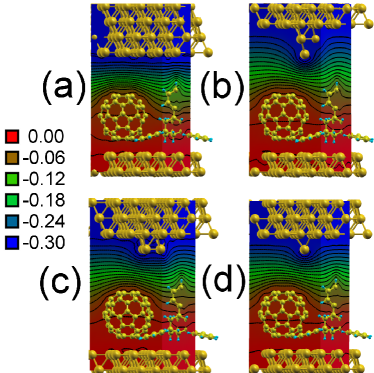
Figure 1 also shows the voltage drop across the tunneling junction when the external bias is 0.3 V. We see that most of the bias drop takes place in the vacuum region. At this bias, the LUMO lumo of C60 is close to the asymptotic chemical potential of the tip. Hence, C60 is largely conducting and the bias drop is smaller than in the vacuum gap: the voltage drops a tenth of the total bias just between the top of the molecule and the metallic substrate. The molecular states are then subjected to shift under the action of the bias. However, its partner TPA molecule has a large HOMO-LUMO gap which makes it basically inert. The voltage drop takes place across the molecule and it amounts to a seventh of the total bias. Hence, TPA behaves as the dielectric material of the molecular device that changes the charging energy of the active molecule, C60. Calculations with and without TPA show that the charging energy of C60 is reduced by 0.2 eV in the presence of TPA. Finally, as the tip becomes sharper, the electric field gets more localized. As a consequence, the electric field is large close to the tip and the voltage drop is faster in the vacuum gap while smaller at the molecular site. Hence, by sharpening the tip we obtain an effect similar to increasing the vacuum gap which enhances the tunneling-barrier bias dependence Tu .
The transmission behavior with applied bias varies rapidly as the tip changes. Figure 2 shows the electron transmission of Eq. (1) as a function of the electron energy , as the bias between tip and surface is increased. For a fixed bias, , the transmission function can be reproduced by a Breit-Wigner Datta formula:
| (2) |
The full-line curves in Fig. 2 are fits to Eq. (2) and dots are the Transiesta-evaluated transmissions. The agreement is excellent permitting us to extract the partial widths, and as well as the LUMO level as a function of applied bias, see Fig. 3.
The bias dependence of , Fig. 3, shows that the LUMO level is not pinned to the substrate’s electronic structure because the bias is not entirely droping in the vacuum gap. This is due to the molecule-molecule interactions of C60 with surrounding TPA, that decouple from the substrate and polarize C60. The flat-tip causes the largest shift both at zero-bias and at finite bias, showing that despite the 6.7-Å vacuum gap, there is interaction between molecule and tip. The tip also modifies the coupling of the molecule with the substrate. Indeed, the partial width due to the substrate, , can be divided in two values, Fig. 3, one corresponding to the blunt tips and and the other one to the atomic-like tips and . Due to the stronger coupling of the molecule with the Au(111) substrate, is larger and has a much smaller -dependence than that is the coupling with the tip. The behavior of with can be basically understood by the shift of the LUMO level, . As the bias increases, shifts closer to the vacuum level of the substrate, slightly increasing the partial width . However, is strongly dependent on the actual density of states (DOS) of the tip’s electronic structure. Sharp tips, and , show a non-monotonic behavior of with . This is also seen in the electron transmission since by virtue of Eq. (2), the transmission at is roughly proportional to .
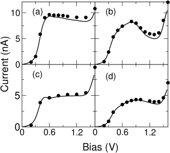
Figure 2 is the transmission function for the flat tip case. We see that the transmission maximum, corresponding to the LUMO, shifts to higher energies as the bias is increased. This is due to the partial bias drop at the center of the molecule and is reproducing the behavior described in Ref. Tu . More interestingly, the maximum height drops with bias. This is the behavior described in Ref. Grobis causing NDR. And indeed, as can be seen in Fig. 4 NDR is found for this system. This fast decay of the transmission is due to the increase of the tunneling barrier with increasing bias Grobis ; Tu .
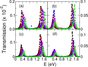
For the 4-atom pyramide tip, Fig. 2 , the maximum of the transmission peaks when the bias is at 0.8 V. This is totally different from the behavior of Fig. 2 and the one described in Ref. Grobis . The maximum of the transmission with bias can be traced back to a resonance of the 4-atom pyramidal tip of atomic origin. This is found at -0.45 eV in the DOS of the tip. Then, the strong variation of with bias, Fig 3, is due to the resonance in the DOS. When the tip is capped, Fig. 1 , the corresponding recovers a monotonic decrease with bias as for the flat-tip case , Fig. 3. Hence, the transmission is very similar to the case of the flat-tip. Finally, case where one adatom is added to the flat tip shows the same kind of non-monotonic behavior in as in and a clear maximum in both, and the transmission peaks for the LUMO around 0.8 V.
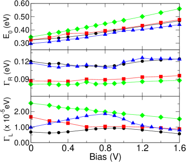
Figure 4 presents the – characteristics for the four systems of Fig. 1. The NDR features are large for the four-atom pyramidal tip, Fig. 4 and small for the flat tip, Fig. 4 . Hence, the largest NDR is obtained when the partial widths present a resonant behavior with the applied bias, as the one due to electronic resonances in the electrodes, tip . The monotonic bias dependence of partial widths due to the barrier dependence on the bias, case , is slower leading to weak NDR. It is interesting to study the capped pyramidal tip, Fig. 4 , where NDR is absent and the – curve is closer to the flat-tip one. Here, the partial width dependence is slow, Fig. 3, with increasing bias because the tip’s DOS is smoothly increasing. Despite the fact that the barrier height increases with bias, reducing the partial width, the increase of DOS is large enough to partially compensate the larger barrier and the transmission only drops slowly, Fig. 2 . NDR disappears. However, if one adatom is added to the flat tip, a bigger NDR effect is obtained because the sharper tip DOS forces a resonant-like and hence a peak-shaped transmission. It is then this last effect, rather than the enhancing of the bias dependence of the tunneling barrier, Fig. 1, that drives NDR in sharp tips.
The shape of the – characteristics changes with tip. While the flat tip has a sharp onset and a sharp peak at 0.6 V, the atom-terminated tips have a broad peak centered at 0.8 - 0.9 V with a 0.5-V width. The experimental one is a broad peak centered at 1.1 V with a 0.5-V width Franke . This fact and the current peak-to-valley ratio, Fig. 4, render the pyramidal tip in very good agreement with the experiment. Moreover, the experimental distance between the LUMO and LUMO+1 onsets Franke is 1.5 V and the one in Fig. 4 is 1.2 V. The actual – shape is then determined by the bias dependence of the level, , and of the partial widths, here . Indeed, the shape of, for instance, the LUMO onset is given by the -dependence of Gauyacq , while the NDR drop is dominated by the -dependence of .
In summary, we have performed NEGF calculations for the experimental setup of Ref. Franke . Our simulations have permitted us to rationalize the appearance of NDR in this system in terms of molecular levels and partial widths because we have been able to extract their bias dependence. We have shown that NDR can be tuned by modifying molecule-molecule and molecule-electrode interactions. The molecule-molecule interactions induce a reduction of the overwhelming presence of the substrate permitting us to have molecular properties with sizeable bias dependence. On the other hand, molecule-electrode interactions determine the molecular partial widths. NDR effects are maximum when the partial widths vary rapidly with the applied bias. This dependence is largest in the presence of electronic resonances on the electrodes such as the ones obtained for sharp STM tips. Finally, our results show that the overall shape of the – characteristic contains relevant information on the molecule-molecule and molecule-electrode interactions.
Acknowledgements.
We thank K. J. Franke and J. I. Pascual for very interesting discussions. F.D.N acknowledges support from Juan de la Cierva program. Computing resources from CESGA and financial support from the japanish JSPS, the spanish MICINN (FIS2009-12721-C04-01), and the european ICT project “AtMol” are gratefully acknowledeged.References
- (1) L. Esaki, Phys. Rev. 109, 603 (1958).
- (2) L. Chang, L. Esaki and R. Tsu, Appl. Phys. Lett. 24, 593 (1974).
- (3) S. M. Sze, Physics of Semiconductor Devices (Wiley, New York, 1981), p. 190.
- (4) A. Aviram and M. A. Ratner, Chem. Phys. Lett. 29, 277 (1974).
- (5) I. W. Lyo and P. Avouris, Science 245, 1369 (1989).
- (6) P. Bedrossian et al., Nature 342, 258 (1989).
- (7) J. Chen et al., Science 286, 1550 (1999).
- (8) C. G. Zeng et al., Appl. Phys. Lett. 77, 3595 (2000).
- (9) M. Rinkiö et al., ACS Nano 4, 3356 (2010).
- (10) X. Zheng et al., ACS Nano 4 , 7205 (2010).
- (11) M. Grobis et al., Appl. Phys. Lett. 86, 204102 (2005).
- (12) K. J. Franke et al., Phys. Rev. Lett. 100, 036807 (2008).
- (13) I. Fernández Torrente, K. J. Franke, and J. I. Pascual, J. Phys.: Condens. Matter 20, 184001 (2008).
- (14) Y. Xue et al., Phys. Rev. B 59, R7852 (1999).
- (15) L. Chen et al., Phys. Rev. Lett. 99, 146803 (2007).
- (16) X.Q. Shi et al. Phys. Rev. B 80, 075403 (2009).
- (17) X. W. Tu, G. Mikaelian, and W. Ho, Phys. Rev. Lett. 100, 126807 (2008).
- (18) R. Landauer, IBM J. Res. Dev. 1, 223 (1957).
- (19) M. Brandbyge et al, Phys. Rev. B 65, 165401 (2002); F. D. Novaes, A. J. R. da Silva and A. Fazzio, Brazilian Journal of Physics, 36, 799 (2006).
- (20) The LUMO of C60 is three-fold degenerate but there is only one LUMO contributing to the largest transmission eigenchannel.
- (21) Sandra García-Gil et al., Phys. Rev. B 79, 075441 (2009).
- (22) S. Datta, Electronic transport in mesoscopic systems (Cambridge University Press, Cambridge 1995).
- (23) S. Díaz-Tendero et al., Nano Lett. 8, 2712 (2008).