Manipulating the fully spin-polarized edge currents in graphene ribbon
Abstract
Electron fully spin-polarized edge states in graphene emerged at the interfaces of a nonuniform magnetic field are studied numerically in a tight-binding model, with both the orbital and Zeeman-splitting effects of magnetic field considered. We show that the fully spin-polarized currents can be manipulated by a gate voltage. In order to make use of the fully spin-polarized currents in the spin related transport, a three-terminal experiment is designed and expected to export the fully spin-polarized currents. This may have important applications in spin based nanodevices.
pacs:
72.25.-b, 73.20.-r, 71.70.DiI introduction
Recently, spin-dependent transport phenomena have received intensive studies because of their potential applications in spintronics devices. Understanding how to generate and manipulate the spin-polarized currents is one of the key points for the development of the spin-based devices. Rashba spin-orbit interaction, which can be controlled by an (or effective) electric field, provides an efficient way to achieve a spin-polarized current, for example in graphene ribbon,Zarea2009 doped semiconductorsKato2004 and 2D electron system.Sinova2004 In most of these applications, the induced charge currents are only partially polarized,Kane2005 but a fully spin-polarized (FSP) current is much more difficult to achieve experimentally. Up to now, FSP current is found to be realized only in very limited materials, for example, in the half-metallic states of the ferromagnetic metalsFerroMetA ; FerroMetB and ferromagnetic semiconductors,FerroSemA where the electronic valance band is partially filled for one spin component, whereas completely empty for the other. From material viewpoint, two-dimensional (2D) graphene, as a candidate material of new generation electronicsCastro Neto2009 ; Geim2007 ; Meyer2007 for its high mobility and low carrier density, is expected to have great application in spintronics devices.Cho2007 ; Tombros2007 ; Hill2007 ; Lundeberg2009 How to realize a FSP current in graphene is then quite meaningful for future graphene-based electronic devices. In graphene nanoribbon with zigzag edges, it has been predicted from a fist-principle calculationLouie2007 and numerical simulationsMac2009a ; Mac2009b that with the application of a transverse electric field, a half-metallic state can be achieved, which leads naturally to FSP edge currents propagating along sample boundaries.
On the other hand, for a 2D electron system, a sufficient strong magnetic field will polarize the spins of all electrons in the same direction as the field, but only a much smaller magnetic field is needed to achieve a FSP current.Xu2010 The cost is that a nonuniform magnetic field (NMF) must be applied to the system. Actually, it has been predicted that a partially spin-polarized current will appear at the interfaces of inhomogeneous magnetic fields,RamezaniMasir2008 ; Park2008 but much less attention are taken on the FSP states at the interfaces, especially, in graphene.
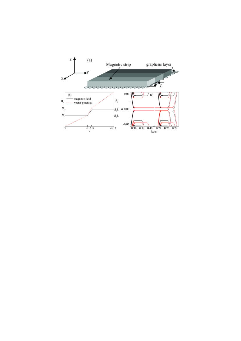
In this paper, we study monolayer graphene in the presence of a stepwise NMF, which can be realized experimentally in several ways,Cerchez2007 ; Leadbeater1995 ; Bending1990 to exhibit systematically how to manipulate the FSP currents generated at the interfaces of the NMF. The situation is schematically shown in Fig. 1(a). For the uniform magnetic field case, the FSP state is found to be absent, and the transport in graphene can be described by the so-called counter-propagating chiral edge states,Abanin2006 when the chemical potential is between the spin gap due to Zeeman splitting. However, for the stepwise NMF case, several spin gaps are opened and the FSP edge states may emerge at the magnetic interfaces when is between the gaps. In the following we will address the approach to manipulate this novel FSP edge currents. Furthermore, an experimental setup is designed to export the edge currents.
II model
We begin our discussion by the tight-binding model on a honeycomb lattice in the presence of a perpendicular magnetic field , which is given by,
| (1) |
where the first term describes electrons hopping between the nearest neighbors, suffering an additional phase caused by the orbital effect of magnetic field, with electron creation operators, whereas the second one the Zeeman splitting term. Here with as the Landé factor. The magnetic field is assumed to change only in direction, and the stepwise one which is focused on in this paper, has the following form,
| (2) |
For the gauge potential , the Landau gauge is adopted, with given as:
| (3) |
For simplicity, in the following discussion, energy is measured in unit of the hopping integral .
III results and discussions
To analyze all possible edge states, we choose open (periodic) boundary condition in the () direction, and numerically diagonalize the Hamiltonian on a rectangular sample under a NMF to obtain the electron energy spectrum. In one interface case, the spectrum is shown in Fig. 1(c), which is symmetric with respect to zero energy due to the particle-hole symmetry ( which, strictly speaking, should be combined with the time-reversal symmetry) preserved even in a NMF. The spectrum is composed of two series of Landau levels (LLs), including all the bulk states of the system, and branches of edge states, which play a dominant role in quantum transport in the presence of magnetic field. The edge states can be classified into the normal ones located at the sample boundaries, and the interface ones located at the interface where the magnetic field changes abruptly.
III.1 Generation and manipulation of the FSP edge currents
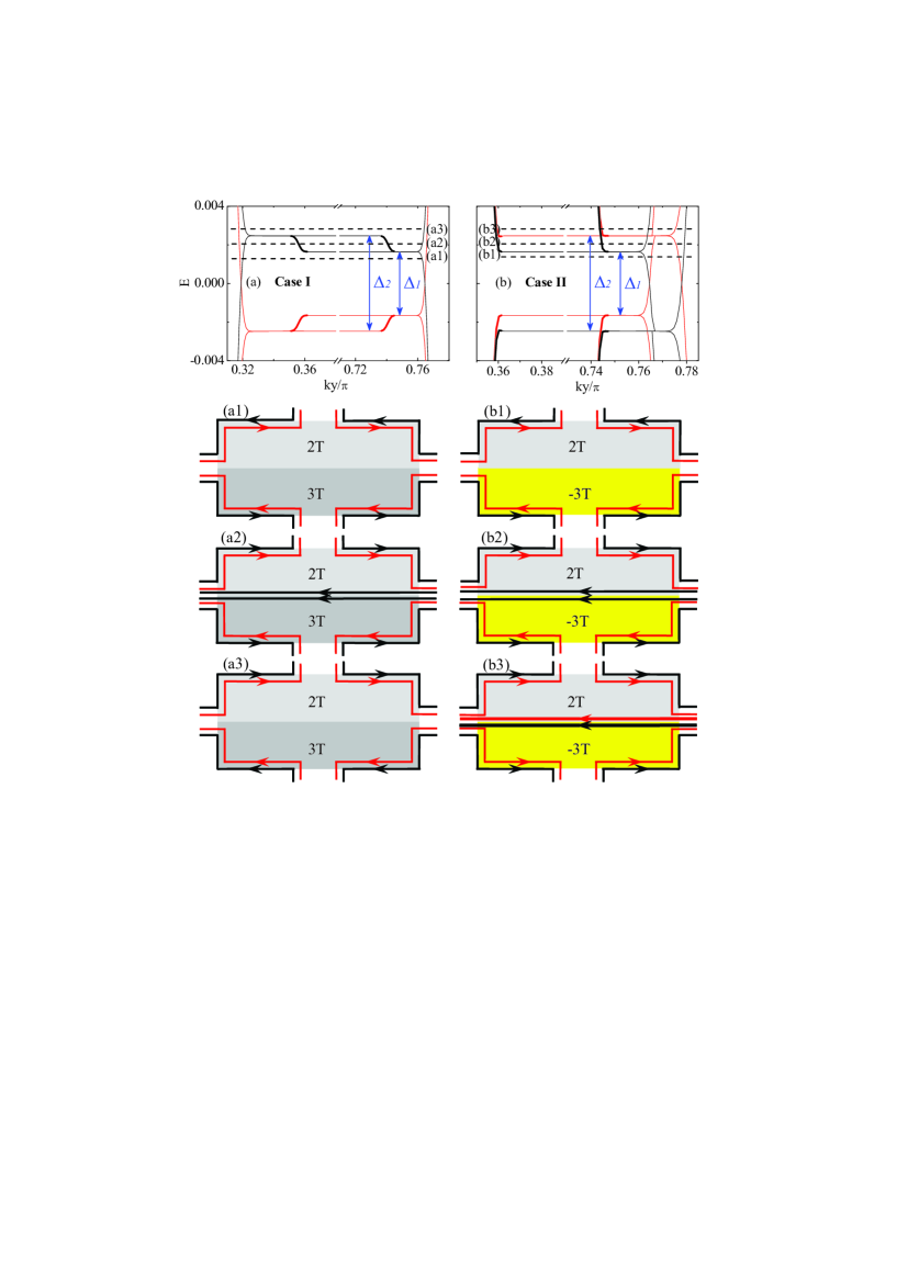
Let’s focus our discussion on the regime where the chemical potential is between the zeroth LLs of the two spin species. To make things more explicit, we show in Figs. 2(a) and 2(b) the energy spectrum around zero energy. The splitting of the zeroth LL and formation of two spin gaps and can be clearly seen. When lies within the interval or , there exist only sample boundary edge states, and no interface edge states at all. However, when lies between the two spin gaps , interface edge states are generated.
For , edge currents are propagating in opposite directions for opposite spin polarizations at both sample boundaries [see Fig. 2(a1)], which is similar to the quantum spin Hall state in graphene by considering intrinsic SO interaction,Kane2005 and also similar to the state predicted in Ref.Abanin2006, in a uniform magnetic field. For , however, the edge currents at sample boundaries become normal because they propagate in the same direction for both spin polarizations [see Fig. 2(a3)]. Interestingly, when the chemical potential lies within the gap , the interface channels are opened and two spin-down edge states with the same flowing direction emerge at the interface, and certainly, they are FSP [Fig. 2(a2)]. Meanwhile, the edge current at one sample boundary becomes normal whereas that at the other boundary is still left novel. For case where the magnetic fields in the two sides of the interface are in opposite directions, similar conclusion can be made except that when , no FSP state is present but the interface current channel is not closed and there exist a normal edge current at the interface instead [see Figs. 2(b1)-2(b3)].
From the viewpoint of application, one can use the properties mentioned above to manipulate the FSP edge currents. Imaging placing a voltage gate on the top of graphene sample, and by changing gradually the voltage, one can vary the carrier density in the sample, so the chemical potential gradually. We take Case I as an example. When lies within the minimum spin gap , the interface edge current channel is closed. As increases, the interface channel with a FSP edge current is opened if lies within the two gaps . Finally the channel is closed again in the interval . This implies that one can control the FSP edge currents electrically.
The spin gap due to Zeeman splitting is estimated as K at T, whereas the corresponding first LL is estimated to be about 500K. Furthermore, it was argued that the spin gap can be enhanced to a few hundred kelvin for a realistic magnetic field due to electron exchange interaction.Abanin2006 So the FSP current is expected to be observed experimentally in relatively large range of temperatures. To visualize the effect of the Zeeman splitting clearly and not changing the physics, relatively large spin gaps have been chosen for calculating the energy spectrum in Fig. 2. We also note that the localization character along direction for the edge states is well defined because the magnetic length here is nm, much less than the width of the sample (=213 nm).
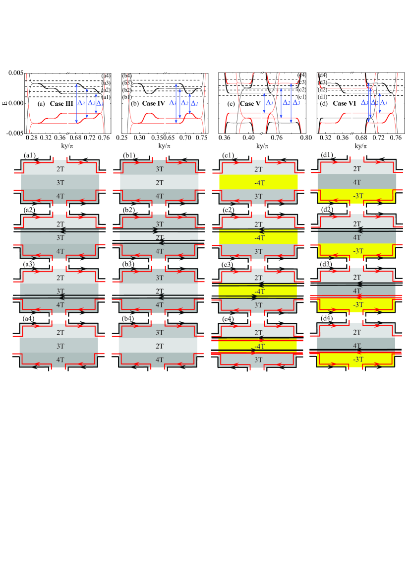
We next consider the case of NMF with two interfaces. There are twelve in total different configurations for pattern of magnetic field, but among them, only four( Case III- Case IV) are representative and of great interest, which is shown in Fig. 3. Three spin gaps are formed in each case, so similar to Fig. 2, the states between the zero LLs can be generally classified into four regimes, according to the position of the chemical potential .
Case III is very special. For this interesting case, if generally, there are more interfaces with the magnetic field in each region in the same direction and increasing monotonically, the FSP interface edge channels will be opened one by one from the low-field interface to high-field one, where the old one closing and new one opening happen simultaneously. For Case IV, when increases gradually from to , the two interface channels are opened simultaneously, after that one channel is closed and finally the other one is closed. For Case V and Case VI, although the FSP interface channels are opened and closed in different orders, these channels are not closed in the end but become normal ones instead [Figs. 3(c4) and 3(d4)].
Based on the above discussion, we come to a general conclusion that for a NMF with many interfaces, so long as the magnetic length is much less than the width of each uniform region, there always exist FSP edge states either at all the interfaces or at several of them, when the chemical potential lies within the gap . All the calculations above are performed for the zigzag graphene ribbon. For the armchair graphene ribbon, similar edge states and so similar conclusion can be obtained.
III.2 Rashba spin-orbit coupling effect
We now discuss the effect of the spin-flip processes caused by spin-orbit(SO) interaction. To estimate the influence of the SO interaction on the polarized edge current, we only consider here the Rashba SO interaction as an example, whose Hamiltonian can be written as
| (4) |
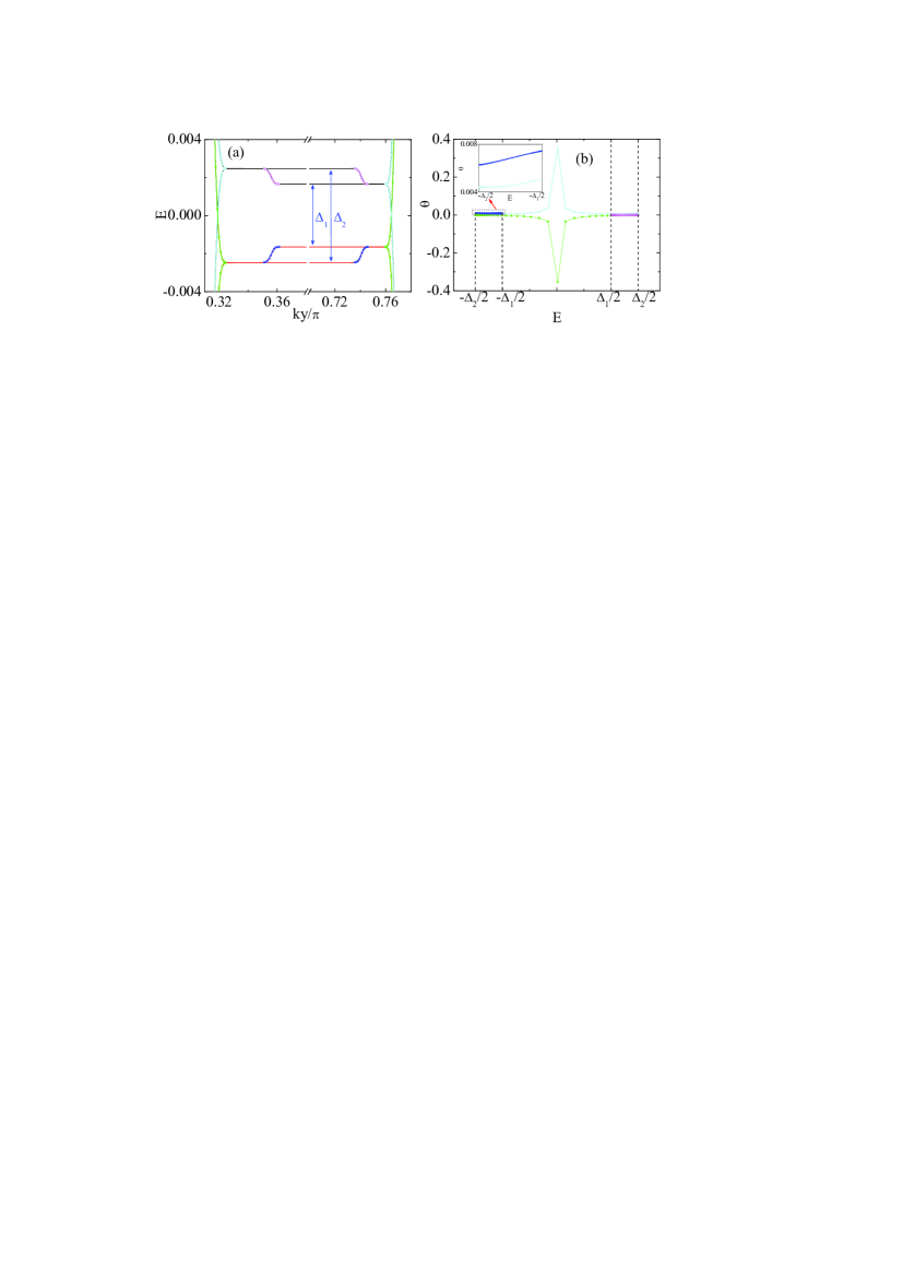
where is the Rashba SO coupling strength and is the Pauli matrix. is a vector pointing from to its nearest neighbor , and is a unit vector in direction. Figure 4 (a) shows the spectrum at low energies with Rashba SO interaction, which is found to be almost unchanged compared with the case without SO coupling [Fig. 2 (a)]. However, in contrast to the case without SO interaction where electrons are polarized along axis, the spin polarization of the edge states in the presence of the SO interaction can be described by with the tilting angle deviated from the z axis, changing continuously with . Therefore, theoretically speaking, the FSP interface current is still preserved at K [Fig. 4 (a)], except that the edge current is now polarized along other direction instead which slight deviates from axis by an angle . In the spin gap region , for the parameters shown in Fig.4, the tilting angle for the interface edge states is estimated to be . It is very small and changes nearly linearly with energy with the slope in this gap [see the inset in Fig. 4 (b)]. Physically, the slope is believed to be nearly proportional to , which is rather small in real situations (For a perpendicular electric field V nm,Kane2005 ; Novoselov2004 K.Huertas2006 ; Min2006 ). At finite temperatures, in order to obtain a almost FSP interface current, the thermodynamical energy should be much less than the spin gap , which is estimated to be about K for T.Abanin2006 Therefore, in many situations achievable in experiments, the spin-flip processes induced by the Rashba SO interaction can be negligible, and an almost FSP current can be realized.
III.3 Exporting the FSP edge currents
So far, we have shown explicitly how to generate and manipulate the FSP edge currents, but another associated and interesting question which naturally arises is still unsolved, which is how to export the FSP current to serve as a current source for a spin related device. This is not a trivial question, because to export the current, one has to destroy the interface in some extent to introduce another lead, but the FSP current is composed of edge states, which will disappear when the interface is destroyed or removed away. For this purpose, we design an experimental setup shown schematically In Fig. 5(a), which is expected to export FSP current to the possible spin related device connected with the armchair graphene sample by a narrow graphene strip. Here the armchair graphene ribbon is adopted, because for the zigzag graphene ribbon, the existence of the flat edge bands will cause ferromagnetic instability and lead to local ferromagnetic polarizations at sample edges,Fujita1996 giving rise to spin-flip processes.
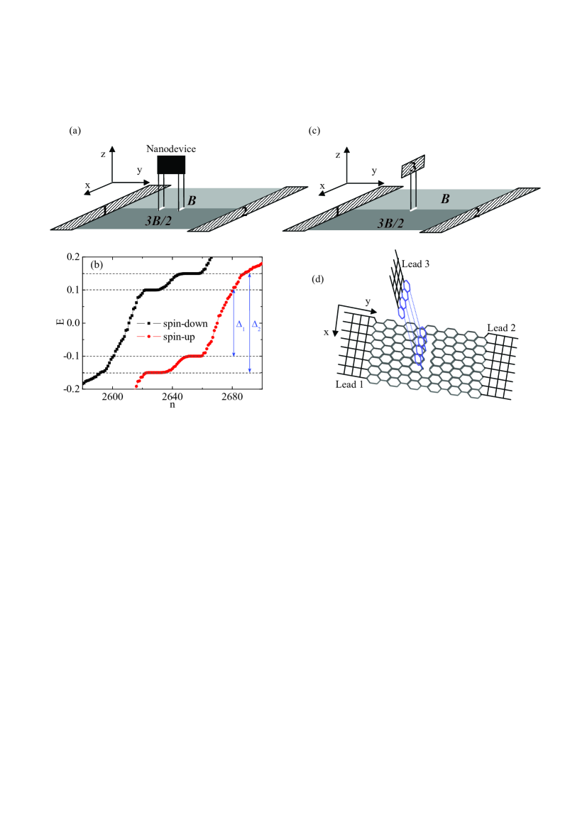
To testify this idea, we first calculate the eigenvalues of this particular system for an open boundary condition. We find that LLs are still present even in the condition that the interface is partially destroyed by the introduced lead. However, states for both spin species exist between the LLs [Fig. 5(b)], leaving the question whether spin-up electrons in this regime contribute to the current flowing through the device still unaddressed. Therefore, in order to confirm that the current flowing through the device is FSP, we refer to the three-terminal setup as illustrated in Fig. 5(c), where the rectangular graphene sample is connected with three ideal semi-infinite leads. The detail of these connections between graphene sample and the leads is shown in Fig. 5(d). In this situation, four bonds across the interface are broken, so that lead 3 made of the narrow graphene strip can be connected with the sample. This strip is then upright so as to avoid the influence of magnetic field. According to the Fisher-Lee relation, the electron transmission coefficient from lead to lead for multi-terminal Landauer-Büttiker formula is given byHankiewicz2004 ; Sheng2005
| (5) |
The scattering rate matrix due to the coupling to lead has a form
| (6) |
where is the self-energy due to lead p and the elements of the matrix are given by
| (7) |
with the function describing the transverse profile of mode in lead and the wave vector determined by the equation . Here is the number of sites connected with the leads and . The retarded Green’s function of the graphene sample is written as
| (8) |
and . Here, to make the calculation simple, the three leads are assumed to be described by a nearest-neighbor tight-binding model on a square lattice with the same hopping integral as graphene.
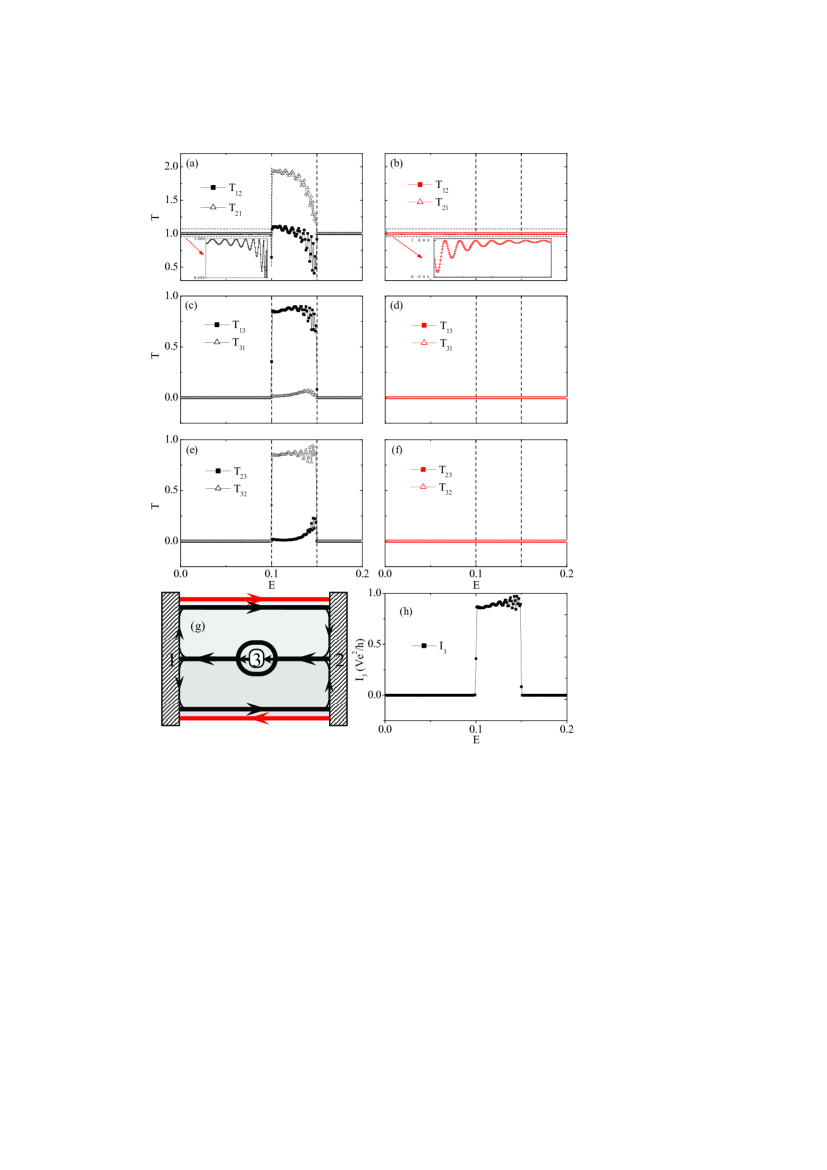
The transmission coefficients are plotted in Fig. 5. For spin-up electrons, and show quasi-periodic oscillation and the maxima of them are the quantized value 1. This oscillating behavior is similar to that found in graphene-based ferromagnetic double junctions,Bai2010 and can be attributed to electrons’ multiple reflections between terminal 1 and 2. As the energy increases gradually from 0 to 0.2, both and are approaching to 1, suggesting one left-moving spin-up edge state on one sample boundary and one right-moving one on the other, sharing the similar picture with Fig. 2(a). However, most importantly, we find that within the error range, and in the whole energy range we are interested in. This is corresponding to the absence of spin-up edge states at the interface.
For spin-down electrons, when and , , the situation is similar to that for spin-up electrons. However, when , and show strongly fluctuations, and deviate from the quantized value 2 [Fig. 6(a)], which should be taken in the ideal case shown in Fig. 2(a). This may be ascribed to the bonds breaking at the interface of terminal 3, and lattice mismatching at the interfaces of terminal 1and 2 which results in electrons scattering from edges states to the nearby zeroth LL [see Fig. 5(b)]. In the same range, the fact that and indicates that both the left- and right-moving currents exist, but the net current is left moving. The finiteness of also implies that a small fraction of spin-down electrons incoming from terminal 3 have to be scattered to sample boundaries via bulk states, since there is no current channel at the interface from terminal 3 to 2. Similarly, the finiteness of means that the right-moving spin-down electrons propagating along sample boundaries have some probability to be scattered to terminal 3 via bulk states. These processes are schematically shown in Fig. 6(g). We remark that although these scattering processes will cause resistance, spin is conserved since there is no spin-flip processes considered here. This leads to the conclusion that the electron current flowing out of terminal 3 has spin-down polarization, and so is FSP.
In actual application, one can apply the electrical voltage to the three terminals as and , then the FSP (spin-down) electrons will be transported from lead 3 to leads 1 and 2. In this situation, the FSP current flowing out of terminal 3, is estimated as [see Fig. 6(h)]. Indeed, the width of the strip is nm and the magnetic length is about nm. The fact of guarantees that there are sufficient electrons through the strip. Therefore, the graphene sample with the designed setup under a NMF can be viewed as the FSP current source for a spin related nanodevice.
IV summary
In summary, we have numerically investigated the FSP edge currents at the interface in graphene under a nonuniform magnetic field. The manipulation of the FSP currents is realized by a gate voltage, and its potential application in spintronic devices is also discussed. An experimental setup is designed and is expected to export the FSP current, which is confirmed numerically by a three-terminal transmission calculation.
Acknowledgements.
The author J. An thanks X. G. Wan, H. H. Wen, J. X. Li, Q. H. Wang for useful discussions. This work was supported by NSFC Projects No. 10504009, and No. 10874073, and 973 Projects No. 2006CB921802, No. 2006CB601002, and No. 2009CB929504.References
- (1) M. Zarea and N. Sandler, Phys. Rev. B 79, 165442 (2009).
- (2) Y. K. Kato, R. C. Myers, A. C. Gossard, D. D. Awschalom, Science 306, 1910 (2004).
- (3) J. Sinova, D. Culcer, Q. Niu, N. A. Sinitsyn, T. Jungwirth, and A. H. MacDonald, Phys. Rev. Lett. 92, 126603 (2004).
- (4) C. L. Kane and E. J. Mele, Phys. Rev. Lett. 95, 226801 (2005).
- (5) R. A. de Groot, F. M. Mueller, P. G. van Engen, and K. H. J. Buschow, Phys. Rev. Lett. 50, 2024 (1983).
- (6) J-H. Park, Nature 392, 794 (1998).
- (7) K. R. Kittilstved, D. A. Schwartz, A. C. Tuan, S. M. Heald, S. A. Chambers, and D. R. Gamelin, Phys. Rev. Lett. 97, 037203 (2006).
- (8) A. H. Castro Neto, F. Guinea, N. M. R. Peres, K. S. Novoselov, and A. K. Geim, Rev. Mod. Phys. 81, 109 (2009).
- (9) A. K. Geim and K. S. Novoselov, Nat. Mater. 6, 183 (2007).
- (10) J. C. Meyer et al., Nature (London) 446, 60 (2007).
- (11) S. Cho, Yung-Fu Chen, and M. S. Fuhrerb, Appl. Phys. Lett. 91, 123105 (2007).
- (12) N. Tombros, C. Jozsa, M. Popinciuc, H. T. Jonkman, and B. J. van Wees, Nature (London) 448, 571 (2007).
- (13) E. W. Hill, A. K. Geim, K. S. Novoselov, F. Schedin, and P. Blake, IEEE Trans. Magn. 42, 2694 (2007).
- (14) M. B. Lundeberg and J. A. Folk, Nat. Phys. 5, 894 (2009).
- (15) Y-W. Son, M. L. Cohen, and S. G. Louie, Nature. 444, 347 (2006).
- (16) J. Jung, T. Pereg-Barnea, and A. H. MacDonald, Phys. Rev. Lett. 102, 227205 (2009).
- (17) J. Jung and A. H. MacDonald, Phys. Rev. B 79, 235433 (2009).
- (18) L. Xu, J. An, and C.-D. Gong, Phys. Rev. B 82, 155421 (2010).
- (19) M. Ramezani Masir, P. Vasilopoulos, A. Matulis, and F. M. Peeters, Phys. Rev. B 77, 235443 (2008).
- (20) S. Park and H.-S. Sim, Phys. Rev. B 77, 075433 (2008).
- (21) M. Cerchez, S. Hugger, T. Heinzel, and N. Schulz, Phys. Rev. B 75, 035341 (2007), and references therein.
- (22) M. L. Leadbeater, C. L. Foden, J. H. Burroughes, M. Pepper, T. M. Burke, L. L. Wang, M. P. Grimshaw, and D. A. Ritchie, Phys. Rev. B 52, R8629 (1995).
- (23) S. J. Bending, K. von Klitzing, and K. Ploog, Phys. Rev. Lett. 65, 1060 (1990).
- (24) D. A. Abanin, P. A. Lee, and L. S. Levitov, Phys. Rev. Lett. 96, 176803 (2006).
- (25) D. Huertas-Hernando, F. Guinea, and A. Brataas, Phys. Rev. B 74, 155426 (2006).
- (26) H. Min, J. E. Hill, N. A. Sinitsyn, B. R. Sahu, Leonard Kleinman, and A. H. MacDonald, Phys. Rev. B 74, 165310 (2006).
- (27) K. S. Novoselov, A. K. Geim, S. V. Morozov, D. Jiang, Y. Zhang, S. V. Dubonos, I. V. Gregorieva, and A. A. Firsov, Science 306, 666 (2004).
- (28) M. Fujita, K. Wakabayashi, K. Nakada, and K. Kusakabe, J. Phys. Soc. Jpn. 65, 1920 (1996).
- (29) L. Sheng, D. N. Sheng, and C. S. Ting, Phys. Rev. Lett. 94, 016602 (2005).
- (30) E. M. Hankiewicz, L.W. Molenkamp, T. Jungwirth, and J. Sinova, Phys. Rev. B 70, 241301(R) (2004).
- (31) C. Bai, J. Wang, S. Jia, and Y. Yang, Appl. Phys. Lett. 96, 223102 (2010).
- (32) E. Prada, P. San-Jose, and L. Brey, Phys. Rev. Lett. 105, 106802 (2010).