Purcell factor for point–like dipolar emitter coupling to 2D-plasmonic waveguides
Abstract
We theoretically investigate the spontaneous emission of a point–like dipolar emitter located near a two–dimensional (2D) plasmonic waveguide of arbitrary form. We invoke an explicite link with the density of modes of the waveguide describing the electromagnetic channels into which the emitter can couple. We obtain a closed form expression for the coupling to propagative plasmon, extending thus the Purcell factor to plasmonic configurations. Radiative and non-radiative contributions to the spontaneous emission are also discussed in details.
pacs:
42.50.Pq, 42.50.Nn, 73.20.Mf , 42.82.-m, 32.50.+dIn 1946, Purcell demonstrated that spontaneous emission of a quantum emitter is modified when located inside a cavity Purcell (1946). A critical parameter is the ratio , where Q and refer to the cavity mode quality factor and effective volume, respectively. In the weak coupling regime, the Purcell factor , quantifies the emission rate inside the cavity compared its free-space value
| (1) |
where is the emission wavelength and the cavity optical index. When is high enough, strong coupling regime occurs with reversible energy exchange between the emitter and the cavity mode (Rabi oscillations) Vahala (2003). The design of cavities maximizing this ratio in order to control spontaneous emission is extremelly challenging. There is however a trade-off between Q factor and effective volume. On one side, ultra high Q () are obtained in microcavities but with large effective volume (). On the other side, diffraction limited mode volume [] are achieved in photonic crystals but at the price of weaker quality factors (). Moreover, it is sometimes preferable to optimize but keeping a reasonable Q factor in order to efficiently extract the signal from the cavity. Additionally, the emitter spectrum can be large at ambiant temperature and better coupling is expected with low Q cavities Maksymov et al. (2010) (i.-e. matching cavity and emitter impedances Greffet-Laroche-Marquier:2010 ).
In this context, it has been proposed to replace the cavity (polariton) mode by a surface plasmon polariton (SPP) sustained by metallic structures as an alternative to cavity quantum electrodynamics Chang et al. (2006); Cuche-Mollet-Drezet-Huant:2010 . SPP can have extremelly reduced effective volume, insuring high coupling rate with quantum emitters, albeit a poor quality factor ( Cavity ). Particularly, coupling an emitter to a plasmonic wire shed new light on manipulating single photon source at a strongly subwavelength scale, with applications for quantum information processing qbits . Others promissing applications deal with the realization of integrated plasmonic amplifier De Leon and Berini (2008); Grandidier et al. (2009); G. Colas des Francs et al. (2010a). Highly resolved surface spectroscopy was also pointed out based either on the antenna effect Zuev et al. (2005) or coupling dipolar emission to an optical fiber via a plasmonic structure Tanaka et al. (2008); Chen et al. (2009).
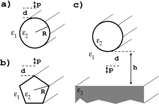
In this work, we present an original approach for calculating rigorously the coupling of dipolar emitter to 2D plasmonic waveguides of arbitrary profile. We achieve a closed form expression for the coupling rate into the guided SPP. We also investigate the radiative and non radiative channels. In particular, the contribution of the plasmon, difficult to estimate otherwise Chang et al. (2006); Issa and Guckenberger (2007), is clearly established. Our method is general and treat equivalently bound and leaky waveguides of arbitrary cross-section, possibly on a substrate (Fig. 1).
According to Fermi’s golden rule, coupling of a quantum emitter to a continuum of modes is governed by the (3D) local density of states (3D-LDOS)
| (2) |
where is the local density of modes, projected along the direction of the dipolar transition moment (partial LDOS) PLDOS . is the emitter location and its emission frequency. To characterize the coupling independantly of the emitter properties, we introduce the normalized quantity where is the free-space partial LDOS.
Since we are interested in 2D waveguide, the main idea is to work on the density of modes associated with the guide (bound and radiation modes). For this purpose, we now establish a relationship between 2D and 3D LDOS by introducing Green’s dyad formalism. First, the 3D-LDOS is related to the 3D Green’s tensor of the system ( and refer to the imaginary part and trace) G. Colas des Francs et al. (2001)
| (3) |
In presence of an infinitely long (2D) structure, the 3D-Green’s tensor is expressed by a Fourier transform
| (4) |
Then, we obtain the 3D-LDOS as a function of 2D-Green’s dyad
| (5) |
Equation (5) obviously reproduces the 3D-LDOS in a homogeneous medium of index . Limiting the integration range to radiative waves, and since in a homogeneous medium, we obtain, as expected, . The quantity is generally referred as 2D-LDOS by analogy with 3D-LDOS expression (3) 2DLDOS . It is a key quantity to understand spatially and spectrally resolved electron energy loss spectroscopy García de Abajo and Kociak (2008). Equation (5) makes then a direct link between 2D and 3D LDOS. We however consider a slightly different definition, more appropriate to describe a density of guided modes Gérard Colas des Francs et al. (2009)
| (6) |
The 2D Green’s dyad is separated in two contributions where is the 2D-Green’s dyad without the waveguide and is the guide contribution. This formulation separates the reference system (multilayer substrate, homogeneous background, …) from the guiding structure. It comes, with the dielectric constant of the reference system,
| (7) | |||||
This wording separates the continuum of modes of the reference system from the waveguide density of modes . The partial 2D-LDOS is finally
| (8) |
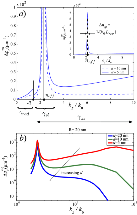
Figure 2 represents the radial 2D-LDOS for the benchmark model defined in Fig. 1a). 2D-Green’s dyad has been numerically evaluated by applying a meshing on the waveguide cross-section Gérard Colas des Francs et al. (2009). The main contribution is the Lorentzian variation peaked at the effective index of the guided SPP , and with a full width at half maximum inversely proportional to the mode propagation length m (inset). For , the 2D-LDOS describes scattering events and contributes to radiative rate . Finally, for , LDOS takes part to the non-radiative decay rate . Indeed, the plasmon is dissipated by thermal losses. Moreover, for very short distances, the 2D-LDOS spectrum extends over very large values of (Fig. 2b). This behaviour is typical for non-radiative transfer by electron-hole pairs creation in the metal Barnes (1998).
The coupling rate into the propagative SPP is obtained using equations (3,5,8) and keeping only the plasmon contribution by limiting the integration of Eq. (5) to corresponding to the SPP resonance. This is strongly simplified by the Lorentzian shape of the resonance and leads to the closed form expression G. Colas des Francs et al. (2010a)
| (9) |
This important result describes the emitter coupling rate to a 2D waveguide of arbitrary cross section. It is expressed as the overlap between the dipolar emission and the guided mode profile () divided by the mode propagation length in the longitudinal direction. This defines the 3D Purcell factor for a 2D geometry. Although presented for plasmonic waveguide, the demonstration remains valid for any 2D configuration (plasmonic cavity Cavity or waveguide G. Colas des Francs et al. (2010a), metal coated Maksymov et al. (2010) or dielectric Kien et al. (2005) nanofiber, …). In order to validate this expression, we now compare it to the exact expression obtained by considering coupling to a lossless waveguide Kien et al. (2005); Chen et al. (2010):
| (10) |
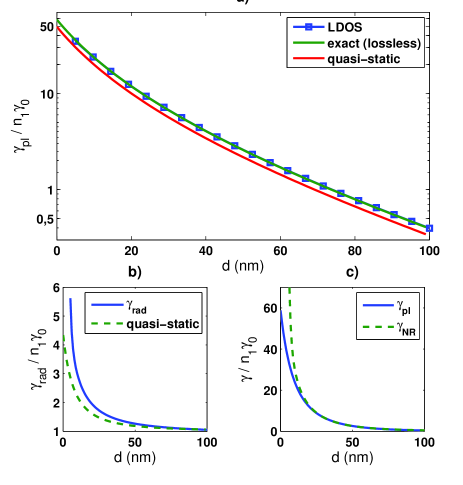
where is the electromagnetic field associated with the guided SPP. In Fig. 3a), we compare the coupling rate into the plasmonic channel as a function of distance to the silver nanowire obtained using i) closed form expression (9), ii) exact expression for a lossless plasmonic waveguide (10) and iii) a quasi-static approximation Chang et al. (2006).
Quite surprinsingly, although the exact expression neglects dissipation, we obtain an excellent agreement with our expression that correctly accounts for losses. In formula (9) the ratio is proportional to the number of guided modes Gérard Colas des Francs et al. (2009) so that it does not depends on the losses. When losses tends towards zero, and at resonance so that remains constant (Dirac distribution). Equivalently, this simply reveals that the emitter couples to the guided mode, no matter if the energy is dissipated by losses during propagation or propagates to infinity.
We now turn on the radiative decay rate associated with the 2D-LDOS in the interval . We compare in Fig. 3b) our numerical simulation with quasi-static approximation derived in Ref. Klimov et al. (2004); Chang et al. (2006) for the nanowire. The quasi-static approximation underestimates the radiative contribution to the coupling rate since it only considers the cylindrical dipole mode.
Finally, the non-radiative decay rate is determined from 2D-LDOS calculated on the evanescent domain which includes all the non radiative mechanisms: Joule losses during plasmon propagation and electron-hole pairs creation into the metal. Figure 3c) represents the plasmon and total non radiative rates. The non-radiative rate diverges close to the wire surface whereas plasmon contribution remains finite. For large separation distances, the plasmon is the only contribution to the non radiative rate. We achieve an optimal coupling efficiency into the guided SPP, , at .
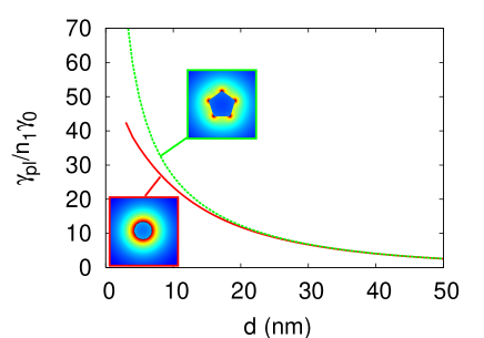
So far, we considered a silver circular nanowire embedded in a homogeneous background to illustrate and validate our method. In the following, we investigate the two complex geometries depicted on Fig. 1b,c). Figure 4 presents the coupling rate into the SPP supported by a penta-twinned crystalline nanowire recently characterized Song et al. (2011). At short distances, the coupling rate into the guided SPP is strongly enhanced as compared to coupling to a circular wire of similar dimensions. This is due to the strong mode confinement near the wire corners as revealed by the mode profile.
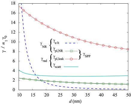
Experimental configurations generally concern structures deposited on a substrate. For high index substrate, the otherwise bound mode becomes leaky. Note that usual expression (10) is then practically unenforceable due to difficulty of normalizing the mode. Differently, expression (9), derivated in this work, is easily used even in such a situation. Moreover, in case of leaky mode, it is even more difficult to properly distinguish radiative and non radiative contributions to the coupling rate, as compared to the bound mode situation treated above. Indeed, the guided plasmon contributes to both the radiative rate (leaky part) and non radiative transfer (intrinsic losses). This difficulty is easily overcome using the 2D-LDOS formalism. The propagation length can be written where the radiative and non radiative rates have been introduced. As an example, we consider a 100 nm silver wire 50 nm above a glass substrate. We calculate an effective index , below the substrate optical index, indicating a leaky mode. Its propagation length is with . The leakage rate is evaluated by cancelling the metal losses (). We obtain . Figure 5 shows the interplay between the various contributions to the decay rate for an emitter placed in the wire-substrate gap. The radiative rate is the sum of the scattering and leakage channels and the non radiative rate originates from plasmon losses and electron-hole pairs creation. Except for short distances, the main decay channel is the plasmon decoupling into the substrate. We obtain a maximum decoupling emission into the substrate for an emitter centered in the gap () MallekZouari et al. (2010).
To conclude, we derive an explicit expression for the coupling rate between a point–like quantum emitter and a 2D plasmonic waveguide. We define the coupling Purcell factor into the plasmon channel whereas the radiative and non radiative rates are numerically investigated. This method clearly reveals the physics underlying the complex mechanisms of spontaneous emission coupled to a plasmonic guide (scattering, leakage, electron-hole pairs creation, SPP excitation).
This work is supported by French National Agency (ANR PlasTips and -Plas). Calculations were performed using DSI-CCUB resources (Université de Bourgogne).
References
- Purcell (1946) E. Purcell, Phys. Rev. 69, 681 (1946).
- Vahala (2003) K. Vahala, Nature 424, 839 (2003).
- Maksymov et al. (2010) I. Maksymov et al., Phys. Rev. Lett. 105, 180102 (2010).
- (4) J.J. Greffet et al., Phys. Rev. Lett. 105, 117701 (2010).
- Chang et al. (2006) D. Chang et al., Phys. Rev. Lett. 97 053002 (2006).
- (6) A. Cuche et al., Nano Lett. 10 4566–4570 (2010).
- (7) J.-C. Weeber et al., Nano Lett. 7, 1352 (2007). Y. Gonga and J. Vuckovic, Appl. Phys. Lett. 90, 033113 (2007).
- (8) D. Chang et al., Nat. Phys. 3 807–812 (2007). D. Dzsotjan et al., Phys. Rev. B 82, 075427 (2010). A. Gonzalez-Tudela et al., Phys. Rev. Lett 106, 020501 (2011).
- De Leon and Berini (2008) I. De Leon and P. Berini, Phys. Rev. B 78, 161401 (2008).
- Grandidier et al. (2009) J. Grandidier et al., Nano Lett. 9, 2935 (2009).
- G. Colas des Francs et al. (2010a) G. Colas des Francs et al., Opt. Exp. 18, 16327 (2010a).
- Zuev et al. (2005) V. Zuev et al., J. Chem. Phys. 122, 214726 (2005).
- Tanaka et al. (2008) K. Tanaka et al., Appl. Phys. B 93, 257 (2008).
- Chen et al. (2009) X. Chen al, Nano Lett. 9, 3756 (2009).
- Issa and Guckenberger (2007) N. Issa and R. Guckenberger, Opt. Exp. 15, 12131 (2007).
- (16) G. Colas des Francs et al, J. Chem. Phys. 117, 4659 (2002). J. Hoogenboom et al, Nano Lett. 9, 1189 (2009).
- G. Colas des Francs et al. (2001) Colas des Francs et al., Phys. Rev. Lett. 86, 4950 (2001).
- (18) O. Martin et al., Phys. Rev. Lett. 82, 315 (1999). A. Asatryan et al., Phys. Rev. E 63, 046612 (2001).
- García de Abajo and Kociak (2008) J. García de Abajo and M. Kociak, Phys. Rev. Lett. 100, 106804 (2008).
- Gérard Colas des Francs et al. (2009) G. Colas des Francs et al., Phys. Rev. B 80, 115419 (2009).
- Barnes (1998) W. Barnes, J. Mod. Opt. 45, 661 (1998).
- Kien et al. (2005) F. Kien et al., Phys. Rev. A 72, 032509 (2005).
- Chen et al. (2010) Y. Chen et al., Phys. Rev. B 81, 125431 (2010).
- Klimov et al. (2004) V. Klimov et al, Phys. Rev. A 69, 013812 (2004).
- Song et al. (2011) M. Song et al, ACS Nano , ASAP (2011).
- MallekZouari et al. (2010) I. Mallek Zouari et al, Appl. Phys. Lett. 97, 053109 (2010).