Phase qubits fabricated with trilayer junctions
Abstract
We have developed a novel Josephson junction geometry with minimal volume of lossy isolation dielectric, being suitable for higher quality trilayer junctions implemented in qubits. The junctions are based on in-situ deposited trilayers with thermal tunnel oxide, have micron-sized areas and a low subgap current. In qubit spectroscopy only a few avoided level crossings are observed, and the measured relaxation time of is in good agreement with the usual phase qubit decay time, indicating low loss due to the additional isolation dielectric.
pacs:
74.50.+r, 85.25.Cp, 85.25.-j1 Introduction
The energy relaxation time of superconducting qubits is affected by dielectric loss, nonequilibrium quasiparticles [1], and charge or bias noise, and varies between a few nano- to several microseconds, depending on qubit type, material, and device layout. Superconducting qubits are commonly based on thin films, and their central element, the non-linear inductor given by a Josephson tunnel junction (JJ), is formed either by overlap [2] or window-type geometries [3]. Qubit spectroscopy reveals coupling to stochastically distributed two-level systems (TLSs) in the tunnel oxide [4, 5, 6, 7, 8] which provide a channel for qubit decoherence. While the physical nature of TLSs is still under debate, their number was shown to decrease with junction size and their density with higher atomic coordination number of the tunnel oxide [3, 9]. The number of coherent oscillations in the qubit is limited by, among other decoherence mechanisms such as nonequilibrium quasiparticles, the effective dielectric loss tangent [9]. The overlap geometry provides JJs with amorphous barriers with no need for isolation dielectrics, being itself a source for additional TLSs and dielectric losses. The window geometry is used for higher quality, e.g. epitaxial, trilayer JJs with in-situ grown barriers. Besides complex fabrication, they have the drawback of requiring additional isolation dielectrics [10]. The importance of keeping the total dielectric volume in qubits small to reduce the additional loss was shown in Ref. [9].
In this paper we give an overview of our standard technology for junction fabrication, and present an alternative junction based on sputtered trilayer stacks, which provide an intrinsically cleaner tunnel oxide and is well suited for micron-sized trilayer qubit junctions. The so-called side-wall passivated JJs provide contact to the top electrode without adding too much lossy dielectric to the circuitry, which would negatively affect the loss tangent. The trilayer isolation is achieved via an electrolytic process. These novel JJs were realized in a flux-biased phase qubit and characterized by i) current transport measurements on reference junctions and ii) spectroscopy and time-domain measurements of the qubit.
By systematically replacing only the Josephson junction, being central to any superconducting qubit, we aim to analyze the loss contributions of this specific element, and, ideally, develop low-loss Josephson junctions for superconducting qubits and improve our qubit performance. We found performance comparable to the current generation of overlap phase qubits.
2 Novel geometry
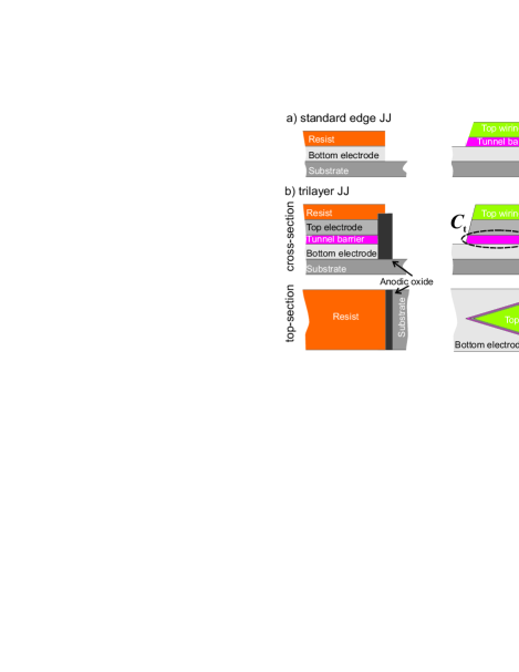
Figure 1 depicts the patterning process for our standard overlap (a) and trilayer junctions (b). Our standard process has an oxide layer grown on an ion mill cleaned aluminum edge, which was previously chlorine etched. The top wiring is then etched back below the oxide layer using argon with chlorine mixture. For the trilayer process, the in-situ sputtered -- trilayer has a thermally grown tunnel oxide barrier, formed for 10 min at at room temperature. After deposition of the trilayer stack an edge is etched. The bottom electrode of the trilayer stack is isolated from the top electrode wiring by a self-aligned nanometer thin dielectric layer, grown for (or other suitable electrode metals such as ) by anodic oxidation [11]. The metallic aluminium serves as partly submerged anode in a liquid electrolytic mixture of ammonium pentaborate, ethylene glycol
and at room temperature. A gold-covered metal served as cathode and the electric contact was made outside the electrolyte to the anode. By protecting parts of the aluminum electrode with photoresist only a well-defined area was oxidized by passing a constant current through the Al film and converting the metallic surface to its oxide form. The oxide thickness can be controlled by the voltage drop across the electrolyte. After a light ion clean and top wiring deposition the resist is patterned to define the junction area. Finally, the trilayer is etched below the tunnel barrier, yielding Josephson junctions with planar tunnel barrier and isolation dielectric on just one side of the tunnel area. For junctions a similar patterning process, without minimizing the dielectric loss contribution, was developed using anodic oxide and covered by [12]. The in-situ grown tunnel oxide avoids sources of residual impurities such as hydrogen, hydroxide or carbon at the interface vicinity, which may remain even after ion-milling in our standard process. These trilayer junctions are fully compatible with our standard process using overlap patterning and no junction side-wall.
2.1 Transport
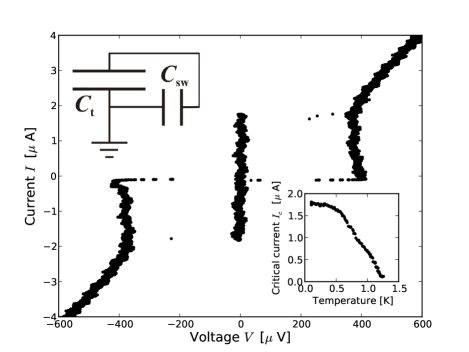
Transport measurements on a reference junction at are shown in Fig. 2. The critical current is , with normal resistance yielding , close to the calculated Ambegaokar-Baratoff value of for the measured superconducting gap of . The back bending of the voltage close to the gap voltage is attributed to self-heating inside the junction. The retrapping current of indicates a very small subgap current. The current transport is consistent with tunneling, and we can exclude transport via metallic pinholes, located in the thin side-wall dielectric. As a further check, the dependence is as expected, see inset in Fig. 2, with a critical temperature of .
3 Measurement
The qubit is a flux-biased phase qubit that is coupled via a tunable mutual inductance to the readout-SQUID [13]. The total qubit capacitance , see upper inset of Fig. 3, is given by the tunnel oxide , the anodic side-wall oxide and shunt capacitor dielectric, provided by a parallel plate capacitor with relative permittivity made from hydrogenated amorphous silicon (a-Si:H). The measurement process follows the standard phase qubit characterization [14].
3.1 Spectroscopy
When operated as a qubit, spectroscopy over a range of more than revealed clean qubit resonance spectra with just two avoided level crossings of – coupling strength (at and , as shown in Fig. 3). The excitation pulse length is , and the qubit linewidth is about in the weak power limit. The qubit visibility, measured in a separate experiment, is about , which is in the range we found for our standard phase qubits.
Qualitatively, the TLS number and coupling strength per qubit is lower than in other trilayer systems [3], that have larger tunnel areas. The TLS density per qubit has roughly the same order of magnitude as in conventional overlap qubits with similar tunnel area dimensions [2].
3.2 Relaxation
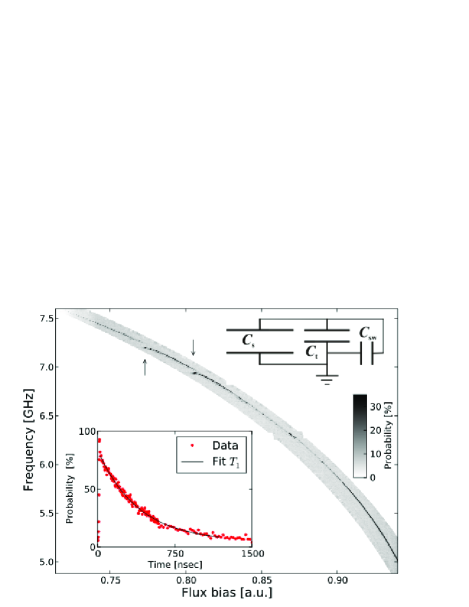
Qubit relaxation measurements via pulse excitation and time-varied delay before readout pulse were obtained when operated outside the avoided level structures. We measured a relaxation time of about , as shown in the lower inset of Fig. 3. This relaxation time is similar to that observed in the overlap qubits, which consistently have for - JJ size. Apart from the change to trilayer junctions, no modification from the previous design was made.
4 Loss estimation
| dielectric elements | capacitance | loss | |||
|---|---|---|---|---|---|
| ] | |||||
| shunt capacitor a-Si:H | 1250 | [15] | |||
| anodic side-wall oxide | 3.2 | [9] | |||
| tunnel barrier | 116 | [9] | |||
| measured |
We estimate the additional dielectric loss due to the sidewall oxide. The effective loss tangent of a parallel combination of capacitors is given by
with and being the real and imaginary part of the individual permittivity for capacitor with area and dielectric thickness .
Now, we discuss the individual loss contributions for all dielectrics. We design the qubit so that the dominant capacitance comes from the shunt capacitor made from a-Si:H, which has a relatively low loss tangent of . Including the non-negligible capacitance of the tunnel junction, this gives an effective loss tangent to the qubit of . Because the junction capacitance is about 10% of the shunting capacitance, the effective junction loss tangent is 10 times less than the loss tangent of the junction oxide. We statistically avoid the effects of two-level systems by purposely choosing to bias the devices away from the deleterious resonances. The loss tangent of the junction is smaller than the value for bulk aluminum oxide, approximately , and probably smaller than since long energy decay times () have been observed for an unshunted junction when operated away from resonances [9].
The anodic side-wall oxide contributes a small capacitance of about 3.2 fF, which can be calculated assuming a parallel plate geometry. Here, we use the dielectric constant for aluminum oxide, assume an area given by m, the width of the overlap, multiplied by m the thickness of the base layer, and estimate the thickness of the oxide nm as determined by the anodic process [11]. The anodic oxide is assumed to have a bulk loss tangent of [15], which gives a net qubit loss contribution of , about 5 times lower than for the a-Si:H capacitor. Note that we expect the loss from this capacitance to be even lower because of statistical avoidance of the TLS loss [9]. The small volume of the capacitor, equivalent to a volume tunnel junction, implies that most biases do not put the qubit on resonance with two-level systems in the anodic oxide.
5 Qubit lifetime and effective loss tangent
From the measured energy decay time , we determine the loss tangent of the qubit to be , using a qubit frequency . This is 3-5 times larger than our estimation of our dielectric losses, as shown in Table 1. We believe the qubit dissipation mechanism comes from some other energy loss sources as well, such as non-equilibrium quasiparticles [1].
6 Conclusion
In conclusion, we have shown that the use of a anodic oxide, self-aligned to the junction edge, does not degrade the coherence of present phase qubits [14]. We found performance comparable to the current generation of overlap phase qubits.
The new junction geometry may provide a method to integrate submicron sized, superior quality junctions (lower TLS densities) grown, for example, by MBE epitaxy to eliminate the need for shunt dielectrics. Also, our nanometer-thin, three dimensional-conform anodic passivation layer can be replaced by a self-aligned isolation dielectric at the side-wall, which could be used for all types of trilayer stacks.
Devices were made at the UCSB Nanofabrication Facility, a part of the NSF-funded National Nanotechnology Infrastructure Network.
The authors would like to thank D. Pappas for stimulating discussions. This work was supported by IARPA under grant W911NF-04-1-0204. M.W. acknowledges support from AvH foundation and M.M. from an Elings Postdoctoral Fellowship.
References
- [1] John M. Martinis, M. Ansmann, and J. Aumentado. Energy decay in superconducting josephson-junction qubits from nonequilibrium quasiparticle excitations. Phys. Rev. Lett., 103(9):097002, Aug 2009.
- [2] Matthias Steffen, M. Ansmann, R. McDermott, N. Katz, Radoslaw C. Bialczak, Erik Lucero, Matthew Neeley, E. M. Weig, A. N. Cleland, and John M. Martinis. State tomography of capacitively shunted phase qubits with high fidelity. Phys. Rev. Lett., 97(5):050502, Aug 2006.
- [3] Jeffrey S Kline, Haohua Wang, Seongshik Oh, John M Martinis, and David P Pappas. Josephson phase qubit circuit for the evaluation of advanced tunnel barrier materials. Supercond. Sci. Technol., 22(1):015004, 2009.
- [4] R. W. Simmonds, K. M. Lang, D. A. Hite, S. Nam, D. P. Pappas, and John M. Martinis. Decoherence in josephson phase qubits from junction resonators. Phys. Rev. Lett., 93(7):077003, Aug 2004.
- [5] A. Lupaşcu, P. Bertet, E. F. C. Driessen, C. J. P. M. Harmans, and J. E. Mooij. One- and two-photon spectroscopy of a flux qubit coupled to a microscopic defect. Phys. Rev. B, 80(17):172506, Nov 2009.
- [6] Jürgen Lisenfeld, Clemens Müller, Jared H. Cole, Pavel Bushev, Alexander Lukashenko, Alexander Shnirman, and Alexey V. Ustinov. Rabi spectroscopy of a qubit-fluctuator system. Phys. Rev. B, 81(10):100511, Mar 2010.
- [7] P. Bushev, C. Müller, J. Lisenfeld, J. H. Cole, A. Lukashenko, A. Shnirman, and A. V. Ustinov. Multiphoton spectroscopy of a hybrid quantum system. Phys. Rev. B, 82(13):134530, Oct 2010.
- [8] F. Deppe, M. Mariantoni, E. P. Menzel, S. Saito, K. Kakuyanagi, H. Tanaka, T. Meno, K. Semba, H. Takayanagi, and R. Gross. Phase coherent dynamics of a superconducting flux qubit with capacitive bias readout. Phys. Rev. B, 76(21):214503, Dec 2007.
- [9] John M. Martinis, K. B. Cooper, R. McDermott, Matthias Steffen, Markus Ansmann, K. D. Osborn, K. Cicak, Seongshik Oh, D. P. Pappas, R. W. Simmonds, and Clare C. Yu. Decoherence in josephson qubits from dielectric loss. Phys. Rev. Lett., 95(21):210503, Nov 2005.
- [10] A. Barone and G. Paterno. Physics and Applications of the Josephson Effect. John Wiley & Sons, 1982.
- [11] H. Kroger, L. N. Smith, and D. W. Jillie. Selective niobium anodization process for fabricating josephson tunnel-junctions. Appl. Phys. Lett., 39:280, 1981.
- [12] F. Müller, H. Schulze, R. Behr, J. Kohlmann, and J. Niemeyer. The Nb-Al technology at PTB: a common base for different types of Josephson voltage standards. Physica C, 354:66, 2001.
- [13] Matthew Neeley, M. Ansmann, Radoslaw C. Bialczak, M. Hofheinz, N. Katz, Erik Lucero, A. O’Connell, H. Wang, A. N. Cleland, and John M. Martinis. Transformed dissipation in superconducting quantum circuits. Phys. Rev. B, 77(18):180508, May 2008.
- [14] John M. Martinis. Superconducting phase qubits. Quantum Inf. Process., 8:81, 2009.
- [15] Aaron D. O’Connell, M. Ansmann, R. C. Bialczak, M. Hofheinz, N. Katz, Erik Lucero, C. McKenney, M. Neeley, H. Wang, E. M. Weig, A. N. Cleland, and J. M. Martinis. Microwave dielectric loss at single photon energies and millikelvin temperatures. Appl. Phys. Lett., 92(11):112903, 2008.
- [16] H. S. J. van der Zant, R. A. M. Receveur, T. P. Orlando, and A. W. Kleinsasser. One-dimensional parallel josephson-junction arrays as a tool for diagnostics. Appl. Phys. Lett., 65(16):2102–2104, 1994.