Low-velocity anisotropic Dirac fermions on the side surface of topological insulators
Abstract
We report anisotropic Dirac-cone surface bands on a side-surface geometry of the topological insulator Bi2Se3 revealed by first-principles density-functional calculations. We find that the electron velocity in the side-surface Dirac cone is anisotropically reduced from that in the (111)-surface Dirac cone, and the velocity is not in parallel with the wave vector k except for k in high-symmetry directions. The size of the electron spin depends on the direction of k due to anisotropic variation of the noncollinearity of the electron state. Low-energy effective Hamiltonian is proposed for side-surface Dirac fermions, and its implications are presented including refractive transport phenomena occurring at the edges of tological insulators where different surfaces meet.
pacs:
71.15.Mb, 73.20.-r, 73.61.Ng, 75.70.TjTopological insulators (TIs) are characterized by odd number of Dirac-cone-like surface bands which guarantees robust metallicity against arbitrary perturbations preserving time-reversal symmetry Fu (2); Moo , and by the helical spin texture of the surface states which leads to remarkable transport properties such as the absence of backscattering by non-magnetic defects as confirmed by experiments Rou ; T_Z ; Alp . The latter feature reminds us of graphene where charge carriers are also described as massless Dirac fermions, as demonstrated intriguingly by the Klein tunneling Kle (a) where normal incident wave exhibits perfect transmission through any finite potential barrier. A crucial difference is that TI involves real spins whereas graphene does pseudo-spins, so that, for example, one-dimensional wires of TI have maximum magnetoconductance at half integral flux quanta due to Berry phase acquired when circling around the wires Bar ; Vis .
Promising TI materials Zha ; Lin include series of rhombohedral materials Bi2Se3, Bi2Te3, and Sb2Te3 proposed by a recent first-principles calculation Zha , with the existence of single Dirac cone on their (111) surfaces indeed confirmed by angle-resolved photoemission spectroscopies Xia ; Hsi . Among them, Bi2Se3 is considered most promising in the application point of view due to its relatively large bulk band gap of 300 meV that can evade bulk conduction of thermally excited charge carriers at room temperature. This material has a layered structure where the Bi2Se3 quintuple layers (QLs) are stacked along the rhombohedral (111) direction Wyckoff combined by van der Waals type interaction. Thus, a natural cleaving face is the (111) surface between two QLs, and it has been the only surface considered theoretically or experimentally so far Song .
Surfaces other than the (111) surface, and interfaces between different surfaces, appear inevitably as step edges on cleaved (111) surfaces T_Z ; Alp ; Seo and as side surfaces in nanowires or nanoribbons Kon ; Cha ; Hon ; Pen . According to the topological band theory Fu (2); Moo , a strong TI like Bi2Se3 Zha should have odd number of Dirac cones on any arbitrary surface. However, existence of Dirac cones on a surface other than the (111) surface and their physical properties have never been studied by realistic electronic-structure calculations or by direct measurements.
In this Letter, we investigate the electronic structure of a side surface of Bi2Se3 using first-principles density-functional calculations, and find a Dirac-cone band structure, for the first time on a surface other than the (111) surface, consistently with the topological band theory. We find that the side-surface Dirac cone has lower symmetry, with elliptic equi-energy contour lines, and smaller velocity, introducing the refractive index in analogy with optics. We also present the low-energy Hamiltonian for the side-surface Dirac cone, and reflection and transmission properties at interfaces between different surfaces.

Our first-principles calculations are based on the density-functional theory with the generalized gradient approximation PBE and ab-initio norm-conserving pseudopotentials as implemented in SIESTA code SIE . We employ partial-core correction for Bi and Se pseudopotentials, pseudo-atomic orbitals (double--polarization basis set) for electronic wavefunctions, and a cutoff energy of 500 Ry for real-space mesh. We use a supercell containing a slab of Bi2Se3 and 9 Å thick vacuum to study surface states while preventing interaction between periodic images. Brillouin-zone (BZ) integration is performed with a two-dimensional (2D) 12 6 -point grid. Spin-orbit interaction is treated by relativistic pseudopotentials in the fully nonlocal form Kle (b). Atomic positions are taken from the experimental bulk structure Wyckoff .
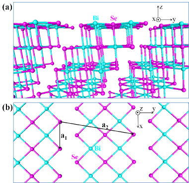
Figure 1 shows the atomic structure of the side surface considered in our present work. This side surface is stoichiometric in the sense that the topmost atomic layer of the surface and other atomic layers in parallel with it have stoichiometric Bi and Se compositions for Bi2Se3 within each atomic layer. The normal direction of the side surface is (221) in Miller indices of the rhombohedral bulk structure, making an angle of 58∘ to the (111) plane. In Fig. 1, no bond is drawn between Se atoms belonging to different QLs to represent the (111) cleaving planes with real-space gaps which are along the direction and repeated in the direction. The (221) surface has lower symmetry than the (111) surface, exhibiting anisotropy between and directions clearly. We construct a slab of eleven atomic layers of Bi2Se3 with the slab thickness of 30 Å to study surface electronic structures.

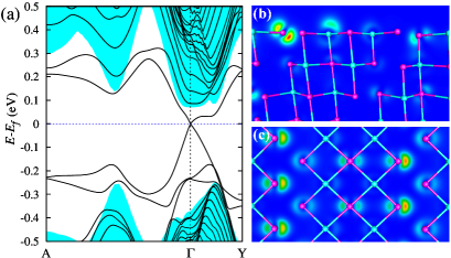
Figure 2(a) shows calculated electronic band structure along two lines in 2D BZ: from to and from to . Here, and are BZ boundaries along the reciprocal lattice vectors b1 and b2, respectively, associated with the real-space unit vectors a1 and a2 shown in Fig. 1(b). In Fig. 2(a), a crossing of linear bands is clearly visible at the point with the Dirac-point energy coinciding with the Fermi energy (). The bulk band continuum is projected onto the 2D surface BZ as filled areas in Fig. 2(a), where the bulk band gap is about 300 meV, consistently with previous calculation Zha . To check if the crossing bands are indeed surface states, we plot the squared amplitude of the wavefunction, , for a state at the point in Figs. 2(b) and (c). We find that it is mainly located on the surface atoms and decays rapidly into the bulk region, showing the surface-state nature of the crossing bands. Around the point in Fig. 2(a), we notice that the slope of the linear band is steeper, i.e. the Fermi velocity is larger, along the – direction than –, indicating anisotropy of the Dirac cone. Particle-hole asymmetry is also visible, where band linearity persists down to 200 meV below while the two bands bend significantly only 30 meV above .

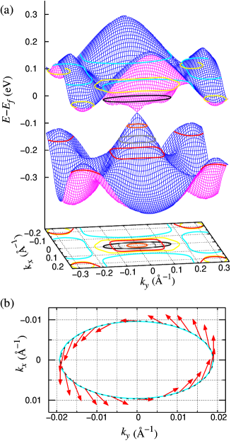
The shape of the side-surface Dirac cone is more obvious in the 2D plot of the bands near the point, as shown in Fig. 3(a). The Dirac cone is anisotropic, with the slope of the band and hence the Fermi velocity being larger in the direction than in the direction. As mentioned above, the linear band feature holds only within a very small energy window near , so the energy contours of 50 meV above (in black ) and below (in orange) look very different from each other [Fig. 3(a)]. At energies near close enough to ensure the band linearity, the energy contours are basically very close to ellipses.
We obtain the spin of a Dirac-cone state on the (221) surface by evaluating expectation values of the three spin-operator components, and the results are shown in Fig. 3(b). As expected for the helical spin fermion, the spin is almost perpendicular to the wave vector . Meanwhile, since each electronic state in this material is not a spin eigenstate but a noncollinear spin state due to the spin-orbit interaction, the spin size is not necessarily 1 in general Louie . Unlike the (111) surface where the spin size is independent of k, the spin size in the (221)-surface Dirac cone is found to depend on k, having its maximal value of 0.83 at and gradually decreasing toward 0.55 at around the Dirac cone [Fig. 3(b)].
Now we consider low-energy effective Hamiltonian similar to the previously suggested one Zha which basically corresponds to a Rashba-type surface spin-orbit Hamiltonian. Considering the reduced symmetry, the (221)-surface Hamiltonian in the first order of would be
| (1) |
where and are the Pauli matrices. The Fermi velocities and in and directions on the (221) surface are m/s and m/s, respectively, from our first-principles calculations. Energy eigenvalues are
| (2) |
and the corresponding eigenstates are
| (3) |
In Eqs. (2) and (3), the plus sign is for the conduction band while the minus sign is for the valence band. The equi-energy contour from Eq. (2) is an ellipse, which agrees with Fig. 3(b) at = 20 meV.
As mentioned earlier, interfaces of different surfaces are very often involved in many experimental situations where two different surfaces meet as a form of step edges on a cleaved TI surface or geometric edges in TI nanowires and nanoribbons. As our result shows that different TI surfaces have Dirac cones with different velocities, we can expect reflection and refraction behaviors in electronic transports at the interfaces of TI surfaces in close analogy with optics with distinct refractive-index materials. The concept of the refractive index can be introduced to a TI surface, and it provides a new insight for electronic transport in various TI geometries. We discuss two basic cases, a simple interface of TI surfaces and a Fabry-Perot interferometer.

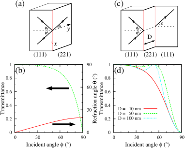
First we consider a simple interface between (111) and (221) surfaces which is parallel to the direction [Fig. 4(a)]. When a Dirac-cone state of the wave vector k is incident from the (111) surface to the interface at , with the incident angle , we can obtain the transmission probability and the refraction angle from the equality of -components of incident, reflected, and transmitted wave vectors, the energy conservation, and the continuity of the wave functions at the interface, similarly to the graphene case previously studied Net ; Kle (a); Par :
| (4) |
where appears from the relative phase of the two spinor components in Eq. (3). The refraction angle is given by , where and is the -component of the wave vector in the (221) surface region. The Fermi velocity in the (111) surface is about 5 105 m/s in our calculation, consistently with previous work Zha . Here we note that the incident and refraction angles satisfy the Snell’s law with the refractive index of the TI surfaces defined as the inverse of the phase velocity () of Dirac fermions, which, in general, depends on the k direction but not on the size of k.
Calculated transmission probability and refraction angle are plotted in Fig. 4(b) as functions of incident angle at = 20 meV. At normal incidence (), is 1, which means a perfect transmission, demonstrating the absence of back scattering due to the spin texture. As increases to 90∘, slowly decreases to 0, being greater than 0.5 for less than 80∘. At the same time, the refraction angle increases slowly from 0∘ and reaches 20∘ at . Thus, in the opposite situation in which the Dirac fermion is incident from the side surface to the (111) surface, the refraction angle reaches already at the incident angle of 20∘ and at larger incident angles the Dirac fermion cannot transmit through the interface. This implies that the total internal reflection can occur when the electron is incident from the side surface to the (111) surface, similarly to the optical system where the incident wave resides in a dielectric with higher refractive index than the other side of the interface. This opens a chance to produce evanescent waves of Dirac fermions on the (111) surface and their related phenomena.
Another relevant geometry is a Fabry-Perot interferometer where the (221) surface is made between two (111) surfaces [Fig. 4(c)], which might be a possible candidate to describe the step edges on the (111) surface in many previous experiments T_Z ; Alp . With boundary conditions similar to the above interface problem, we obtain reflectivity and hence the reflectance in analogy with the graphene case Kle (a)
| (5) |
where is the width of the (221) surface region [Fig. 4(c)], and the other parameters are defined similarly to the simple-interface case above.
The transmission probability through the interferometer, , is plotted as a function of the incident angle in Fig. 4(d), considering three different side-surface widths = 10, 50, and 100 nm, with = 20 meV. For all cases, we have the perfect transmission for the normal incidence () as in the simple-interface case, because of the forbidden back scattering. We also expect a perfect transmission to occur resonantly when the destructive interference happens between the incident and reflected waves, i.e., for positive integer from Eq. (5). Because of relatively low Fermi velocity in the side surface region, = 10 nm is not large enough for the resonant transmission to occur at = 20 meV, so monotonically decreases from 1 to 0 with increasing . For larger widths, 50 and 100 nm, reaches 1 at , where the resonance condition is fulfilled. In the case of = 100 nm, the resonance at is narrower, with less transmission at between 0∘ and 53∘.
Our Fabry-Perot structure can also be considered as an electronic analogy of the ‘optical fiber’ where propagating waves are confined within the high refractive index (low Fermi velocity) region by the total internal reflection. If the side surface region is clean enough to prevent the waves from escaping into the (111) surface region with high incident angles by defect scattering, this structure might be used as a one-dimensional conducting wire.
In conclusion, we performed first-principles calculations to investigate the electronic structure of a side surface of topological insulator Bi2Se3, finding a Dirac cone on the side surface, consistently with the topological-band-theory argument. The side-surface Dirac cone is found to be slow and anisotropic in an elliptic shape, with the spin size dependent on k. The low-energy effective Hamiltonian is proposed for the side-surface Dirac fermions, and the concept of the refractive index is introduced to the TI surface. Refraction, reflection, and transmission behaviors of Dirac fermions are demonstrated in the simple TI interface and the Fabry-Perot TI interferometer. Our idea of making TI junctions using different surfaces can be applied to form more complex structures such as superlattices, opening a chance for novel physical properties of Dirac fermions.
Acknowledgements.
We acknowledge helpful discussions with Jung Hoon Han and Young-Woo Son. This work was supported by NRF of Korea (Grant No. 2009-0081204) and KISTI Supercomputing Center (Project No. KSC-2008-S02-0004).References
- Fu (2) L. Fu, C. L. Kane, and E. J. Mele, Phys. Rev. Lett. 98, 106803 (2007).
- (2) J. E. Moore and L. Balents, Phys. Rev. B 75, 121306 (2007).
- (3) P. Roushan et al., Nature (London) 460, 1106 (2009).
- (4) T. Zhang et al., Phys. Rev. Lett. 103, 266803 (2009).
- (5) Z. Alpichshev et al., Phys. Rev. Lett. 104, 016401 (2010).
- Kle (a) M. I. Katsnelson, K. S. Novoselov, and A. K. Geim, Nature Phys. 2, 620 (2006).
- (7) J. H. Bardarson, P. W. Brouwer, and J. E. Moore, Phys. Rev. Lett. 105, 156803 (2010).
- (8) Y. Zhang and A. Vishwanath , Phys. Rev. Lett. 105, 206601 (2010).
- (9) H. Zhang et al., Nature Phys. 5, 438 (2009).
- (10) H. Lin et al., Nature Mater. 9, 546 (2010); H. Lin et al., Phys. Rev. Lett. 105, 036404 (2010).
- (11) Y. Xia et al., Nature Phys. 5, 398 (2009).
- (12) D. Hsieh et al., Phys. Rev. Lett. 103, 146401 (2009).
- (13) R. W. G. Wyckoff, Crystal Structures, Vol. 2. (John Wiley and Sons, New York, 1964).
- (14) J.-H. Song, H. Jin, and A. J. Freeman, Phys. Rev. Lett. 105, 096403 (2010).
- (15) J. Seo et al., Nature (London) 466, 343 (2010).
- (16) D. Kong et al., Nano Lett. 10, 329 (2010).
- (17) J. J. Cha et al., Nano Lett. 10, 1076 (2010).
- (18) S. S. Hong et al., Nano Lett. 10, 3118 (2010).
- (19) H. Peng et al., Nature Mater. 9, 225 (2010).
- (20) J. P. Perdew, K. Burke, and M. Ernzerhof, Phys. Rev. Lett. 77, 3865 (1996).
- (21) D. Sanchez-Portal, P. Ordejon, E. Artacho, and J. M. Soler, Int. J. Quantum Chem. 65, 453 (1997).
- Kle (b) L. Kleinman and D. M. Bylander, Phys. Rev. Lett. 48, 1425 (1982).
- (23) C. L. Kane and E. J. Mele, Phys. Rev. Lett. 95, 146802 (2005); O. V. Yazyev, J. E. Moore, and S. G. Louie, ibid. 105, 266806 (2010).
- (24) A. H. Castro Neto et al., Rev. Mod. Phys. 81, 109 (2009).
- (25) C.-H. Park et al., Nano Lett. 8, 2920 (2008).