Interference of surface plasmon polaritons from a ”point” source
Abstract
The interference patterns of the surface plasmon polaritons(SPPs) on the metal surface from a ”point” source are observed. These interference patterns come from the forward SPPs and the reflected one from the obstacles, such as straightedge, corner, and ring groove structure. Innovation to the previous works, a ”point” SPPs source with diameter of nm is generated at the freely chosen positions on Au/air interface using near field excitation method. Such a ”point” source provides good enough coherence to generate obvious interference phenomenon. The constructive and destructive interference patterns of the SPPs agree well with the numerical caculation. This ”point” SPPs source may be useful in the investigation of plasmonics for its high coherence, deterministic position and minimum requirement for the initial light source.
I Introduction
Surface plasmon polaritons (SPPs), collective oscillating electrons excited by electromagnetic field, have been studied for decades and a great of interest has been injected into this area. Such SPPs are involved in a wide range of phenomena Barnes03 ; Ozbay06 , including nanoscale optical waveguiding Bozhevolnyi06 ; Takahara97 ; Takahara04 ; Zia06 , perfect lensing Pendry00 , extraordinary optical transmission Ebbesen98 , subwavelength lithography Fang05 , and ultrahigh sensitivity biosensing Liedberg83 . It has also been experimentally proved that SPPs are useful in the investigation of quantum information Altewischer02 ; Fasel05 ; Ren06 . To realize the full potential technology of plasmonics, we need to construct a general framework to describe the propagation, diffraction, and interference of SPPs. The interference phenomenon of SPPs has been studied in many works Lezec06 ; Lopez07 ; Paci07 ; Zia07 ; Ren08 , for example, a double-slit experiment with SPPs is presented, which reveals the analog between SPPs propagating along the surface of metallic structures and light propagating in conventional dielectric components Zia07 .
In the investigation of plasmonics, a good source of SPPs is very important which proposes high demands on the exciting light source. Usually the SPPs are excited by far-field excitation using grating coupling or attenuated total reflection (ATR). The spots of the focused light always have the diameter bigger than half of the light wavelength due to diffraction limit. As we know, one of the most important properties of light source is the coherence, which is essential in the study of the interference. For a non-point source, the spatial coherence is correlated with the size of source, such as the case in the double-slit interference experiment. Another standing problem for the SPPs source is the precisely generation of SPPs at designated positions of nanostructuresDall09 ; Bouhelier07 , which is very important in usage of plasmonic devices. In this paper, a ”point” SPPs source is generated by a near-field scanning optical microscope (NSOM) probe with a diameter of few hundred nanometers, which is smaller than the wavelength of SPPs. With the benefit of the near field scanning method, the source can also be placed at any positions of the nanostructure precisely. The interference patterns between the forward SPPs and the reflected one from the obstacles, such as straightedge, corner, and ring groove structure are detected by another NSOM probe connected to an avalanche photo diode (APD). The ”point” SPPs source makes the interference pattern clear due to its small size. This new method will benefit the study of the plasmoincs where a SPPs source with high coherence and deterministic position is needed. Since the SPPs only propagate on the surface, the same as the wave on the water surface, our results may also be useful in the investigation of some fundamental physics by simplifying the model from three dimensional space to two dimensional space.
II Results and discussion
In this literature, the intensity distribution of SPPs is studied by the near-field optical measurements with scanning dual probe microscope/NSOM system (Nanonics Imaging Ltd., Jerusalem, Israel). This system allows for simultaneous atomic force microscopy (AFM) and NSOM imaging. A sketch map of our experimental setup is given in Figure 1. The SPPs is generated by a cantilevered aperture NSOM probe (diameter 100 nm or 500 nm), which is connected with a semiconductor laser with 670 nm wavelength using a single mode polarization maintaining fiber. The NSOM probe is coated with Cr-Au(0.02 and ) to prevent light emitting from the side of the fiber cone and concentrate light to emit from the aperture. When the probe approaches the metal surface with the distance of only a few nanometers (called near field), the SPPs can be excited effectivelyDall09 . This makes the light source small enough to be a ”point” source which avoids the shortcomings that light diffract from the fiber cone with a big scatting spot Bouhelier07 . A similar 100 nm width aperture NSOM probe scan the sample in collection mode to measure the field intensity associated with the interference pattern of the propagating SPPs waves. It is finally collected by a single photon detector (SPCM-15, PerkinElmer Optoelectronics, Canada). The metal plate used in our experiment to excite SPPs is produced as follows. After subsequently evaporating a 3-nm titanium bonding layer, a thick gold layer is evaporated onto a 0.5-mm-thick silica glass substrate. An initial AFM scan of the sample was performed, which gave a root mean squared roughness of 2 nm. The gold layer is thick enough to avoid the excitation of SPPs on the interface of .
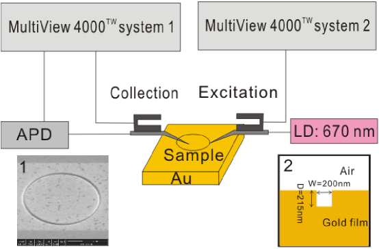
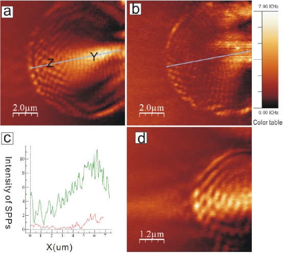
Firstly, we discuss the relation between the visibility of interference patterns and the size of the ”point” source. According to the coherence theory, the better the coherence condition is met, the higher visibility of the interference fringes can be achieved. We test this by observing the SPPs interference phenomenon of a ring structure with different ”point” sources size. The ring-shaped groove structure is produced with focused ion beam etching system (DB235 of FEB Co.), which has a groove depth of 215 nm, width of 200 nm and diameter of (see inset of Figure 1). The SPPs is excited by the laser light of 670 nm wavelength through the excitation NSOM probe and another NSOM probe with diameter of nm works on the collection mode to scan the sample and image the SPPs distribution on the metal surface. When the excitation probe approaches the metal plate, the excited SPPs propagate along the interface of the Au/air and strike the ring edge. According to the Huygens’ principle, every point of the groove’s edge can be regarded as a new ”point” SPPs source, from which the SPPs form the interference pattern in the observed area. Two excitation NSOM probes with aperture diameters 100 nm and 500 nm are used and the NSOM images are given in Figure 2a and 2b respectively. The interference pattern in Figure 2a is much clearer than that in Figure 2b which confirms that a NSOM probe with smaller aperture produces a higher coherent SPPs source. Figure 2c gives the SPPs intensity distribution along the blue line in Figure 2a and 2b, which also shows an obvious difference between the two cases. For a further study, we also change the diameter of the ring to with the same excitation probe of nm diameter. The NSOM image of the SPPs distribution is given in Figure 2d which possesses the same interference pattern but less clear. Since the probe with diameter can act as a better ”point” SPPs source, we use it to observe the interference patterns of SPPs in the following experiments.
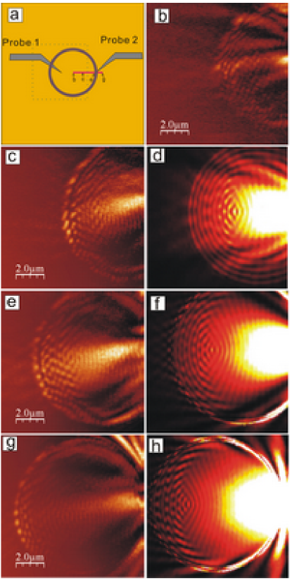
Besides the small size of the SPPs source, another benefit of our method is the deterministic source position. We can move the excitation probe to any positions of the sample by performing an initial AFM scan. This is illustrated by observing the interference phenomenon of the ring structure with different SPPs source positions, as shown in Figure 3a. The SPPs is excited at the positions of ”b”, ”c”, ”e” and ”g” along the red line, where ”b” is the center of the ring, ”c” and g are inner and out of the ring structure and ”e” is inside the ring groove. Another NSOM probe works on the collection mode to scan the area marked by dished square and image the SPPs distribution on the sample surface. The interference pattern changes with different excitation positions as shown in Figure 3b, c, e and g accordingly. A simple description is given as follows. When the excitation probe is put at the center of the ring structure (position ”b”), the distance between the point source and the ring structure is almost the same. A ring shaped interference patterns are observed as shown in Figure 3b. The inhomogeneity may come from the imperfect NSOM probe. This is verified by scanning a flat metal surface near the excitation probe (see the supporting information), which also give a similar asymmetric energy distribution. This ring shaped interference patterns change to curves when SPPs are generated at ”c”. When the excitation probe move to position ”g”, only the right part of the groove acts as new SPPs sources. The SPPs generated at the groove edge propagate from right to left as shown in Figure 3g. At the right part inside the ring, the fringe is curved since the wall of the groove is curved. While at the left part, especially nearby the groove, the interference pattern looks like grid, which is formed by the interference of the forward SPPs and the reflected ones from the left groove. More interestingly, the image is much clear when the excitation probe is put inside the groove as shown in Figure 3e. At this time, guiding SPPs are excited in the groove and transmit along the groove waveguideBozhevolnyi06 . The leakage parts from the groove edge act as new sources. Obviously, the intensities of these new sources are much higher than the cases that excitation probe is outside the groove. This gives a brighter interference pattern. Besides the interference patters of the SPPs, an intensity peak appears at the center of the ring, because of the SPPs focusing effect of the ring-shaped grooveLiu05 . Numerical calculations are also given for the cases that excitation probe is put the positions ”c”,”e” and ”g”, as shown in Figure 3d, f and h. They are similar with the experimental results.
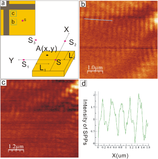
To give a more clear picture of this interference phenomenon, we also use more simple metal structures, for example, a straight edge and a corner. We cut two cross slots on the gold film with the width of , which is big enough to stop the SPPs coupling between two edges of the slot. The sample is excited at point S, as shown in inset of Figure 4a. Another NSOM probe (collection probe) scans the area of marked by ”b”. The positions of the two probes and the distance between them can be controlled freely by the two SPM controllers of the system. The SNOM image is shown in Figure 4b and the fringe is formed by the interference of the propagating SPPs and the reflected one from the vertical edge of the gold film, since the SPPs reflected from the farther horizontal edge can be neglected at this area. Figure 4d is the SPPs intensity distribution along the blue line in Figure 4b, which shows that the average period of the stripes is about 320 nm. This is half of the wavelength of the SPPs, which is 640 nm calculated from the function of
| (1) |
where and are the wavelength of the SPPs and the light in vacuum, and are the real parts of the metal and dielectric permittivities, respectively. Next, the collection probe 2 scans the area of marked by ”c” with the excitation probe at position S as former. The SNOM image is shown in Figure 4c, in which we can see grids obviously. In this case, the distances between the scanned area and the two edges are about the same, so the SPPs waves reflected from the horizontal edge must also be considered. To give a simple description, we establish a two-dimensional coordinate system with the excitation position S as the origin on the surface of Au film as shown in Figure 4a. At an arbitrary point , if we only consider the impact of the edge along the direction, the interference comes from the two SPPs waves from the point S and its symmetric point with the vertical edge. Obviously, the interference fringes should be parallel to the edge approximately and the period is given by . Now, plus the impact of another adjacent edge, there are four symmetric point sources with the two cross edges, S, , and as shown in Figure 4a. The total electric field at point A is
| (2) |
where , , and are the electric field of SPPs waves at point A from ”point” sources of S, , and respectively. This interference pattern is more complex than the case only considering the superposition of two waves. But in principle, the interference pattern should be grid in the area where the SPPs source from four sources have to be considered simultaneously.
III Conclusion
In this literature, a ”point” source is used to study the interference of the SPPs. The interference patterns of strip, grid and ring are observed on the metal surface. The interference pattern appears more clear when the coherence condition is met better by using a smaller SPPs source size. The success of the experiment is benefited from the use of the NSOM probe to excite the sample in the near field. This ”point” SPPs source can be used in many areas for its high coherence, deterministic position and minimum requirement for the initial light source.
III.1 Methods
Preparation of Samples. The metal plate is prepared by subsequently evaporating a 3-nm titanium bonding layer and a gold layer onto a 0.5-mm-thick silica glass substrate. We cut two cross slots on the gold film with a width of about by the tip of a knife and then the corner and edges are formed. The ring shaped groove with depth of 215 nm, width of 200 nm and diameter of was produced with focused ion beam etching system (DB235 of FEB Co.).
SPPs Excitation and Detection. A semiconductor laser of 670 nm wavelength is connected to the cantilevered NSOM probe by a single mode polarization maintaining fiber. The polarization of the laser is controlled by a polarizer. The metal sample of two cross slots is excited at the point S by the excitation NSOM probe. The other similar NSOM probe with a 100 nm width aperture scans the areas of marked by ”b” and by ”c” respectively in collection mode and measures the field intensity associated with the interference pattern of the propagating SPPs waves. The position of the two probes and the distance between thems are controlled by the two SPM controllers of the system. The collection NSOM probe is connected to a single photon detector (SPCM-15, PerkinElmer Optoelectronics, Canada) through another single mode polarization maintaining fiber. For case of the ring groove structure with a diameter of , the experimental setup is the same as the former. The excited points change along the red line in Figure 3a and the collection probe scans the left part of the ring each time. We also scan a ring groove structure with a diameter of using the same method.
This work was funded by the National Basic Research Programme of China (Grants No.2011CBA00200), the Innovation funds from Chinese Academy of Sciences, and the National Natural Science Foundation of China (Grants No.10874163 and No.10904137),Anhui Provincial Natural Science Foundation(Grants No. 090412053) and Science and Technological Fund of Anhui Province for Outstanding Youth(Grants No.2009SQRZ001ZD).
Figure S1 show the NSOM image of the SPPs distribution on the gold plane near the point SPPs source without obstacles; Figure S2 show the NSOM images of the SPPs distribution on the the ring groove structure with a diameter of excited by the 670 nm and 633 nm wavelength laser respectively.
References
- (1) Barnes, W. L.; Dereux, A.; Ebbesen, T. W., Surface plasmon subwavelength optics. Nature 2003, 424 (6950), 824-830.
- (2) Ozbay, E., Plasmonics: Merging Photonics and Electronics at Nanoscale Dimensions. Science 2006, 311 (5758), 189-193.
- (3) Bozhevolnyi, S. I.; Volkov, V. S.; Devaux, E.; Laluet, J.-Y.; Ebbesen, T. W., Channel plasmon subwavelength waveguide components including interferometers and ring resonators. Nature 2006, 440 (7083), 508-511.
- (4) Takahara, J.; Yamagishi, S.; Taki, H.; Morimoto, A.; Kobayashi, T., Guiding of a one-dimensional optical beam with nanometer diameter. Opt. Lett. 1997, 22 (7), 475-477.
- (5) Takahara, J.; Kobayashi, T., Low-Dimensional Optical Waves And Nano-Optical Circuits. Opt. Photon. News 2004, 15 (10), 54-59.
- (6) Zia, R.; Schuller, J. A.; Chandran, A.; Brongersma, M. L., Plasmonics: the next chip-scale technology. Materials Today 2006, 9 (7-8), 20-27.
- (7) Pendry, J. B., Negative Refraction Makes a Perfect Lens. Phys. Rev. Lett. 2000, 85 (18), 3966.
- (8) Ebbesen, T. W.; Lezec, H. J.; Ghaemi, H. F.; Thio, T.; Wolff, P. A., Extraordinary optical transmission through sub-wavelength hole arrays. Nature 1998, 391 (6668), 667-669.
- (9) Fang, N.; Lee, H.; Sun, C.; Zhang, X., Sub-Diffraction-Limited Optical Imaging with a Silver Superlens. Science 2005, 308 (5721), 534-537.
- (10) Liedberg, B.; Nylander, C.; Lunstr?m, I., Surface plasmon resonance for gas detection and biosensing. Sensors and Actuators 1983, 4, 299-304.
- (11) Altewischer, E.; van Exter, M. P.; Woerdman, J. P., Plasmon-assisted transmission of entangled photons. Nature 2002, 418 (6895), 304-306.
- (12) Fasel, S.; Robin, F.; Moreno, E.; Erni, D.; Gisin, N.; Zbinden, H., Energy-Time Entanglement Preservation in Plasmon-Assisted Light Transmission. Phys. Rev. Lett. 2005, 94 (11), 110501.
- (13) Ren, X. F.; et al., Plasmon-assisted transmission of high-dimensional orbital angular-momentum entangled state. EPL (Europhysics Letters) 2006, 76 (5), 753.
- (14) Gay, G.; Alloschery, O.; Viaris de Lesegno, B.; O/’Dwyer, C.; Weiner, J.; Lezec, H. J., The optical response of nanostructured surfaces and the composite diffracted evanescent wave model. Nat Phys 2006, 2 (4), 262-267.
- (15) Lopez-Tejeira, F.; Rodrigo, S. G.; Martin-Moreno, L.; Garcia-Vidal, F. J.; Devaux, E.; Ebbesen, T. W.; Krenn, J. R.; Radko, I. P.; Bozhevolnyi, S. I.; Gonzalez, M. U.; Weeber, J. C.; Dereux, A., Efficient unidirectional nanoslit couplers for surface plasmons. Nat Phys 2007, 3 (5), 324-328. Dereux, Nature Phys. 3, 324 (2007).
- (16) Pacifici, D.; Lezec, H. J.; Atwater, H. A., All-optical modulation by plasmonic excitation of CdSe quantum dots. Nat Photon 2007, 1 (7), 402-406.
- (17) Zia, R.; Brongersma, M. L., Surface plasmon polariton analogue to Young’s double-slit experiment. Nat Nano 2007, 2 (7), 426-429.
- (18) Ren, X.-F.; Guo, G.-P.; Huang, Y.-F.; Wang, Z.-W.; Zhang, P.; Guo, G.-C., Interference of surface plasmon polaritons controlled by the phase of incident light. Appl. Phys. Lett. 2008, 92 (17), 171106-3.
- (19) Dallapiccola, R.; Dubois, C.; Gopinath, A.; Stellacci, F.; Dal Negro, L., Near-field excitation and near-field detection of propagating surface plasmon polaritons on Au waveguide structures, Appl.Phys.Lett. 2009, 94, 243118.
- (20) Bouhelier, A.; Ignatovich, F.; Bruyant, A.; Huang, C.; Colas des Francs, G.; Weeber, J. C.; Dereux, A.; Wiederrecht, G. P.; Novotny, L., Surface plasmon interference excited by tightly focused laser beams. Opt. Lett. 2007, 32 (17), 2535-2537.
- (21) Liu, Z.; Steele, J. M.; Srituravanich, W.; Pikus, Y.; Sun, C.; Zhang, X., Focusing Surface Plasmons with a Plasmonic Lens. Nano Letters 2005, 5 (9), 1726-1729.