Abstract
In this work we show theoretically that it is possible to design a large band gap in the infrared range using a one-dimensional Photonic Crystal heterostructure made of porous silicon. Stacking together multiple photonic crystal substructures of the same contrast index , but of different lattice periods, it is possible to broad the narrow forbidden band gap that can be reached by the low contrast index of the porous silicon multilayers. The main idea in this work is that we can construct a Giant Photonic Band Gap -as large as desired- by combining a tandem of photonic crystals substructures by using a simple analytical rule to determine the period of each substructure.
Large Frequency Range of Photonic Band Gaps on Porous
Silicon Heterostructures for Infrared Applications
J. Manzanares-Martinez and P. Castro-Garay
Centro de Investigacion en Fisica de la Universidad de Sonora,
Apartado Postal 5-088, Hermosillo, Sonora 83190, Mexico.
R. Archuleta-Garcia and D. Moctezuma-Enriquez
Programa de Posgrado en Ciencias (Fisica) de la Universidad de Sonora,
Calle Rosales y Boulevard Luis Encinas, Hermosillo, Sonora, Mexico.
Keywords: Photonic Crystals, Infrared, Porous Silicon
1 Introduction
In recent years, there has been much interest in the fabrication and study of Photonic Crystals (PCs) [1, 2] which are periodic dielectric composites with a periodicity matching the wavelength of electromagnetic waves in the visible or infrared range. [3, 4, 5] The spatial modulation of the refractive index leads to Photonic Band Gaps (PBG) where the electromagnetic fields cannot propagate due to the destructive interference. The absence of electromagnetic states in the PBG allow the possibility that the PCs can be perfect mirrors for light impinging from any direction or polarization. [6] These PC-based mirrors have low losses as compared with old metallic mirrors, specially in the infrared range. [7]
Theoretical photonic band structure calculations predict complete band gaps for a number of periodic dielectric lattices in two (2D) or three (3D) dimensions. [8] Nevertheless, to fabricate 3D PCs with a band gap in the infrared is a difficult and time consuming task. [9] Additionally, even with the most recent experimental techniques it has only been possible to fabricate 3D structures with a low variation in the refractive index, typically .[7] This low index contrast attained in 3D PCs is a limiting factor in some applications in telecoms or near infrared range where a large range of band gap is required. [10, 11] To obtain wider PBG it is desirable to increase the refractive index, different authors have reported that the width of the band gap is a function of the contrast index, the larger the better. [12, 13, 14]
Recently several improvements in the fabrication of one-dimensional (1D) photonic crystals or multilayers based in porous silicon have been reported. [15, 16] Porous silicon fabrication techniques are flexible, cheap and feasible to grow with a high number of periods in the infrared range.[17, 18] Porous silicon multilayers have a low index contrast, however. [7] Nevertheless, it has been reported that the band gap can be enlarged by using heterostructures. [19] A heterostructure is a mirror composed by a tandem of PC substructures or submirrors and the idea is to add the band gaps of each submirror. [20] Some of the present authors have previously reported the design of a heterostructure mirror in the complete visible.[21] In this work, we present the design of a photonic heterostructure mirror in the near infrared range ( - ). Our theoretical approach shows that it is possible to obtain a near infrared mirror with fewer layers than those needed in an already published work, [15] where the heterostructure mirror was designed following an experimental rule. [17]
2 Theory
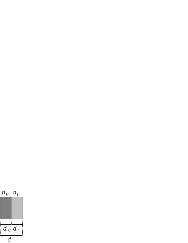
Let us first consider a PC made by the infinite periodic repetition of the unit cell illustrated in Fig. 1. The unit cell is composed by two materials, one is of high () and the other of low () refractive index. The width of each layer is and , respectively. The unit cell have a width of . The Photonic Band Structure is obtained using an analytical formula derived by Yeh et al. [22]
| (1) |
, and are the wavevector, frequency and speed of light, respectively. It is convenient to write this equation in the form
| (2) |
where we have introduced the filling fraction as the space occuped by each material in the unit cell, and . The reduced frequency is
| (3) |
where we have considered that and .
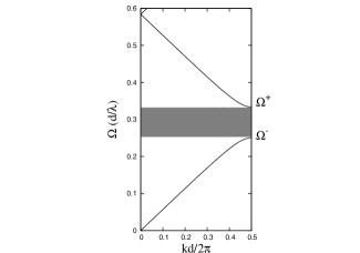
We consider a unit cell composed by two high and low typical porous silicon refractive indices values, and . The filling fractions that optimizes the width of the first photonic band gap are calculated by using the quarter wave condition , [23] obtaining and , respectively. In Fig. 2 we present the photonic band structure. The gray zone is the first forbidden band gap which is limited by an upper and lower reduced frequency with values and , respectively. These limits can be related to the wavelength by using eq. (3)
| (4) |
| (5) |
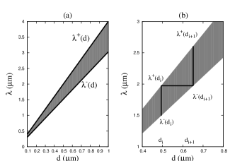
In Fig. 3(a) we plot in the gray zone the enlargement of the band gap as a function of the period, . The upper and lower limits of the band gap are and , respectively. To design a heterostructure with a giant band gap, we stack together PC lattices or submirrors of different periods such that the band gaps can be added. In panel (b) we illustrate the addition of the band gaps of two lattices of periods and . The submirror of period () has upper and lower limits of () and (), respectively. The purpose is to choose the periods so that the upper limit of one submirror is equal to the lower limit of the next submirror, as follows
| (6) |
Using eqs. (4), (5) and (7) this relation can be written as a rule for the periods in the form
| (7) |
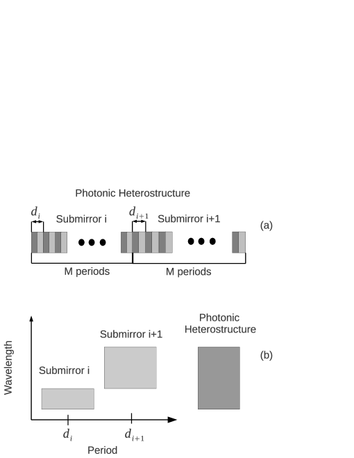
Fig. 4 presents in panel (a) a PC heterostructure formed by two submirros with a lattice period of and , respectively. Each submirror has unit cell periods. In panel (b) we illustrate the addition of the photonic band gap of each submirror to make a wider heterostructure band gap.
3 Numerical results
In order to present our method to design a photonic crystal heterostructure with an enlarged band gap we consider the case of a mirror for the whole near infrared range, specifically with a low and high frequency limits of and , respectively. To select the thickness of the first submirror , we consider that its lower frequency limit is equal to the low frequency limit of the heterostructure mirror, . This condition can be written in the form
| (8) |
The first submirror period is obtained using the relation
| (9) |
To determine the following submirror periods () we use eq. (7). For each submirror, the high and low frequency limits are calculated using eqs. (4) and (5). The idea is to calculate the period and the frequency limits for submirrors until a condition is reached where the high frequency limit of the submirror is greater than the high frequency limit of the desired heterostructure mirror ,
| (10) |
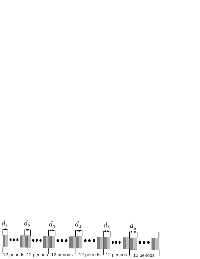
For the case of the porous silicon PC calculated in the previous section, we have found that with 6 submirrors can cover the whole near infrared range. In table 1 we present the periods and band gaps limits calculated for each submirror. Fig. 5 shows a schematic of the photonic crystal heterostructure composed by six submirros, where each submirror posses 12 unit cells periods. The complete heterostructure has 72 unit cells. In Fig. 6 we present the calculated light reflection of the photonic heterostructure. The simulation program used is based on the transfer matrix method [22]. We observe that total reflection occurs in the range -.
| submirror | (m) | (m) | (m) |
|---|---|---|---|
| 1 | 0.21 | 0.85 | 0.65 |
| 2 | 0.28 | 1.13 | 0.85 |
| 3 | 0.37 | 1.49 | 1.13 |
| 4 | 0.49 | 1.97 | 1.49 |
| 5 | 0.65 | 2.60 | 1.97 |
| 6 | 0.86 | 3.43 | 2.60 |

4 Discussion
We have demonstrated that a porous silicon heterostructure reflector with low refractive contrast index can be designed by using a simple rule to determine the periods. The near infrared reflector consists of 6 submirrors with 12 unit cells periods each. The complete structure has 72 unit cells and reflects light in the infrared range of -. In comparison, in Ref. [15] it has been reported the fabrication of a heterostructure mirror for the near infrared range which is composed by 45 submirrors of 4 periods for each submirror, obtaining a total of 180 unit cells. The heterostructure that we have designed in section III has fewer layers as compared to Ref. [15]. On the other hand, our formula to determine the submirror periods is based on a clear physical insight related to the addition of the photonic band gaps, while it is not clear the reason why the empirical rule proposed Refs. [15, 17] should work.
5 Conclusion
We have presented a simple strategy to design a heterostructure mirror composed by a stack of several submirrors with the same refractive indices and and different period thicknesses . Stacking together different substructures the band gap of the heterostructure is the union of the band gap of the submirrors. For this reason, each submirror has been chosen so that the band gaps can be added. We have presented the design of a mirror for the near infrared range. However, our method can be used to design a heterostructure with a band gap as large as wide which can work in any frequency range as far as the refractive indices of the composite materials remains valid.
The proposed porous silicon based photonic heterostructure has been designed using parameters of refractive indices and periods that are compatible with the well established porous silicon technology. These structures have an excellent potential for integration with optoelectronic technology. This is relevant because one of the goals of silicon based fabrication techniques is to integrate infrared or optical components such as modulators, photodetectors or sensors in porous silicon ships to fabricate new photonic devices.
ACKNOWLEDGEMENTS. PCG thanks the Optical Academy of the Department for Physics Research of the Sonora University for a temporary contract as Research Associate. RAG acknowledges a grant provided by the CONACYT project CB-2008-104151. We thank the head of our Department for Physics Research, Prof. Julio Saucedo Morales for reading the manuscript.
References
- [1] E. Yablonovitch, Phys. Rev. Lett., 58, 2059 (1987).
- [2] S. John, Phys. Rev. Lett., 58, 2486 (1987).
- [3] T. F. Krauss, R. M. de la Rue, S. Brand, Nature, 383, 699 (1996).
- [4] C. C. Chung, V. Arbet-Engels, A. Scherer, and E. Yablonovitch, Physica Scripta, 68, 17 (1996).
- [5] S. Y. Lin, J. G. Fleming, D. L. Hetherington, B. K. Smith, R. Biswas, K. M. Ho, M. M. Sigalas, W. Zubrzycki, S. R. Kurtz, and J. Bur, Nature, 394, 251 (1998).
- [6] J. N. Winn, Y. Fink, S. Fan, and J. D. Joannopoulous, Opt. Lett. 23, 1573 (1998).
- [7] T. Zhai, D. Liu, X. Zhang, Front Phys. China, 5, 266 (2010).
- [8] J. D. Joannopoulos, R. D. Meade, and J. N. Winn, Photonic Crystals, Princeton University Press, Princeton (1995).
- [9] Y. L. Lai, and C. C. Chiu, Colloids and Surfaces A: Physicochemical and Engineering Aspects, 313, 497 (2008).
- [10] S. S. Dhillon, C. Sirtori, S. Barbieri, A. de Rossi, M. Calligaro, H. E. Beere, and D. A. Ritchie, Appl. Phys. Lett., 87, 071101 (2005).
- [11] S. Zlatanovic1, J. S. Park, S. Moro, J. M. Chavez-Boggio, I. B. Divliansky, N. Alic, S. Mookherjea, and S. Radic, Nature Photonics, 4, 561 (2010)
- [12] E. Yablonovitch, Science, 289,557 (2000).
- [13] J. Wijnhoven, and W. L. Vos, Nature, 281, 802 (1998).
- [14] T. Y. M. Chan, O. Toader, and S. John, Phys. Rev. E, 71, 46605 (2005).
- [15] V. Agarwal and J. A. del Rio, Int. J. of Mod. Phys. B 20, 99 (2006)
- [16] A. G. Palestino, M. B. de la Mora, J. A. del Rio, C. Gergely, E. Perez, Appl. Phys. Lett., 91, 121909 (2007).
- [17] V. Agarwal and J. A. del Rio, Appl. Phys. Lett. 82, 1512 (2003).
- [18] Z. Wang, J. Zhang, S. Xu, L. Wang, Z. Cao, P. Zhan and Z. Wang, J. Phys. D: Appl. Phys, 40, 4482-4484 (2007).
- [19] J. Zi, J. Wan, and C. Zhang, Appl. Phys. Lett. 73 2084-2086 (1998).
- [20] E. Istrate, and E. H. Sargent, Rev. Mod. Phys. 78, 455 (2006).
- [21] R. Archuleta-Garcia, D.Moctezuma-Enriquez, J. Manzanares-Martinez, Journal of Electromagnetics Waves and Applications, 24,351 (2010).
- [22] Pochi Yeh, Optical Waves in Layered Media, Wiley, New York (1998).
- [23] H. S. Sozuer, and K. Sevim, Phys. Rev. B, 72, 195101 (2005).
Received: Month xx, 200x