A SIMPLE CIRCUIT WITH DYNAMIC LOGIC ARCHITECTURE OF BASIC LOGIC GATES
We report experimental results obtained with a circuit possessing
dynamic logic architecture based on one of the theoretical schemes proposed by H. Peng and collaborators in 2008.
The schematic diagram of the electronic circuit and its implementation to
get different basic logic gates are displayed and discussed. In particular, we show explicitly how to get the electronic NOR, NAND, and XOR gates. The proposed electronic circuit is easy to build because it employs only resistors, operational amplifiers and comparators.
Keywords: chaos computing, analog electronic, piecewise-linear functions.
Dynamic-logic4.tex Int. J. Bif. Chaos 20(8) 2547-2551 (2010)
1. Introduction
There is great interest in developing new working paradigms in order to complement and even replace the present statically-wired computer architectures. One of the frontier ideas put forth by Sinha and Ditto in 1998 [Sinha & Ditto, 1998] is to get new devices with a dynamic logic architecture that now is called chaos computing because chaotic (non-linear) elements are employed to get the logic operations [Sinha & Ditto, 1999; Kuo, 2005; Munakata et al., 2002]. The main task in this case is to achieve logic gates (also called cells here) that are able to change their response according to the control parameter and reconfiguring the device in order to obtain whatever logic gate. These dynamic logic gates give us the possibility to build logic chips for the next generation of computers. Moreover, Sinha and Ditto [Sinha & Ditto, 1999] extended their proposal to encode numbers, perform specific arithmetic operations such as addition and multiplication, and so on. In a theoretical work of Kuo [Kuo, 2005] the logistic map was used as the chaotic element and employed to emulate logic gates. Currently, there is stimulating research activity in exploiting the logic features of the nonlinear dynamical systems through their electronic implementations [Murali et al., 2009; Murali et al., 2009; Murali et al., 2005; Murali et al., 2003].
The goal of this work is to present some experimental results that we obtained by means of a simple electronic circuit
with dynamic logic architecture. The circuit was designed based on the first of the three theoretical schemes reported by Peng and collaborators in
order to build dynamic logic gates [Peng et al., 2008]. The electric diagram of that scheme is easy to implement in our
electronic circuit and the employed components can be acquired in any electronic store.
2. Electronic Dynamical Logic Gate
The discrete dynamical system used in [Peng et al., 2008] to simulate dynamic logic gates is the following:
| (1) |
where and are positive constants, is the bifurcation parameter which acts as the logic-gate controller, is the number of iterative steps, and are the input logic signals, and is the output signal.
The dynamic logic gate given by equation (1) is controlled through the parameter according to the intervals given in table 1 and restricted to , , see [Peng et al., 2008].
| When K : | The cell is: |
|---|---|
| NOR | |
| NAND | |
| XOR | |
| OR | |
| AND |
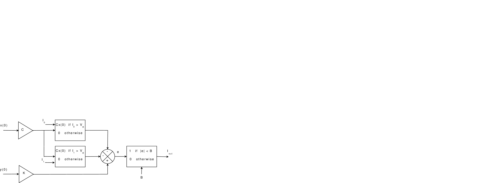
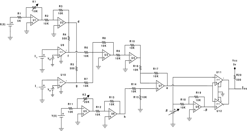
The block diagram of the electronic circuit of the dynamic logic gate is shown in Fig. 1. The simplicity of this circuit is due to the fact that the linear mathematical operation of commutation is performed by the comparators in the switching blocks, as is shown in Fig. 1. The first switching block checks if the input is a 0V or 5V and generates an output equal to 0V or , respectively. The second switching block does the same for the input . With the outputs of the two switching blocks and the input y(0) the input of the third switching block is estimated in order to produce the output of the logic gate. The schematic diagram of the dynamic logic gate circuit is shown in Fig. 2. It consists of eight operational amplifiers (from U1 to U8), four comparators (U9 - U12), 21 resistors (from R1 to R21), and two potentiometers and . Assuming ideal performance from all components, the circuit in Fig. 2 is modelled by the following set of equations in the nodes labelled as d, f, g and h. For the node d,
| (2) |
The voltages in the nodes f and g are given as follows
| (3) |
while the voltage at the node h is given by
| (4) |
Combining now the equations for the nodes d, f, g, and h one can get the voltage in the node e
| (5) |
Lastly, the outputs of comparators and as functions of the voltage in the node e are
| (6) |
Relating the equations (2) to (6) and taking the
values for the components given in Table 2 one can get
the output voltage of the circuit. As a
function of and , it is given
by the following set of equations:
| Components | Value |
|---|---|
| Resistors: | 1 |
| Resistors: | 10 |
| Resistors: | 500 |
| Potentiometer: | 10 |
| Potentiometer: | 20 |
| Op. Amplifiers: | TL081 |
| Comparators: | LM311 |
| (7) |
where and .
| (8) |
3. Experimental Results
The initial conditions and were taken equal to . The inputs and of the dynamic logic gate take only two values and in order to represent the binary values 0 and 1, respectively. The voltage is the transition voltage between (logic 0) and (logic 1). The different basic logic gates were obtained varying the value of the potentiometer at fixed value of the potentiometer , e.g., for a given value of the potentiometer , tuning the value of the potentiometer is required in order to get the desirable logic gate. The value of is adjusted by means of a variable source. We implemented this design on a printed circuit board (PCB) manufactured in our laboratory. In the experimental circuit, we used the TL081 operational amplifiers and the LM311 comparators supplied with a power source at and soldered directly to the PCB without a socket. The voltage Vdc was supplied by a variable dc supply source with an output range of 0 - .
We show now how to obtain the different kinds of basic logic gates. For example, if the potentiometer is equal to the resistor then , and fixing the voltages of to , we get and . Equations (5) and (6) can be rewritten as follows
| (9) |
| (10) |
| When K : | The circuit behaves |
|---|---|
| as the following gate: | |
| NOR | |
| NAND | |
| XOR | |
| OR | |
| AND |
The parameter is controlled by the potentiometer and the intervals according to the values of the parameters and are given in Table 3.
We analyze three different cases for the parameter corresponding to , and , but other cases can be investigated in the same way. These values fix the value of to , and , respectively.
For , we have the following response in the node
| (11) |
The output given by equation (10) and taking the input given by equation (12) yields the following table
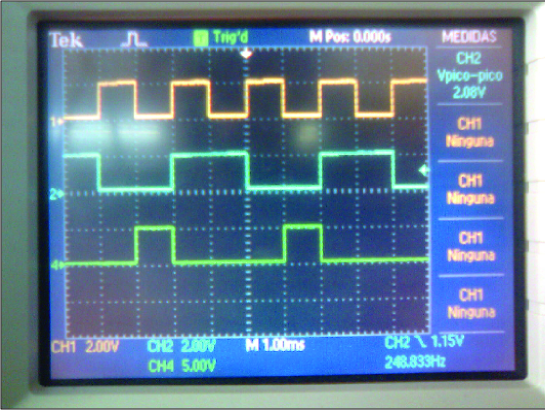
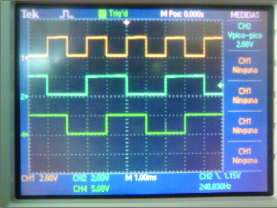
Considering that 0V is a logic zero and 5V is a logic one, then according to the inputs , and the output the dynamic logic gate behaves as a NOR gate as can be seen in Fig. 3.
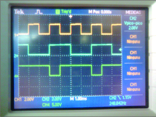
For this case, the experimental input-output signals of the NAND gate are shown in Fig. 4.
For , we have the dynamic logic gate behaving as a XOR gate. The input and output of the circuit are shown in the next equation and table
| (13) |
The experimental results are presented in Fig. 5.
The other logic gates can be checked in the same way for the
different values of the parameter .
4. Conclusions
A very simple dynamic logic gate electronic circuit has been described here together with its implementation using only analog components such as operational amplifiers, comparators and resistors. Its experimental behavior was tested and compared with the numerical behavior given by the mathematical model of the dynamical logic gate that has been taken from the work of Peng and collaborators [Peng et al., 2008]. Choosing different values of the potentiometer offers us the possibility to get different logic gates: NOR, NAND, XOR, and others. Such circuit realizations have many potential applications in chaos computing. Finally, we notice that our design can be manufactured in just one chip because the final electronic circuit contains only semiconductors and passive components.
References
Sinha, S., Ditto, W.L. [1998] “Dynamics based computation,” Phys. Rev. Lett. 81, 2156-2159.
Sinha, S., Ditto, W.L. [1999] “Computing with distributed chaos,” Phys. Rev. E 60, 363-377.
Kuo, D. [2005] “Chaos and its computing paradigm,” IEEE Potentials 24, 13-15.
Munakata, T., Sinha, S., Ditto, W.L. [2002] “Chaos computing: implementation of fundamental logical gates by chaotic elements,” IEEE Trans. Circuits Syst., I: Fundam. Theory Appl. 49, 1629-1633.
Murali, K., Sinha, S., Ditto, W.L., Bulsara, A.R. [2009] “Reliable logic circuit elements that exploit nonlinearity in the presence of a noise floor,” Phys. Rev. Lett. 102, 104101.
Murali, K., Miliotis, A., Ditto, W.L., Sinha, S. [2009] “Logic from nonlinear dynamical evolution,” Phys. Lett. A 373, 1346-1351.
Murali, K., Sinha, S., Mohamed, I.R. [2005] “Chaos computing: experimental realization of NOR gate using a simple chaotic circuit,” Phys. Lett. A 339, 39-44.
Murali, K., Sinha, S., Ditto, W.L. [2003] “Implementation of NOR gate by a chaotic Chua’s circuit,” Int. J. Bif. and Chaos 13, 2669-2672.
Peng, H., Yang, Y., Li, L., Luo, H. [2008] “Harnessing piecewise-linear systems to construct dynamic logic architecture,” Chaos 18, 033101.