Characterization of a broad energy germanium detector and application to neutrinoless double beta decay search in
Abstract
The performance of a 630 g commercial broad energy germanium
(BEGe) detector has been
systematically investigated. Energy resolution, linearity, stability vs.
high-voltage (HV) bias, thickness and uniformity of dead layers have been
measured and found to be excellent.
Special attention has been dedicated to the study of the detector response
as a function of bias HV. The nominal depletion voltage being 3000 V, the
detector under investigation shows a peculiar behavior for biases around 2000 V: in a
narrow range of about 100 V the charge collection is strongly
reduced. The detector seems to be composed by two parts: a small volume
around the HV contact where charges
are efficiently collected as at higher voltage, and a large volume where
charges are poorly collected. A
qualitative explanation of this behavior is presented. An event-by-event pulse
shape analysis based on / (maximum amplitude of the current pulse
over the total energy released in the detector) has been applied to events in different
energy regions and found very effective in rejecting non localized events.
In conclusion, BEGe detectors are excellent candidates for the
second phase of GERDA, an experiment devoted to neutrinoless double
beta decay of 76Ge.
keywords:
Gamma detectors, Particle identification methods1 Introduction
This paper deals with the characterization of a 630 g broad energy germanium
(BEGe) detector [1], a commercial high-purity Ge detector with a small
read-out electrode which is manufactured by Canberra
Semiconductor [2]. The work is part of
the general effort of the GERDA collaboration to improve the understanding of
these detectors which will be employed in the second phase of the experiment.
Preliminary results obtained with the detector under investigation
have been already presented in Refs. [3, 4].
A detector with the same contact geometry, differing only for dimensions, has
been previously investigated in the framework of the GERDA
activities [5, 6, 7].
The GERDA (GERmanium Detector Array)
experiment [8], which recently started its commissioning phase at the
underground Gran Sasso Laboratory of the INFN (Italy), is devoted to the study of
the neutrinoless double beta decay of 76Ge with a
large mass of detectors isotopically
enriched in 76Ge; about 40 kg are planned for the final configuration.
In searching for rare processes, like neutrinoless
double beta decay, two parameters
are extremely important: energy resolution and background. Substantial background
reduction can be achieved by a careful selection of materials used in the
set-up construction (not considered in this paper) and by an efficient data
analysis which needs in turn a deep knowledge of the detector
characteristics.
The characterization of the BEGe detector was divided into two parts:
experimental investigation of the detector features; modeling of the detector
signal formation and development.
The present note describes the experimental part while the detector modeling is
presented and discussed in Ref. [9] (companion paper).
The paper is organized as follows: Sect. 2 summarizes the
detector specifications provided by the manufacturer and the performance in
terms of active volume, linearity and energy resolution. In
Sect. 3 the detector response to radiation sources
at different bias high voltages is described and discussed. A peculiar behavior
of some BEGe detectors, already reported in Refs. [3, 10, 11],
is reproduced experimentally and discussed in details.
Sect. 4 reports the performance of the detector in
the discrimination of single-site to multi-site events by the analysis of
the shape of the pulse signal. Finally, outlook and conclusions are presented in
Sect. 5.
2 Detector specifications and performance
The detector under study is a commercial p-type broad energy germanium (BEGe) detector (model BE3830/s) manufactured by Canberra Semiconductor. The detector has a cylindrical shape with a diameter of 71 mm and a thickness of 32 mm. There is a small Boron-implanted electrode on one of the flat surfaces. The Lithium-diffused electrode covers the rest of the outer surface and it is separated from the electrode by a circular groove. The detector is mounted in a 1.5 mm thick cylindrical aluminum housing. A schematic view of the BEGe detector and of its housing is presented in Fig. 1.
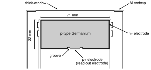
The positive bias voltage is applied to the electrode while the electrode (signal read-out electrode) is grounded. The detector specifications and performance according to the manufacturer data sheet are summarized in Tab. 1. The bias voltage recommended by the manufacturer and used in most the measurements is 3500 V.
| Physical characteristics: | |
|---|---|
| Active diameter | 71 mm |
| Active area | 3800 mm2 |
| Thickness (active) | 32 mm |
| Distance from entrance window | 5 mm |
| Window thickness (Al) | 1.5 mm |
| Dead layer thickness | 0.8 mm |
| Electrical characteristics: | |
| Depletion voltage | Vdc |
| Recommended bias voltage | Vdc |
| Energy resolution at 1.332 MeV: | |
| FWHM | 1.752 keV (4 s shaping time) |
| FW(1/10)M | 3.259 keV (4 s shaping time) |
2.1 Data acquisition systems
The charge signal coming from the small read-out electrode is sent to the charge-sensitive pre-amplifier model 2002CS integrated in the detector housing. The pre-amplifier output signals are processed using two different Data Acquisition (DAQ) systems, according to the aims of the measurement considered:
-
1.
A standard analogue electronic chain, with a spectroscopy amplifier Ortec 672 and a multichannel Ethernim ADC. The data are then analyzed using the software MAESTRO-32 or GammaVision-32 provided by Ortec [12].
-
2.
A digital chain, in which the pre-amplifier output signals are fed to a CAEN 4-channel digitizer (module N1728B), with sampling frequency of 100 MHz and 14-bit resolution [13]. The digitizer is controlled by a computer connected via USB and running the TNT-TUC program distributed by CAEN [14]. The digitized signals are transferred to the computer and analyzed by a set of ad hoc programs [15]. Traces are acquired for 40 s, including a 10 s baseline before the signal.
2.2 Linearity
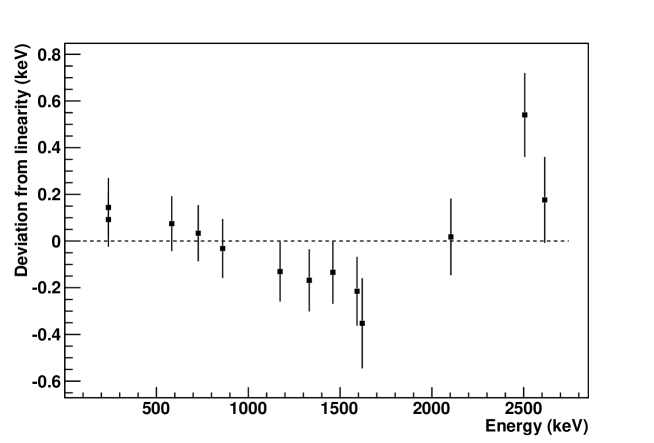
First, the linearity of the analogue electronic chain has been tested with an Ortec Research Pulser module 448. It results to be better than 0.01%. Then the global linearity of the system (i.e. detector and analogue electronic chain) has been verified irradiating the crystal with 60Co and 228Th sources. Deviations from linearity were found to be less than 0.02% in the energy range from 239 keV up to 2.614 MeV. Fig. 2 shows the residuals of a linear fit, i.e. the differences between data and the values expected from the fit.
The linearity obtained with the digital DAQ system and the off-line energy reconstruction is slightly worse, but in any case better than 0.05%.
2.3 Energy resolution
The energy resolution of the detector was studied by irradiating the crystal
with a 228Th and a 60Co source.
The resolution obtained with the analogue DAQ system at the 60Co lines
is compiled in Tab. 2 for different shaping times.
The energy resolution achieved for 6 s shaping time at the 1332 keV
60Co line is keV FWHM, which is better than the manufacturer
specification.
Fig. 3 shows the
energy resolution as a function of the energy for the 228Th and 60Co
peaks in the spectra recorded by the analogue DAQ system.
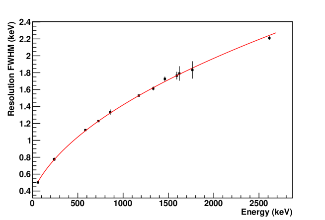
The behavior is well described by the parametrization
| (1) |
with and ; the fit has with 11 d.o.f.
| Shaping time | 1173 keV | 1332 keV | |
|---|---|---|---|
| 3 s | FWHM | 1.74 | 1.82 |
| FW(1/5)M | 2.62 | 2.84 | |
| FW(1/10)M | 3.23 | 3.53 | |
| 6 s | FWHM | 1.53 | 1.56 |
| FW(1/5)M | 2.26 | 2.44 | |
| FW(1/10)M | 2.56 | 2.81 | |
| 10 s | FWHM | 1.51 | 1.59 |
| FW(1/5)M | 2.31 | 2.41 | |
| FW(1/10)M | 2.74 | 2.90 |
Similar results were obtained also with the digital DAQ system.
2.4 Volume scanning and dead layer thickness
The study of the active volume and of the dead layer features was divided into
two parts. Firstly, the detector active volume and the uniformity of the dead layer
were investigated by scanning the detector surface with a collimated
241Am source. Secondly, the average thickness of the dead layer was estimated
by irradiating the detector with an uncollimated 133Ba source.
To perform the first set of measurements a mechanical device was built to allow
the positioning of collimated sources with sufficient accuracy along the diameter
of the front face and the side of the detector. The collimator had a hole
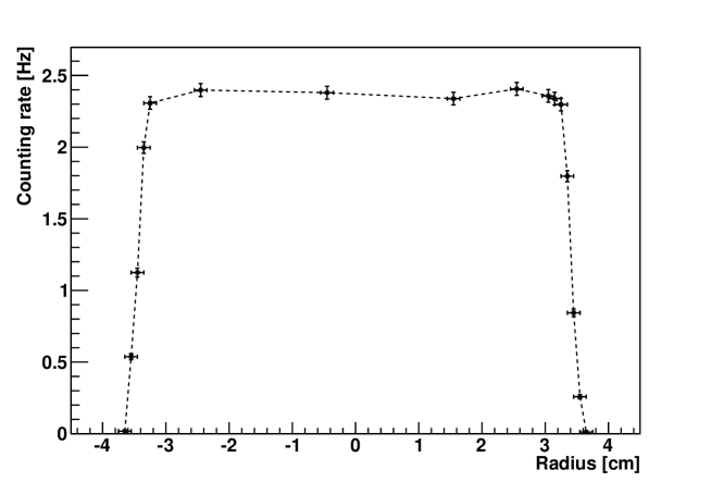
of 1 mm diameter and a length of 34 mm. Using a collimated beam of low-energy
photons (59.5 keV) from the 241Am source allows to obtain
well-localized interactions close to the surface. Consequently, the dead layer
thickness is related to the counting rate in the 59.5 keV line.
Fig. 4 shows the counting rate vs. the radial position
on the top surface of the detector. The diameter of the active volume, defined
as the width with count rate above 50%(90%) of the central plateau,
is 68.6(65.9) mm.
The flatness of the central plateau indicates also that the
thickness of the top dead layer is fairly uniform.
The vertical scanning of the detector yielded less accurate results
because of the presence of the lateral copper holder and of its reinforcing rings
(see Fig. 1).
The estimated vertical dimension of the active volume is about 30 mm.
The detector has been also scanned moving the source along
a circle centered on the detector symmetry axis, on the top surface
of the end-cap. Data were used for the validation of the BEGe detector
modeling and of the pulse shape simulation [9].
The average thickness of the dead layer has been measured by studying the ratio
of the intensities of the 133Ba -lines at 81 keV and 356 keV. An
uncollimated 125 kBq 133Ba source has been used for this purpose.
The ratio between the two intensities vs. the thickness of the dead layer has
been predicted by means of a Monte Carlo simulation based on the GERDA software
framework MaGe [16]. The dead layer thickness on the top of the detector
which is necessary to reproduce the experimental ratio , as
displayed in Fig. 5, is:
| (2) |
in good agreement with the manufacturer specifications. The systematic uncertainties are due to the Monte Carlo modeling of the detector and to the parametrization of the vs. thickness curve, as shown in Fig. 5.
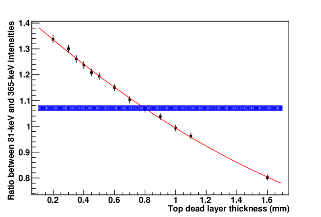
The average dead layer thickness on the side of the detector is mm (statistical and systematic uncertainties combined in quadrature).
3 Detector response at different bias high voltages
The BEGe detector response as a function of the bias high
voltage (HV) was studied by irradiating the Ge crystal with an uncollimated
137Cs source, which emits a single -ray line at 662.3 keV.
The source was placed on the front face of the detector, on its vertical
symmetry axis, a few mm above the end cap.
Since the source is uncollimated and the total attenuation length of
662-keV -rays in metallic germanium is about 27 mm, the detector
volume illumination is approximately uniform.
Charge pulses have been collected with the digital DAQ system
described in Sect. 2.1. For this particular dataset,
pulses have been sampled for 100 s
(trigger after 50 s, for a solid baseline estimation) at
100 MHz rate.
Energy is hence reconstructed from the charge pulses
according to the Jordanov algorithm [17], using an integration time of
12 s.
The amplitude for the 137Cs full-energy peak (FEP) and the counting rate
were measured different for bias high voltages. Starting from the nominal operation
voltage of 3500 V the HV was decreased. The total count rate and the rate in the
FEP remain
fairly constant down to 2300 V, as shown in Fig. 6. This
suggests that the actual depletion voltage of the detector is about 2300 V,
a value much lower than the manufacturer specification.
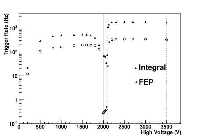
When the HV is decreased below 2300 V, only a modest and smooth degradation is
observed, as expected for HV values below the depletion voltage.
But the further reduction of the HV below 2100 V causes a sudden change in the detector operation.
In a voltage interval of about 100 V the integral counting rate is reduced by a factor of 20
with respect to what is observed above 2200 V. Similarly, the counting rate at
the FEP is suppressed by three orders of magnitude with
respect to the rate at 2200 V.
Below this anomalous voltage interval, the counting rate returns close to the value
before the dip and resumes the previous smoothly decreasing trend.
Such a peculiar behavior has been reported in previous works [3, 10] but
- at our knowledge - never discussed nor experimentally investigated in detail.
In addition, it has been verified that other BEGe detectors supplied by the same
manufacturer differing only for the dimensions do not show such a peculiar behavior
in their HV curves [18].
Fig. 7 shows the energy spectra (normalized for the live
counting time) generated by the 137Cs source at three different bias
voltages: 3500 V (nominal), 2090 V and 2010 V. In all cases, pulse amplitude
is converted to energy using the calibration data acquired at 3500 V. Energy
calibration at 2010 and 2090 V should be hence regarded as indicative only.
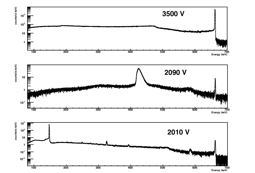
It can be seen that
for HV values in the anomalous interval, the FEP at 662 keV is strongly suppressed
in rate, while its position is practically unaffected.
The suppression factor is 700 at 2090 V and 1100 at 2010 V.
In addition, new spurious peaks appear at lower energies, with much higher
counting rate than the FEP.
At 2090 V there is a broad peak at 426 keV equivalent energy, whose FWHM is about 12 keV,
while at 2010 V (and in general, in the range 2000-2070 V) a narrow peak appears at
keV equivalent energy111Notice, that other small spurious peaks visible at 2010 V
are due to lines at higher energy from environmental radioactivity. For
instance, the line at about 325 keV equivalent energy is related to
the 1460 keV -ray from 40K, which is present in the background spectrum..
To investigate the origin of these new structures, we studied the shapes of the signals populating the different peaks. Fig. 8 shows the average signals accumulated for the spurious and for the full energy peaks. The averaging of the signals provides a pulse shape which is statistically representative of the peak population and allows to reduce the noise.
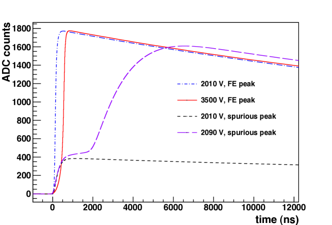
The average pulse accumulated for the FEP at 3500 V is an example of a common pulse
expected from BEGe detectors. The signal has a slow rising part at the beginning
followed by a leading edge at the end [9]. The average 10%-90%
rise time of the normal pulses is about 300 ns.
The pulses populating the 426 keV spurious peak at 2090 V are characterized by
two rising parts connected by a plateau between 0.4 and 2 s.
While the first rising part (0–400 ns) is fast, the second one (2–4 s)
is extremely slow.
For such a long collection time, part of the charge is expected to be lost by
trapping.
However, the pulse has a total amplitude comparable with
the signals of the normal events populating the FEP at 3500 V.
Besides the charge loss by trapping, the underestimation of the peak energy and its
asymmetric shape is due to
ballistic deficit since the shaping parameters are tuned for faster pulses.
The broadening may be due either to the analysis algorithm
or - more likely - to high-voltage instabilities. In this regime small
fluctuations of the bias voltage have a significant impact on the peak
position.
Differently, the spurious peak at 2010 V originates from
fast signals (rise time of about 400 ns) which have an amplitude
clearly smaller (by a factor of five) than the signals creating the FEP.
The shape of the pulses of the FEP at 2010 V is similar to that observed
at 3500 V, even if the average rise time is significantly faster
(rise time is about 200 ns).
This peculiar behavior was investigated by using the simulation described in
Ref. [9] and was connected to the electric field
configuration inside the detector.
As shown in Ref. [9], the electric field of BEGe detectors
operated at the nominal bias voltage (e.g. 3500 V) reaches
its minimum strength in the middle of the detector.
The holes generated by interactions close to the electrode are collected in
the center of the detector and then drift along the same trajectory to the small
read-out electrode (“type I” trajectories in Ref. [9]). Therefore, the
last part of the signals is independent of the interaction position for most of the
detector volume ( of the total active volume).
The interactions occurring close to the small electrode originate a second
class of pulses (“type II-III” trajectories in Ref. [9]). These
signals have a faster rise time because the holes generated are not collected in
the center of the detector but directly at the read-out electrode.
Decreasing the HV (starting from the operational bias voltage) results in a
reduction of the electric field strength inside the detector.
When the electric field approaches zero the recombination
probability of the holes increases [19] leading to a change in the charge
distribution inside the Ge crystal which contributes to the total electric
field.
The starting of this recombination process ( V for our detector)
defines the depletion voltage of the detector.
Even if our simulation tools can not provide an accurate computation of the
electric field in the anomalous voltage interval, we estimate that
the electric field in the middle of the detector is extremely weak for HV values
between 2100 V and 2300 V (“configuration A”).
Moreover, we qualitatively expect that around 2000 V the electric potential has two minima
placed in the small electrode surface and in the center of the detector, respectively.
In this configuration both the small electrode and the center of the detector act as collection
sites for the holes (“configuration B”).
Below 2000 V the two collection sites merge creating a conducting non-depleted
region which expands when the HV is further decreased.
This region approaches the junction when the bias voltage is removed.
This model can explain the features of the average pulses in Fig. 8.
In the “configuration A” the holes generated by “type I” events are
collected in the center of the detector and then drifted to the read-out
electrode.
The plateau of the pulses in the spurious peak at 2090 V corresponds to the slowing
down of the hole drift in the middle of the detector where the electric
field is weak.
In the “configuration B”, part of the holes are collected and trapped
in the middle of the detector and do not reach the read-out electrode.
The corresponding signals have a smaller amplitude, defined by the
value of the weighting potential in the middle of the detector [9].
The reduction of the signal amplitude observed in Fig. 8
is in good agreement with the simulation results.
Moreover, the amplitude of this signal corresponds to the amplitude at the plateau
of the pulses in the spurious peak at 2090 V.
In fact, the second collection site in the middle of the detector should
originate in the region of low electric field at 2090 V.
According to our model, only the “type I” trajectories which pass through the
center of the detector should populate the spurious peaks.
The pulse shape for events
close to the read-out electrode (“type II-III”) is only slightly affected by
differences in the electric field due to different bias voltages; therefore,
these events eventually populate the FEP.
This is consistent with the fact that the FEP is always present - at the same
position - also for HV values in the anomalous interval, although its rate is
suppressed, as displayed in Fig. 7. Furthermore, the rise time
of the FEP pulses at 2010 V is shorter than that at 3500 V because only
the “type II-III” signals are present.
To estimate the volume of the detector originating the spurious peaks we
performed a set of measurements with a collimated 137Cs source, scanning
the top surface and the side of the detector.
The spurious peaks are strongly suppressed when only the region
close to the small read-out electrode is irradiated. They are instead enhanced
when the top surface of the detector is illuminated.
We qualitatively estimated that the volume originating the FEP at the
anomalous HV values has a radius and a height of the order of 1 cm.
The region is a few percent of the total active volume and corresponds to the
region which is expected to originate “type II-III” pulses [9].
The peculiar behavior of the considered BEGe detector (dip in the
HV response, pulse shapes) is due to a specific combination of geometrical
and intrinsic characteristics (e.g. the impurity concentration) and it is not
observed in some other BEGe detectors provided by the same manufacturer.
For instance, the dip in the HV curve is not observed in two BEGe detectors
produced by Canberra with Ge isotopically depleted in 76Ge [20] and
characterized within the GERDA activities [18]; the detectors are modified versions of
Canberra BE5030/S, having 74.5 mm active diameter and 33 mm height.
4 Pulse shape analysis
The excellent performance of BEGe detectors in discriminating single-site
events (SSE) from multi-site events (MSE) was recently reported [5, 6].
A SSE is characterized by a single energy deposition localized in a
volume. On the other hand, MSE consist of several
interaction sites separated by a typical distance of the order of 1 cm
(e.g. Compton scattering).
Such a feature is of primary interest for experiments like GERDA looking for neutrinoless
double beta decay (DBD). Indeed, genuine DBD events are generated by two
electrons that have a range of less than 1 mm in germanium and hence belong
to the former category of events. The background due to
-rays is typically multi-site, because -rays in the energy range
of interest mainly undergo Compton scattering with mean free path
of a few centimeters in germanium.
Therefore, an efficient MSE vs. SSE discrimination allows to reject
-induced background, while preserving genuine DBD events.
In Ref. [5, 6] a discrimination method based on the ratio
between the maximal current (maximal amplitude of the current pulse)
and the total energy released in the crystal was proposed and validated.
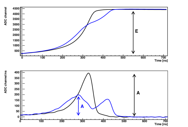
As shown in Fig. 9, the events can be classified as single-site if the
value of the parameter is higher than a given threshold . More details
about this subject are provided in Ref. [9].
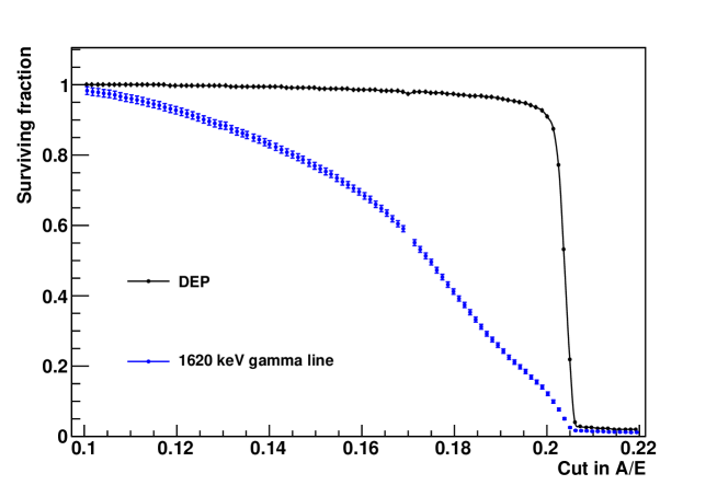
The rejection power of our detector has been tested irradiating the Ge crystal with a 228Th source. The maximum of the current pulse has been calculated numerically from the digitized charge pulses, after having applied a 50-ns average filter to reduce the noise. The fraction of surviving events as a function of the value of the threshold has been determined for the double escape peak (DEP) of the 2614-keV -line of 208Tl and for the full-energy -ray peak at energy 1620.5 keV from the 212Bi decay. In fact, the sample in the DEP is highly enriched in single-site events, since it is originated by the full absorption of the kinetic energy of the e+-e- pair created by the -ray when both annihilation quanta escape. Therefore, the peak energy is EDEP=keV. Being impossible to distinguish double escape from Compton scattering events in the same energy range on an event-by-event basis, the populations are separated statistically, by fitting the energy spectrum with a Gaussian peak plus a linear background. Similarly, the 212Bi peak is dominated by multi-site events and is used to estimate the rejection efficiency of -ray events. In the following survival probabilities are quoted with respect to the peaks only, namely having subtracted the Compton continuum. As shown in Fig. 10, can be tuned to achieve an acceptance as high as 90% for the DEP, while keeping only 10% of the 212Bi peak.
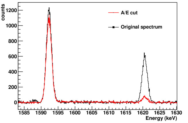
The comparison of the DEP line and the 212Bi line before and after the / cut when the DEP acceptance is fixed at 90% is shown in Fig 11.
Keeping the DEP acceptance fixed at 90% the discrimination power has been evaluated also in other energy regions of interest, i.e. the 208Tl full energy peak (FEP) at 2614 keV, the single escape peak (SEP) of 208Tl (ESEP=2103 keV) and the Compton continuum in a 20-keV region around the value of 76Ge (2039 keV).
| FEP | SEP | FEP | Qββ |
| 2614 keV | 2103 keV | 1620 keV | 203910 keV |
| 6.40.1 | 6.20.4 | 11.50.1 | 37.50.5 |
The results are summarized in Tab. 3:
the intensity of full-energy -ray lines can be
suppressed by a factor of 10, while the Compton continuum can be reduced by a
factor of 3 in the region of interest around the value of
76Ge.
The continuum at is in general a mixture of SSE and MSE,
produced by single- and multiple-Compton scattering of
higher energy -rays, respectively. The
survival probability after the cut
for events in the continuum at
is hence related to the fraction of genuine
single-site Compton events. On the other hand, the ratio of the SSE and MSE
populations in the Compton continuum depends on the specific configuration
of the 228Th source and of the experimental set-up, including the external
shielding. The acceptance of the cut for genuine single-site events at
could not be assessed experimentally, but it can be estimated
by Monte Carlo simulations, as reported in Ref. [9].
5 Conclusions
The performance of a 630 g commercial BEGe detector (model B3830/S by Canberra) has been systematically investigated and found to be excellent. A peculiar behavior has been observed in its response as a function of the bias high voltage: for biases around 2000 V (to be compared to the nominal depletion voltage, 3000 V) there is a narrow range of about 100 V where charge collection is strongly reduced. This is related to the electric field configuration inside the crystal, since in that range of bias voltages a very weak field is expected to be present in the central part of the detector, that extends up to collecting electrode and prevents the full charge collection. An interesting feature of BEGe detectors, mainly for experiments looking for neutrinoless double beta decay, is their pulse shape discrimination capability of single-site vs. multi-site events based on the parameter. It is possible to reject more than 90% of -ray events while having 90% of surviving events for genuine SSE. These results are in agreement within a few percent with the ones obtained in Ref. [5] with a detector of the same type, but with a larger diameter (80 mm). Note also that spectroscopic performance is remarkably stable in a wide range of bias high voltage above 2400 V.
Acknowledgements.
We would like to thank our GERDA Collaborators for very useful discussions, as well as the staff of the Gran Sasso laboratory for the precious help and support.References
- [1] CANBERRA Broad Energy Ge (BEGe) Detector, catalog accessed at URL: \hrefhttp://www.canberra.com/products/485.asphttp://www.canberra.com/products/485.asp
- [2] Canberra Semiconductor NV, Lammerdries 25, B–2430 Olen, Belgium.
- [3] A. di Vacri et al., Characterization of Broad Energy Germanium Detector (BEGe) as a candidate for the GERDA experiment, IEEE Nucl. Sci. Symp., Conf. Record 2009 (2009), 1761.
- [4] M. Agostini, Characterization of a Broad Energy Germanium detector through advanced pulse shape analysis techniques for the GERDA double-beta decay experiment, Master Thesis, Università di Padova (2009).
- [5] D. Budjáš, M. Barnabé Heider, O. Chkvorets, N. Khanbekov and S. Schönert, Pulse shape discrimination studies with a Broad-Energy Germanium detector for signal identification and background suppression in the GERDA double beta decay experiment, JINST 4 (2009), P10007.
- [6] D. Budjáš, M. Heisel, W. Maneschg and H. Simgen, Optimisation of the MC-model of a p-type Ge-spectrometer for the purpose of efficiency determination, Appl. Radiat. Isot. 67 (2009) 706.
- [7] M. Barnabé Heider, D. Budjáš, K. Gusev and S. Schönert, Operation and performance of a bare broad-energy germanium detector in liquid argon, JINST 5 (2010), P10007.
- [8] GERDA Collaboration, I. Abt et al., GERDA: The GERmanium Detector Array for the search of neutrinoless decay of 76Ge at LNGS, Proposal, \hrefhttp://www.mpi-hd.mpg.de/ge76http://www.mpi-hd.mpg.de/ge76.
- [9] M. Agostini et al., Signal modeling of HP-Ge detectors with a small read-out electrode and application to neutrinoless double beta decay search in 76Ge, companion paper, submitted to JINST, preprint [arxiv:1012.4300].
- [10] D. Budjáš, Germanium detector studies in the framework of the GERDA experiment, Ph. D. thesis, University of Heidelberg (2009).
- [11] R. Cooper and D. Radford, talk given at “Workshop on Germanium-Based Detectors and Technologies”, Berkeley, May 18-20, 2010.
- [12] ORTEC Advanced Measurement Technology, Inc., catalog at \hrefhttp://www.ortec-online.com/Solutions/gamma-spectroscopy.aspxhttp://www.ortec-online.com/Solutions/gamma-spectroscopy.aspx
- [13] See URL \hrefhttp://www.caen.it/nuclear/product.php?mod=N1728Bhttp://www.caen.it/nuclear/product.php?mod=N1728B.
- [14] See URL \hrefhttp://www.iphc.cnrs.fr/-TUC-.htmlhttp://www.iphc.cnrs.fr/-TUC-.html.
- [15] M. Agostini, L. Pandola, P. Zavarise and O. Volynets, GELATIO: a general framework for modular digital analysis of HPGe signals, in preparation.
-
[16]
M. Bauer et al., MaGe: a Monte Carlo framework for the Gerda and Majorana double
decay experiments, J. Phys. Conf. Ser. 39 (2006) 1;
M. Boswell et al., MaGe: a Geant4-based Monte Carlo application framework for low background germanium experiments, submitted to IEEE, Trans. Nucl. Scie., preprint [arxiv:1011.3827.v1]. - [17] V.T. Jordanov and G.F. Knoll, Digital synthesis of pulse shapes in real time for high resolution radiation spectroscopy, Nucl. Instrum. and Meth. A 345 (1994) 337.
- [18] G. Pivato, Experimental characterization of a Broad Energy Ge detector for the GERDA experiment, Master Thesis, Università di Padova (2010).
-
[19]
S.M. Sze, Physics of Semiconductor Devices, John Wiley & Sons, 1981.
S. Selberherr, Analysis and Simulation of Semiconductor Devices, Springer-Verlag, 1984. - [20] M. Agostini et al., Procurement, production and testing of BEGe detectors in 76Ge, to appear in Nucl. Phys. B, Proc. Suppl. (Neutrino 2010).