Modified graphene with small BN domain: an effective method for band gap opening
Abstract
BN domains are easy to form in the basal plane of graphene due to phase separation. With first-principles DFT calculations, it is demonstrated theoretically that the band gap of graphene can be opened effectively around K (or K’) points by doping the small BN domains. It is also found that the random doping with B or N is possible to open a small gap in the Dirac points, except for the modulation of Fermi level. The surface charge which belongs to the states near Dirac points is found to be redistributed locally. The charge redistribution is contributed to the change of localized potential due to the doping effects. This may be the reason that the energy states near Dirac points is just disturbed in the energy region [-0.4eV, 0.4eV] for the doping of BN domain. Thus, we suggest that the band opening induced by the doped BN domain is due to the breaking of localized symmetry of the potential. Doping graphene with BN domains is an effective method to open a band gap with quasi-linear dissipation near Dirac point.
- PACS numbers
-
71.20.-b, 81.05.Uw, 71.10.-w
I Introduction
Graphene, consisted of a stable monolayer of carbon atoms with honeycomb lattice, has attracted enormous attentionc1 ; c2 ; c3 ; c4 recently due to the fascinating physical propertiesc5 , such as abnormal quantum Hall effectsc6 and massless Dirac fermionsc7 , which is attributed to the special linear behavior of electronic band near Fermi level in (or ) points of Brillouin zone. However, the linear gapless spectrum of graphene conflicts with the basic requirement for its application in traditional electronic devicesc8 ; c9 , since in the most microelectronic devices, such as field-effect transistors, the active material for the transport layer needs the presence of energy gap by which the conducting behavior of electrons or holes as charge carrier can be controlled with the voltage. Therefore, with the expectation of bandgap in graphene energy spectrum, the design of its band structure has spurred an intense scientific interest. Many different methods have been test to modulate the electronic properties of graphenec10 ; c11 ; c12 ; c13 ; c14 ; c15 ; c16 ; c17 .
For engineering the band gap, these mechanisms tested can be divided into three aspects. Firstly, with quantum limit effect of size, the gap is possible to be opened by tweaking the width or carving graphene into some geometryc12 ; c18 , such as graphene nanoribbon. Secondly, it is to interact with different substratesc19 , such as BN layer or [0001] SiC substratec11 , or to use electronic field with two-layer graphene to break the symmetry of graphene for gap openingc10 ; c14 ; c16 . Thirdly, modulating the electronic properties is by functionalizing the graphenec15 ; c17 ; c20 ; c21 . For examples, introducing Stone-Wales defectsc13 in the graphene layer, physically absorbing some chemical molecules on graphenec20 and hydrogenation of graphenec17 . Despite these recent progresses, an effective method for band gap opening still remains to explore. It is noticed that the difficulty of controlling the edge with scissor technique, the complex of electrically gated bilayer graphene, the weak disturbance to the electrons of graphene layer with physical absorption and the destroy of planar network of graphene with chemical absorbtion. It is also possible to be an effective method that using traditional alloying mechanism to modulate the band gap at () points of graphene. Unfortunately carbon stays the second row of the table and it is difficult to find an appropriate element to alloy the carbon with 2D structures. Considering the compound BN is from the two elements near the carbon, we will explore systematically the change of electronic properties of graphene by alloying graphene with small concentration of Boron nitride (BN).
BN is isoelectronic to carbon with similar structures, for examples 3D structures cubic-BN and diamond, 2D layer structures hexagonal-BN and graphite. It is known that BN sheet is with large band gap. Thus, it is possible that the band gap will be opened effectively by alloying graphene with BN. However, we have the experience that BN is difficult to be solubilized with carbon for any structures, such as, cubic phase, sheet structure and fullerene-like structures. This is mostly contributed that the B-N and C-C bonds with large bonding energy is stronger than the B-C and N-C bonds and result in the phase separation with carbon region and BN region. However, by properly controlling the growth process, the BCN nanostructures with the rich variety of physical properties can be synthesizedc22 ; c22b , such as the report about single layer graphene with BN large domains by hybridizing BN and graphenec22 . By the controlling of the thermodynamic process or chemically introducing the hybridization of graphene and BN molecule or molecule, the graphene with small BN domains will be possible to be gained, since the lattice constants of graphene is just a little difference from that of BN sheet which makes the strain energy is small in the process of alloying and the graphene fragment will be connected with small BN domain in the thermodynamic process. In this paper, we will show theoretically that the band gap of graphene can be opened effectively around (or ) points with alloying the small BN domains under the limit of low concentration, even under that of the concentration for doping with BN domains.
With the density functional calculations, we explore firstly the doping effect of B and N in graphene. With the unexpected case, the doping effect on the 2D sheet graphene is different from that on the 3D case of usual semiconductors. As expected, the B atom is less an electron than C atom and the doping of B will result in the down-shift of Fermi level for obtaining the hole as carrier. The N atom is more an electron than C atoms and the doing of N will induce the up-shift of Fermi level for gaining the electron as carrier. Surprisingly, the B or N doping can open a gap around Dirac point in the special case. Then we studied the question carefully by analyzing the calculation. For the doping or alloying of small BN domain, we detect the change of band structures and the effect of band opening for the incorporation of BN molecule, (BN)3 and (BN)12 for each concentration. With the analysis of charge redistribution and potential redistribution due to the introduction of small BN domain, it is found that the surface charge states of graphene which belongs to the electrons is sensitive to the redistribution. Thus, we suggest that the redistribution of surface charge which breaks the local symmetry of graphene is the main reason of band gap opening of graphene. In additional, the coulomb dipole from BN molecule may be also important to the breaking of symmetry of graphene structure and thus to the band gap opening.
II Choice of Structures and Computational method
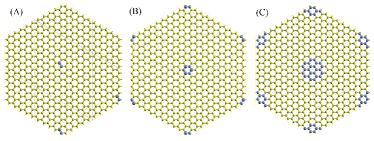
To model the 2D graphene with alloying or doping the B, N and different BN domains, the supercell approach is used for the structures. In order to avoid the spurious coupling effect along -axis due to the periodic images, the vacuum separation in the model structures is set to 15 Å. The graphene plane models are constructed from hexagonal and unit cells, respectively. For alloying or doping the small BN domains, we consider the BN molecule, (BN)3 and (BN)12 to merge into the graphene basal plane, as shown in Fig.1.
In the present work, the accurate frozen-core full-potential projector augmented-wave (PAW) method, as implemented in the Vienna initio simulation package (VASP)c23 ; c24 is used. With density functional theory, the electronic density with the exchange and correlation effects is computed under the local density approximation (LDA). The k-space integral and plane-wave basis, as detailed below, are tested to ensure the total energy is converged at the 1 meV/atom level. The kinetic energy cutoff of 550 eV for the plane wave expansion is found to be sufficient and the Monkhorst-Pack method is used to choose k points in moment space. By the optimization process, the lattice constants of graphene and BN sheets obtained are 2.44Å and 2.48Å, respectively. The values are near the experimental value obtained at low temperature (2.46Å for graphene and 2.50Å for h-BN) with small underestimation. It is noticed that the electronic bands near surface is not very sensitive to the small change of lattice constant for the graphene and single layer BN sheet. Therefore, for the optimization of the systems with doping or alloying with low concentration, the lattice parameters are fixed with the consideration of Vegard’s law and the internal coordinates of atoms are relaxed fully. After relaxation of structures, the strain on the systems is very small and the relaxed structures are found to follow Vegard’s rules well.
III Results and Discussion
III.1 Doping pristine graphene by B and N
Due to the weaker bond energy of B-B and N-N than C-N and C-B, the boron or nitrogen is relatively easy to alloy with - hybridized carbon materials, such as graphite, CNT, graphene oxide and graphene. With the relaxation and optimization of the structure, it is found that the lattice constant just has a little change and the local strain is also small due to the introduction of B or N in the lattice of graphene as a doping effect. This means that the 2D planar structure is not destroyed due to the small amount of B, N and BN which is not like the effect of chemical absorption, such as hydrogen absorbed on graphene.
For the usual semiconductors, the point defect as an acceptor or donor is introduced into the lattice of host will induce an accepter energy level near the top of valance band or donor energy level near the bottom of conduction band in the band gap of the host’s energy spectrum and thus the formation of the -type or -type material. However, Duo to the zero band gap of graphene, it is possible that boron or nitrogen in the lattice matrix of graphene will result in the special defect energy level in valance bands or conduction bands which are contributed to the orbitals. As shown in Fig.2 C and D, the doping of B results in the down-shift of Fermi level and the doping of N results in the up-shift of Fermi level. With the thermal anneal of graphene ribbon in ammonia, the experiment have confirmed that the introduction of nitrogen can result in -doped graphene materialc25 .
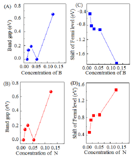
Near Dirac points, the linear dispersion can be expressed as , where is the momentum related to the Dirac points and is Fermi velocityc2 . With the linear relation, the density of states per unit cell can be given by , where is the unit cell area with the lattice constant =2.42Å. Thus, with the doping of small amount of dopant, the shift of Fermi level is related with the concentration of dopant by the relation (1), where is the concentration of boron or nitrogen. In the low concentration, the doping effect follows the tendency of formula (1), as shown in Fig. 2 C and D.
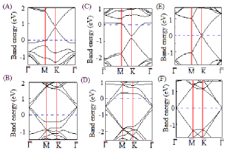
Though the boron or nitrogen in the lattice matrix of graphene does not induce any defect energy states near Dirac points, the band states near the Dirac points have been disturbed to some extent. As shown in Fig. 2 A and B, in some concentration, an energy gap is induced around the Dirac point. It may be considered that the symmetry of the two sublattices is broken by the doped boron or nitrogen is the important reason. However, this can not explain that the band gap is not opened in the B or N-doped graphene with () unit cell. We need to check the change of band structure of graphene due to the introduction of B or N. In Fig. 3, we compare the band structure of B- or N-doped graphenes to the prime graphenes with and unit cells. It is assured that there are not the localized defect states in the energy spectrum of doped graphene. This may be attributed to the strong interaction of B (or N) and C and the small difference of electronegativity, with the -hybridization. For B-doped graphene, a new hybridized band around -1.0 -1.5 eV under Dirac point is formed. For N-doped graphene, there is a new hybridized band at about 1.0 eV above the Dirac point. The new band affects strongly the band structure near energy ranges and thus the charge will be possible to be redistributed (see the subsection below for details). Therefore, the bands near the Dirac points will be disturbed. For the lattice with unit cell, the Dirac points are folded to the point due to the reduction of first Brillouin zone. It is well known that the two carbon in the unit cell which is not equivalent from symmetry result in the symmetry non-equivalence of and points in the momentum space. The states around Dirac points from the and points will interact at the point of reduced Brillouin zone for B or N-doped graphene with unit cell. Therefore, the states near Dirac point from different bands are hybridized and thus the band gap is closed.
III.2 Doping pristine graphene with small BN domains
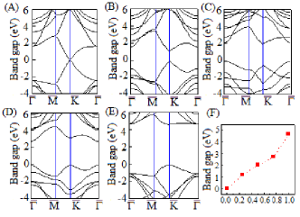
We firstly analyze the band structure of alloy . It is noticed that the B and N domain is impossible to be formed in the alloy due to the weaker binding energy of B-B and N-N bonds in the planar structure. Thus, we simply construct the alloy structure in unit cell ( and with symmetry group , with symmetry group ) and the band structures are calculated, as shown in Fig.4. The Fermi level is found to be not shifted and the two bands near the Dirac point is the major characteristic for the alloys. For the concentration of BN is 50 and 75, the band gap is indirect. With the concentration 50, the energy difference of , and are 2.058 eV, 2.24 eV and 2.48 eV, respectively. With the concentration 75, the transition energies of , , are 2.73 eV, 2.75 eV and 3.235 eV, respectively. The relation between band gap and concentration is almost linear with a small concavity around the concentration 75, as shown in Fig. 4F. Therefore, with alloying BN, the band structure can be modified effectively with the opened band gap. However, It is obvious that the ordered alloy with 2D planar structure is difficult to form, since BN just have small solubility in carbon materials.
With the thermodynamic process, it is possible that small amount of BN can be doped into the planar lattice of graphene. Due to the separation of phase, BN will precipitate and form the domain in the graphene. With the thermal catalytic CVD method, Ci have gained the hybrid h-BNC material with localized BN domains and graphene domainsc22 . By the development of material growth techniques, it is possible to obtain the graphene with small localized domain of BN. Now we considered what the shape of localized domains is. Since the binding energies of C-C and B-N bonds are larger than that of B-C and N-C bonds, the B-N and C-C bonds will tend to segregate and thus that the relative stable states will be with smaller amount of B-C and N-C bonds. With consideration of bond rule, the sum of the number of C-C, B-N, B-C and N-C is a constant. For the localized regions with different shapes and same areas, the domain with circle will have the smallest length of the boundary and thus the smallest number of B-C and N-C bonds. Therefore, the small domain of BN, (BN)3 and (BN)12 will be possible to exist in the graphene with the shapes which is shown in Fig. 5. In additional, it is possible that the doped graphene can be obtained by the combination of small pieces of graphene (such as ) and BN molecules (or , ) with chemical methods.
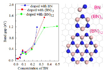
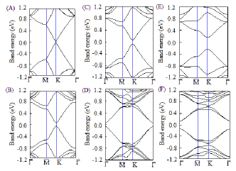
Here we demonstrate the electronic properties of doped graphene with small domain of BN, by calculating the doping of BN, (BN)3 and (BN)12 with different unit cell for the consideration of domain size and the concentration of dopants, as shown in Fig. 5 and Fig. 6. With the BN doping, the band gap is opened in the Dirac points and Fermi level is still around the Dirac points and not shifted. Due to the isoelectronic property of BN and C2, the codoping of B and N is similar with the alloying effect of BN as shown in Fig. 4 and the localized defect stats is not found in the band structure, as shown Fig.6. However, the change of band gap with the increase of concentration due to the doping of BN domains is not linear and there are two dips around the concentrations 0.04 and 0.12 in the curves of band gap vs. concentration. In the low concentration region, the charge of band gap due to the difference of domain size is small. This means the band gap in the Dirac points can be modulated effectively with the formation of small BN domain in the lattice of graphene with small concentration.
In Fig. 6 A and B, the band structure of graphene and that doped by BN molecule with unit cell is shown. It can be found that the bands of both structures match perfectly in the energy region [-0.4, 0.4] except the small region around the Dirac points. In the higher or lower energy region, the introduction of BN in lattice of graphene has broken the symmetry of band states and given an obvious perturbation to the eigenvalue of each state to make the small up- or down-shift for the energy. It is obvious that the conical dispersion is retained and the band departs from the linear dispersion asymptotically just around the Dirac points and thus opens a gap in the small region. With the increase of the concentration, the linear dispersion is modified in a relatively larger region of energy with a lager band gap. The phenomenon that bands around Dirac points are modulated is not changed obviously following the change of size of the small BN domains, as shown in Fig. 6 C, D, E and F. It is interesting that in the case of B or N doping with unit cell, the eigenstates around the Dirac points is obviously perturbed and the degenerated energies of and states are destroyed with zero band gap due to the symmetry break of the two sublattices. In the case of BN codoping, the degenerated energies of or states are not broken with an opened band gap. This may be due to the isoelectronic property of BN for C2 and the redistribution of charge in the region near the Dirac points.
III.3 Distribution of charge density and local potential of doped graphene
It is well known, with hybridization, the stable 2D hexagonal sheet is formed with the bonds. Obviously, the bond is strong can be contributed that the hybridized orbitals of the nearest-neighbour carbon atoms is superposed largely and thus makes the charges are mostly distributed in the region between two carbons. Duo to Pauli exclusion principle, the electron of the remnant orbitals will be distributed on the surface of network of bonds. This results that the electronic states of orbitals are sensitive to the local perturbations and the electrical properties of graphene is easy to be changed after the physical or chemical adsorption of gaps molecules due to the charge exchange and charge transfer. It is interesting that the electron charges of orbitals near the Dirac points are mostly distributed on the carbon atoms due to the electrons of mostly at the region between two carbons, as shown in Fig. 7 F. This is also the reason that the electronic states are put on the carbon atom in the theoretical model which is used to study the low-energy electronic properties near the Dirac points.
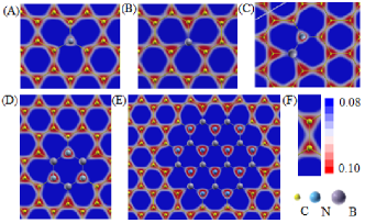
With the introduction of B, N or BN into the lattice of graphene, the charge distribution of bonds is not obviously changed. At the same time, the distribution of electrons is disturbed strongly. As Fig. 7 A shown, the charge of nitrogen near the Dirac point is localized and isolated and the charge of three neighbor carbons is reduced. It is obviously that some of charges of N atom is transferred into the electronic states of orbitals of carbon atoms and thus make the Fermi level up-shift. For B-doping, as shown in Fig. 7 B, the charge from other carbon has a trend to congregate to B atom because the B atom is less one electron than C atom. Thus, this makes the charge of three neighbor carbon atoms increased and the localized congregation of charge around boron atom makes the Fermi level down-shift. The projected charge distribution of doped graphene with BN molecule, (BN)3 and (BN)12 domains are demonstrated in Fig. 7 C, D and E, respectively. It is clear that the effect of B and N in the BN codoping to the neighbor carbon atoms is very similar to that of the isolated B- or N-doping. The effect of domain of BN to the carbon atoms of the sheet plane is localized. Due to isoelectronic property of BN and C2, the Fermi level is not shifted. Thus, the open of band gap may be attributed to the localized symmetry break of sublattices.
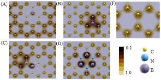
As shown in Fig. 8 F, the local potential in the plane paralleled to the sheet plane with a distance about 1.2Å reveals the reason that the charge near Dirac points localized on carbon atoms. With the B-doping shown in Fig. 8A, the B atom has a localized low potential and thus attracts the other electron from carbon atoms. The attraction is not enough that makes the redundant charge localized on B atom. However, this results in the redundant charge localized on three neighbor carbons. For the N-doing, as show in Fig. 8 B, the potential of three carbons near boron is lower. Thus, the charge of N atom has a trend to diffuse to the near carbon atoms. As shown Fig. 8 C and D, the introduction of BN domain in carbon lattice breaks the symmetry of potential which decides the distribution of charge near the Dirac points.
IV Conclusion
In summary, the effects of B-, N- and BN-doping or alloying to the electronic property has been studied by first-principles DFT calculations. It is found that the introduction of small BN domain in the lattice of graphene can be an effective method to open the band gap at the (or ) points. The modulation of gap is not sensitive to the size of BN domain and dependent on the concentration of BN. For B or N doping, it is found that the shift of Fermi level depends on the concentration of B or N. The doping of B or N can also open a gap in the Dirac points, while it is found that the single atom doping is not an effective method for engineering band structure of graphene. Furthermore, the band gap can not be opened when the graphene with unit cell is doped by B or N. This can be contributed that the perturbed potential result in the coupling of and states near Dirac points from and both which is folded to the gamma point. However, we can predict that the band gap of the actual sample with B or N doping should be opened due to the disorder effect of doping.
By analyzing the projected charge distribution, the surface charge which belongs to the states near the Dirac points is obviously disturbed and redistributed after the doping of B, N or BN domains, through the electronic states belong to the bands are not visually changed. The charge redistribution due to the doping is localized may be the reason that the energy states near Dirac points is just disturbed in the energy region [-0.4, 0.4] for the doping of BN domain. With the analysis of projected potential, the charge redistribution is considered to be a result of the small change of localized potential due to the doped defects. Thus, the band opening due to the doping of BN domain can be attributed to the breaking of localized symmetry. From the charge redistribution, we also suggest that the scattering from the doped defects may have not evident effect to the mobility of carriers in the graphene. With the doping of BN domain, we can obtain an effective band gap for the application of graphene on next-generation microelectronic devices.
References
- (1)
- (2) K. S. Novoselov, A. K. Geim, S. V. Morozov, D. Jiang, Y. Zhang, S. V. Dubonos, I. V. Grigorieva, and A. A. Firsov, Science 306, 666 (2004).
- (3) A. H. Castro Neto, F. Guinea, N. M. R. Peres, K. S. Novoselov, and A. K. Geim, Reviews of Modern Physics 81, 109 (2009).
- (4) A. K. Geim and K. S. Novoselov, Nature Materials 6, 183 (2007).
- (5) M. J. Allen, V. C. Tung, and R. B. Kaner, Chemical Reviews 110, 132 (2009).
- (6) S. V. Morozov, Phys. Rev. Lett. 97, 016801 (2006).
- (7) Y. Zhang, J. W. Tan, H. L. Stormer, and P. Kim, Nature 438, 201 (2005).
- (8) K. S. Novoselov, A. K. Geim, S. V. Morozov, D. Jiang, M. I. Katsnelson, I. V. Grigorieva, S. V. Dubonos, and A. A. Firsov, Nature 438, 197 (2005).
- (9) K. Novoselov, Nat Mater 6, 720 (2007).
- (10) P. Avouris, Z. H. Chen, and V. Perebeinos, Nature Nanotechnology 2, 605 (2007).
- (11) T. Ohta, A. Bostwick, T. Seyller, K. Horn, and E. Rotenberg, Science 313, 951 (2006).
- (12) S. Y. Zhou, G. H. Gweon, A. V. Fedorov, P. N. First, W. A. de Heer, D. H. Lee, F. Guinea, A. H. Castro Neto, and A. Lanzara, Nat Mater 6, 770 (2007).
- (13) M. Y. Han, Ouml, B. zyilmaz, Y. Zhang, and P. Kim, Physical Review Letters 98, 206805 (2007).
- (14) X. Peng and R. Ahuja, Nano Letters 8, 4464 (2008).
- (15) J. B. Oostinga, H. B. Heersche, X. Liu, A. F. Morpurgo, and L. M. K. Vandersypen, Nat Mater 7, 151 (2008).
- (16) D. W. Boukhvalov and M. I. Katsnelson, Physical Review B 78, 085413 (2008).
- (17) Y. Zhang, T.-T. Tang, C. Girit, Z. Hao, M. C. Martin, A. Zettl, M. F. Crommie, Y. R. Shen, and F. Wang, Nature 459, 820 (2009).
- (18) D. C. Elias, et al., Science 323, 610 (2009).
- (19) A. K. Singh, E. S. Penev, and B. I. Yakobson, ACS Nano 4, 3510 (2010).
- (20) G. Giovannetti, P. A. Khomyakov, G. Brocks, P. J. Kelly, and J. van den Brink, Physical Review B 76, 073103 (2007).
- (21) X.F. Fan, L. Liu, J.-L. Kuo, and Z.X. Shen, The Journal of Physical Chemistry C 114, 14939 (2010).
- (22) T. O. Wehling, K. S. Novoselov, S. V. Morozov, E. E. Vdovin, M. I. Katsnelson, A. K. Geim, and A. I. Lichtenstein, Nano Letters 8, 173 (2007).
- (23) L. Ci, et al., Nat Mater 9, 430 (2010).
- (24) A. Rubio, 9, 379 C380 (2010)
- (25) G. Kresse and J. Furthm ller, Computat. Mater. Sci. 6, 15 (1996).
- (26) G. Kresse and J. Furthm ller, Phys. Rev. B 54, 11169 (1996).
- (27) X. Wang, X. Li, L. Zhang, Y. Yoon, P. K. Weber, H. Wang, J. Guo, and H. Dai, Science 324, 768 (2009).