Quantum dot spectroscopy of proximity-induced superconductivity in a two-dimensional electron gas
Abstract
We report the realization of a hybrid superconductor-quantum dot device by means of top-down nanofabrication starting from a two dimensional electron gas in a InGaAs/InAlAs semiconductor heterostructure. The quantum dot is defined by electrostatic gates placed within the normal region of a planar Nb-InGaAs quantum well-Nb junction. Measurements in the regime of strong Coulomb blockade as well as cotunneling spectroscopy allow to directly probe the proximity-induced energy gap in a ballistic two-dimensional electron gas coupled to superconductors.
Hybrid devices in which a quantum dot (QD) is connected to superconducting (S) electrodes display a rich physical behavior, which stems from the coexistence of competing phenomena such as proximity superconductivity, Coulomb blockade and the Kondo effectDe Franceschi et al. (2010). Several examples of hybrid QD devices have been demonstrated so far, all of which rely on nanostructures defined by bottom-up approaches such as carbon nanotubesBuitelaar et al. (2002), semiconductor nanowiresSand-Jespersen (2007) and self-assembled QDsShibata et al. (2007); KatsarosG. et al. (2010). Transport studies in these nanosystems have demonstrated Josephson currents in S-QD-S devices and tuning of the critical current by changing the QD charge statevan Dam et al. (2006); Ingerslev Jorgensen (2007). Other authors have focused on quasiparticle transport, in particular on the interplay of Coulomb blockade, superconducting order in the leads and Kondo effectEichler (2007); Doh (2008).
In the perspective of practical implementations, large-scale integrability is a key requirement, and a top-down nanofabrication approach based on two dimensional electron gases (2DEGs) confined in semiconductor heterostructures would be preferable. Finally, QDs embedded into 2DEG-based hybrid structures can be used as a spectroscopic tool of proximity-induced superconductivity in ballistic electronic systems. While the local density of states (DOS) in proximized normal metal films has been probed using weakly-coupled tunnel contactsGueron et al. (1996); le Sueur et al. (2008), a similar measurement in the case of the 2DEG hosted in a ballistic semiconductor heterostructure has not been performed to date.
In this letter we report the realization of a hybrid S-QD-S device by means of top-down nanofabrication, starting from a 2DEG confined in a In0.80Ga0.20As/In0.75Al0.25As heterostructure. Following previous workref12 ; ref13 ; ref14 , the QD is formed by applying negative voltages to surface electrostatic gates placed on top of a narrow mesa strip etched in the heterostructure, and laterally contacted by superconducting niobium electrodes. We discuss the impact of the proximity-induced superconductivity on the transport properties in different regimes of coupling to the leads, and measure the proximity-induced energy gaps in the two-dimensional electron gas.
A scanning electron micrograph and the main nanofabrication steps are shown in Fig. 1(a,b). The active region of the heterostructure contains a -thick -doped In0.80Ga0.20As quantum wellref15 ; ref16 , sandwiched between In0.75Al0.25As barriers. The sheet electron density, measured from the period of Shubnikov - de Haas oscillations, is . The mobility is equivalent to an electron mean free path . InAs and InxGa1-xAs alloys with high molar fraction have often been used in association with Nb for the realization of hybrid ballistic devices, thanks to their property of forming Schottky barrier-free junctions. For the same reason a suitable dielectric is required for the electrical insulation of the electrostatic gates.
The nanofabrication of the hybrid device requires several mutually-aligned steps of electron beam lithography (EBL). First [Fig. 1(a1)] we pattern a dielectric strip on the heterostructure surface, by means of EBL, using hydrogen silsesquioxane (HSQ) as a negative tone e-beam resistLauvernier et al. (2004). Thickness and width of the strip are and , respectively. The mesa strip is defined by wet etching in a H3PO4-H2O2 solution through an EBL-patterned poly(methyl methacrylate) mask (a2). Electrostatic gates are then added by thermal evaporation and liftoff (a3), followed by sputtering and liftoff of the Nb side contacts (a4). The junction has a width , while the inter-electrode distance, equal to the width of the etched mesa strip, is . In order to maximize interface transmissivity, the native oxide and possible contaminants must be removed from the mesa sidewalls before the deposition of the contacts. To this end we perform low-energy Ar+ sputter-cleaning in high vacuum, immediately before the deposition of Nbref18 , ref18.1 .
Low temperature measurements are performed down to . Below the critical temperature of the Nb films, proximity-induced superconductivityPannetier and Courtois in the semiconductor modifies the DOS at energies (where is the superconducting gap of the Nb films and the Boltzmann constant). The normal-state resistance of the junction is , roughly two times larger than the lower bound set by the Sharvin resistance , where is Planck’s constant. The voltage-current characteristicref18.6 of the open junction (all gates set to ground), measured at , is plotted in Fig. 1(c) and shows a switching current . We note that in this configuration the junction length is smaller than the electron scattering length and larger than the induced coherence length (where is the electron effective mass in In0.80Ga0.20As), so that the normal region is ballistic and the junction falls in the intermediate length regime.
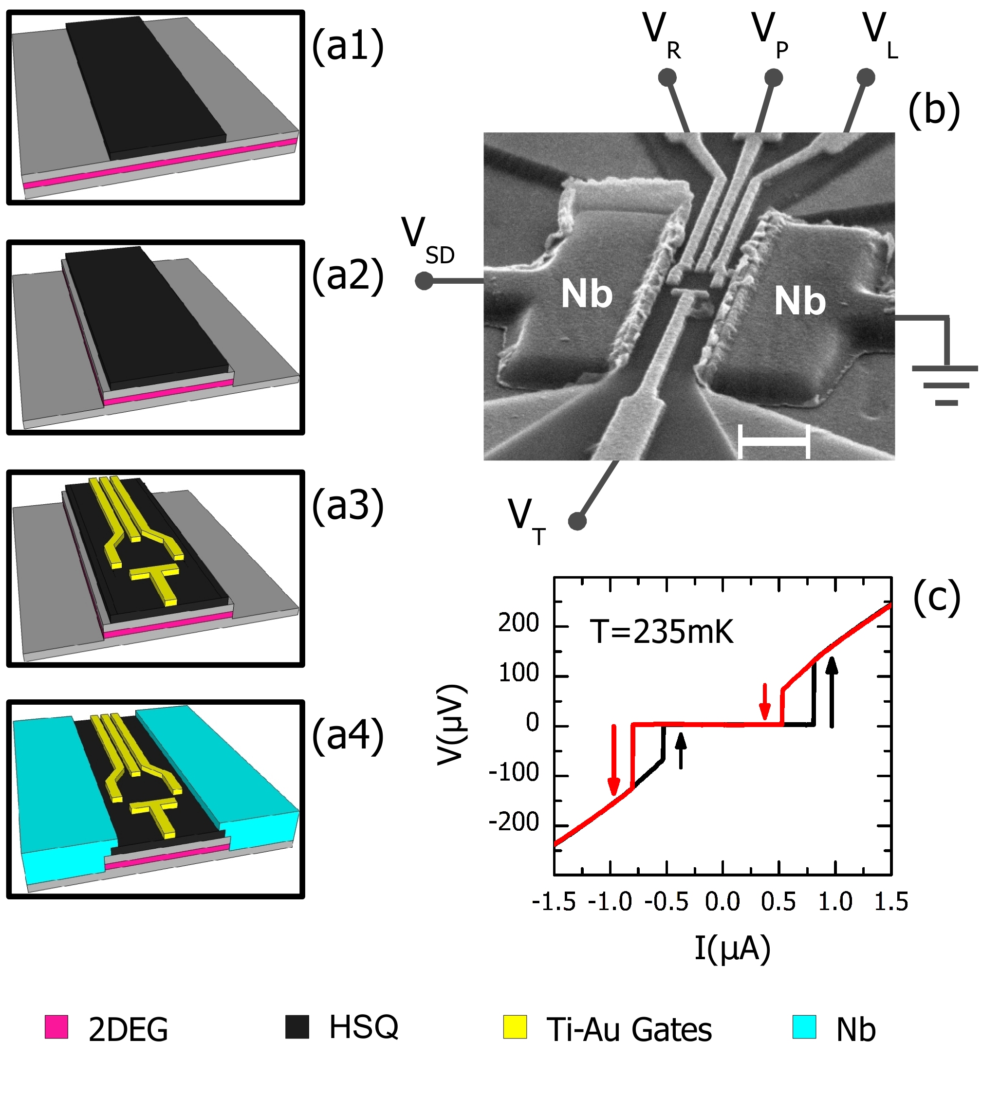
When negative voltages , and are applied to the electrostatic gates [see Fig. 1(b)], the underlying 2DEG regions are depleted, forming a QD. The voltage applied to the fourth gate allows to tune the charge state of the QD. Two point-contacts with tunable transparency couple the QD island to the nearby Nb-InGaAs (S-2DEG) junctions. The distance between the Nb-InGaAs interfaces and the electrostatic gates that define the QD is of the order of , below the induced coherence length . For superconductor-normal metal (SN) junctions with a normal region length approaching or smaller than the proximity-induced energy gap is expected to increase, reaching in the case of ideal NS interfaces in the short junction limit; a suppression of should occur for contacts with finite interface transparencyHammer et al. (2007). It is known that the stability diagram of a QD directly connected to superconductors reveals the presence of a gap in the DOS, both for weak and strong tunnel coupling to the leadsShibata et al. (2007); Doh (2008); Yeyati et al. (1997). We will show in the following that our device can be easily tuned between the two regimes, and report our measurement of in the 2DEG.
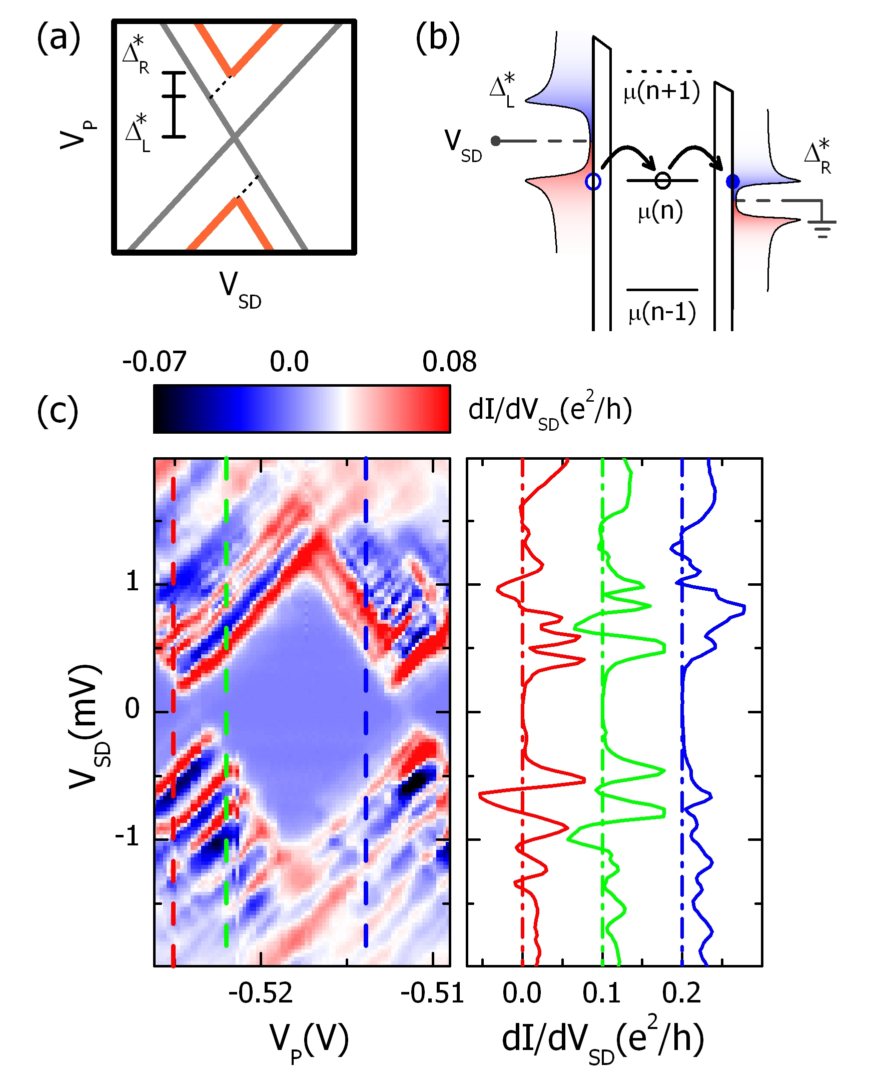
Figure 2(a) shows measurements () in a regime of weak QD-lead coupling: the QD differential conductance is plotted in color scale as a function of the source-drain bias and (stability plot). In the diamond-shaped regions of low conductance electron tunneling through the QD is forbidden by Coulomb repulsion, and the QD occupation number is constant. Diamond edges with positive (negative) slope correspond to the onset of single electron tunneling from the left (right) lead. A sketch of the stability plot is given in Fig. 2(b): in the case of normal contacts (gray lines) the diamond edges cross at , forming zero bias Coulomb blockade peaks at the charge-degeneracy points. The presence of gaps and in the DOS of the left and right lead, respectively, shifts the onset of the corresponding diamond edges [orange lines in Fig. 2(b)] to higher values of [see Fig. 2(c)]. The measured values of and are and . Such a large asymmetry could be linked to asymmetric tunnel coupling of the QD to the leads and to the consequent asymmetric depletion and weakening of the proximity effect in the adjacent 2DEG regions. Our finding that is also consistent with the fact that excited-state lines pertaining to the left lead are more intense and followed by regions of large negative Doh (2008).
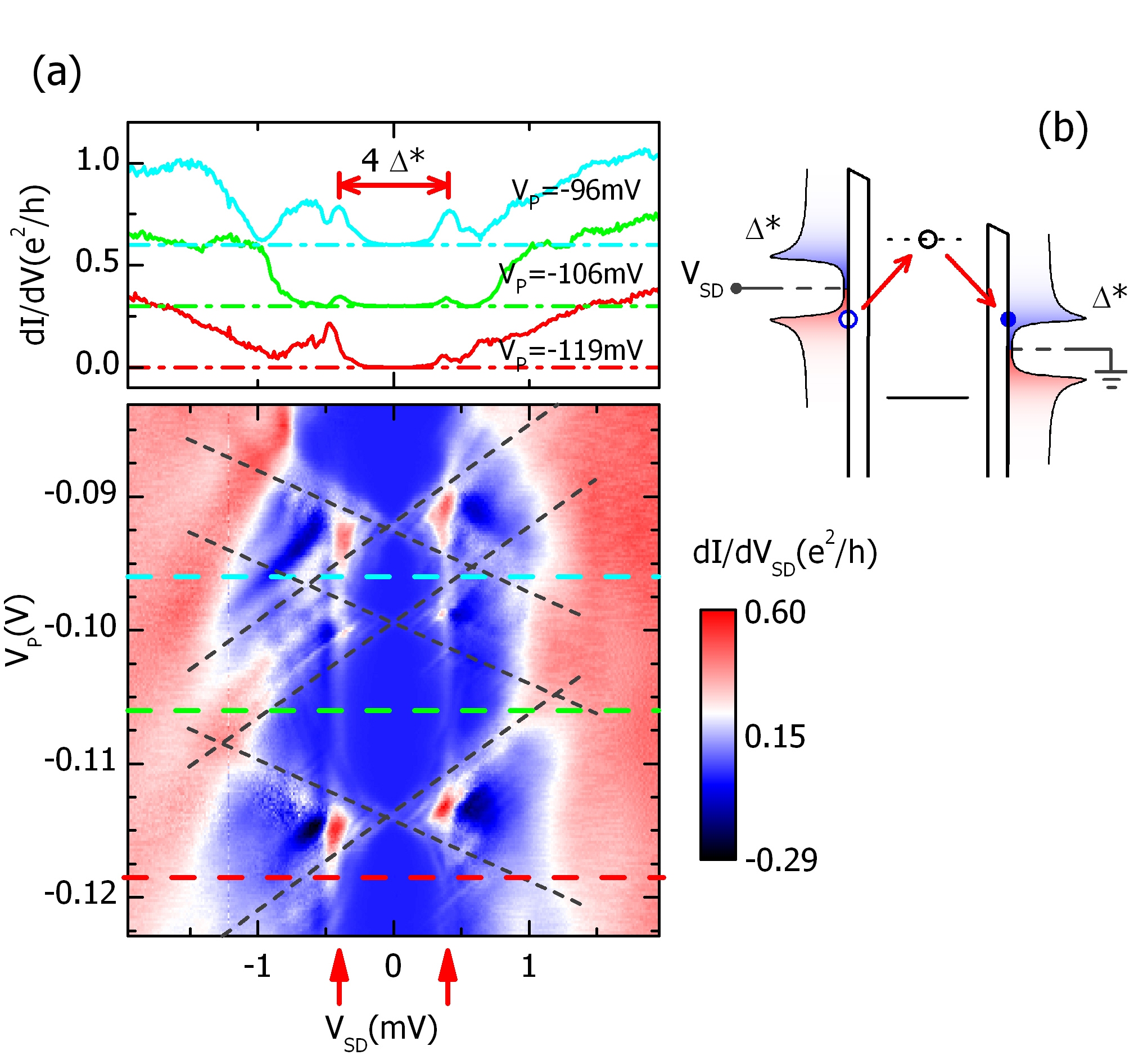
Our device architecture allows to easily tune the QD to a regime of stronger coupling to the leads by increasing the voltages , , of a few . In this regime cotunneling processes lead to the appearance of finite conductance inside the Coulomb diamonds [see Fig. 3(a)]]. Symmetric peaks in located at a constant voltage , independent of the charge state of the QD, are due to elastic cotunneling processes, such as the one sketched Fig. 3(b). In the upper panel of Fig. 3(a) the differential conductance is plotted versus for constant values of indicated by the dashed lines of corresponding color in the lower panel. In this case our data indicate that : the onset of elastic cotunneling takes place at , where the particle- and hole-like DOS peaks in the two leads are aligned. We thus find . This value is slightly smaller than the value of found in the weak coupling regime (the difference being comparable with the uncertainty on ). We note that the data shown in Fig. 2 and Fig. 3 were taken in different cooldowns of the device, and a fluctuation in could explain a variation in the strength of the proximity effect.
In conclusion, we demonstrated a hybrid QD device obtained by means of standard top-down nanofabrication, which combines a Nb-In0.8Ga0.2As-Nb planar junction with a lateral QD confined by electrostatic gates. Transport measurements allow to directly measure a proximity-induced gap in the 2DEG which results of the order of . As these results are relevant to the development of non-dissipative single electron transistors, further work will be devoted to the study of Josephson coupling through our device.
The authors would like to thank P. Spathis for fruitful discussions and for help with the cryogenic setup. We acknowledge partial financial support from the E.U. Project HYSWITCH (grant No. FP6-517567), the MIUR-FIRB No. RBIN06JB4C, the INFM-CNR Seed project ‘Quantum dot refrigeration: accessing the regime in solid-state nanosystems’, and the NanoSciERA project ‘NanoFridge’.
References
- De Franceschi et al. (2010) S. De Franceschi, L. Kouwenhoven, C. Schönenberger, and W. Wernsdorfer, Nat. Nano. 5, 703 (2010).
- Buitelaar et al. (2002) M. R. Buitelaar, T. Nussbaumer, and C. Schönenberger, Phys. Rev. Lett. 89, 256801 (2002).
- Sand-Jespersen (2007) T. Sand-Jespersen, J. Paaske, B. M. Andersen, K. Grove-Rasmussen, H. I. Jørgensen, M. Aagesen, C. B. Sørensen, P. E. Lindelof, K. Flensberg, J. Nygård, Phys. Rev. Lett. 99, 126603 (2007).
- Shibata et al. (2007) K. Shibata, C. Buizert, A. Oiwa, K. Hirakawa, and S. Tarucha, Appl. Phys. Lett. 91, 112102 (2007).
- KatsarosG. et al. (2010) G. Katsaros, P. Spathis, M. Stoffel, F. Fournel, M. Mongillo, V. Bouchiat, F. Lefloch, A. Rastelli, O. G. Schmidt, S. De Franceschi, Nat. Nano. 5, 458 (2010).
- van Dam et al. (2006) J. A. van Dam, Y. V. Nazarov, E. P. Bakkers, S. De Franceschi, and L. P. Kouwenhoven, Nature 442, 667 (2006).
- Ingerslev Jorgensen (2007) H. Ingerslev Jorgensen, T. Novotny, K. Grove-Rasmussen, K. Flensberg, and P. Lindelof, Nano Lett. 7, 2441 (2007).
- Eichler (2007) A. Eichler, M. Weiss, S. Oberholzer, C. Schönenberger, A. Levy-Yeyati, J. C. Cuevas, A. Martín-Rodero, Phys. Rev. Lett. 99, 126602 (2007).
- Doh (2008) Y.J. Doh, S. De Franceschi, E. Bakkers, and L. P. Kouwenhoven, Nano Lett. 8, 4098 (2008).
- Gueron et al. (1996) S. Gueron, H. Pothier, N.O. Birge, D. Esteve and M.H. Devoret, Phys. Rev. Lett. 77, 3025 (1996).
- le Sueur et al. (2008) H. le Sueur, P. Joyez, H. Pothier, C. Urbina, and D. Esteve, Phys. Rev. Lett. 100, 197002 (2008).
- (12) H. Takayanagi, T. Akazaki, J. Nitta, Phys. Rev. Lett. 75, 3533 (1995).
- (13) T. Bauch, E. Hürfeld, V. M. Krasnov, P. Delsing, H. Takayanagi, T. Akazaki, Phys. Rev. B 71, 174502 (2005).
- (14) F. Deon, V. Pellegrini, F. Carillo, F. Giazotto, G. Biasiol, L. Sorba, F. Beltram, Appl. Phys. Lett. 96, 142107 (2010).
- (15) F. Capotondi, G. Biasiol, D. Ercolani, V. Grillo, E. Carlino, F. Romanato, and L. Sorba, Thin Solid Films 448, 400 (2005).
- (16) W. Desrat, F. Giazotto, V. Pellegrini, F. Beltram, F. Capotondi, G. Biasiol, and L. Sorba, Phys. Rev. B 69, 245324 (2004).
- Lauvernier et al. (2004) D. Lauvernier, J. P. Vilcot, M. François, and D. Decoster, Microelectr. Eng. 75, 177 (2004).
- (18) F. Giazotto, K. Grove-Rasmussen, R. Fazio, F. Beltram, E. H. Linfield, and D. A. Ritchie, J. of Supercond. 17, 317 (2004).
- (19) The Fermi wavevector mismatch between Nb and the 2DEG also negatively affects interface transparency..
- (20) B. Pannetier and H. Courtois, J. of Low Temp. Phys. 118, 599 (2000).
- (21) The observed hysteresis is typical of S-N-S proximity junctions with high critical current densityref19 .
- (22) H. Courtois, M. Meschke, J. Peltonen, and J. Pekola, Phys. Rev. Lett. 101, 057005 (2008).
- Hammer et al. (2007) J.C. Hammer, J.C. Cuevas, F.S. Bergeret, and W. Belzig, Phys. Rev. B 76, 064514 (2007).
- Yeyati et al. (1997) A.L. Yeyati, J.C. Cuevas, A. Lopez-Davalos, A. Martín-Rodero, Phys. Rev. B 55, R6137 (1997).