Quantum Andreev effect in 2D HgTe/CdTe quantum well-superconductor systems
Abstract
The Andreev reflection (AR) in 2D HgTe/CdTe quantum well-superconductor hybrid systems is studied. A quantized AR with AR coefficient equal to one is predicted, which is due to the multi-Andreev reflection near the interface of the hybrid system. Importantly, this quantized AR is not only universal, i.e., independent of any system parameters and quality of the coupling of the hybrid system, it is also robust against disorder as well. As a result of this quantum Andreev effect, the conductance exhibits a quantized plateau when the external bias is less the superconductor gap.
pacs:
74.45.+c, 85.75.-d, 73.23.-bRecently, the topological insulator (TI), a new state of matter, has attracted a lot of theoretical and experimental attention.ref1 ; ref2 ; ref3 ; ref4 ; ref5 ; ref6 ; ref7 ; ref8 The TI has an insulating energy gap in the bulk states, but it has exotic gapless metallic states on its edges or surfaces. The TI is first predicted in two-dimensional (2D) systems, e.g. the graphene and HgTe/CdTe quantum well (QW).ref2 ; ref3 The 2D TI has the gapless helical edge states and exhibits the quantum spin Hall effect. This helical edge states, with the opposite spins on a given edge or opposite edges for a given spin direction containing opposite propagation directions, are topologically protected and are robust against all time-reversal-invariant impurities. Soon after that, people also found the TI in three-dimensional (3D) materials, e.g., , , etc.ref4 ; ref5 On the experimental side, the TI in HgTe/CdTe QW, , , and so on, have been successfully confirmed.ref4 ; ref6 ; ref7
The Andreev reflection (AR) which was found about fifty years ago is an important transport process.ref9 The AR occurs near the interface of a conductor and a superconductor, in which an incident electron from the metallic side is reflected as a hole and a Cooper pair is created in the superconductor. When the bias is smaller than the superconductor gap, the conductance of the conductor-superconductor hybrid device is mainly determined by the AR.aref1 For a perfect conductor-superconductor interface, the probability of the AR can reach one. However, the AR coefficient is usually very small due to various scattering mechanisms such as the contact potential of the interface, the impurities, the mismatch of the density of states of the conductor and superconductor, and so on. Although the AR has been extensively investigated in various conductor-superconductor hybrid systems, up to now, people has not observed a robust quantized AR that holds for various system parameters and sustains in the presence of a variety of scattering mechanisms.
In this letter, we study the AR in a 2D TI-superconductor (TI-S) hybrid system. We found that in this system the AR is quantized with AR coefficient being one, because of the multi-Andreev reflection along the TI-S interface. Importantly, this quantized AR is universal and robust. The quantization of AR persists regardless of the system parameters such as the Fermi energy, energy of the incident electron and the size of the system. It is also robust against the presence of impurities and contact potential of the interface. Due to the quantum Andreev effect, the conductance exhibits the plateau with the plateau value being () for the two-terminal (four-terminal) TI-S hybrid system.
Since the TI phase in HgTe/CdTe QW has been experimentally realized,ref6 ; ref7 we shall focus on the HgTe/CdTe QW in the following calculation. The results will be the same for other 2D TI systems. We consider two HgTe/CdTe QW-superconductor hybrid devices as shown in Fig.1(f): one is a ribbon of HgTe/CdTe QW coupled to a semi-infinite superconducting lead which is referred as the two-terminal device and the other is a cross of HgTe/CdTe QW coupled to a superconducting lead which is referred as the four-terminal device. The advantage of the four-terminal device is that the ”trajectories” of the incident electron and reflected hole can be clearly shown.
The hybrid devices are described by the Hamiltonian , where , , and are the Hamiltonian of the HgTe/CdTe QW, superconducting lead, and the coupling between them, respectively. By discretizing spatial coordinates of the continuous effective Hamiltonian in Ref.ref3, and using the Nambu representation, the Hamiltonian is given by:ref11
| (1) |
where is the site index, and are unit vectors along and directions, , and are annihilation operators of electron on the site at the states , , , and . In Eq.(1), are the matrix Hamiltonian, where , , and , with , , . Here is the Fermi energy (pinned by superconductor condensate), is the lattice constant, and , , , , and are the system’s parameters which can be experimentally controlled. The Hamiltonian of the superconducting lead is: where is the superconductor gap and () is the creation (annihilation) operators in the superconducting lead with the momentum . Here we consider the general s-wave superconductor. The coupling Hamiltonian is: , where the operator and Here the parameters and are the coupling strengths between the superconductor and HgTe/CdTe QW, which depends on the interface’s contact potential and the quality of the coupling in the experiment.
By using the Green’s functions, the charge current and spin current from the n-th terminal of the HgTe/CdTe QW flowing into the device are and , whereref12
| (2) | |||||
Here for , , and , with being the Fermi distribution function and being the voltage of the terminal-n. In Eq.(2), and are respectively the normal transmission coefficient from the terminal-n to the terminal-m and to the superconductor terminal, and is the AR coefficient with the incident electron from the terminal-n and the reflected hole going to the terminal-m. The linewidth function and the Green’s functions can be calculated from , where is the Hamiltonian of the scattering region as shown in Fig.1f (dotted region). The self-energy functions and due to terminals of the TI and superconducting lead can be calculated as in Ref.[ref12, ; ref13, ; ref14, ]. In the following numerical calculations, we choose the parameters from the realistic materials:ref6 (1) the HgTe/CdTe QW’s parameters are , , , and . (2) the superconductor’s parameters are the gap energy . The lattice constant is set to and the TI-S coupling strengths are taken .
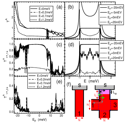
We first study the two-terminal system. Due to the time-reversal symmetry and the symmetry around the y axis, the AR coefficients have the properties and . Fig.1a and 1b show the AR coefficient versus the Fermi energy and energy of the incident electron. Now the parameter is set so that the HgTe/CdTe QW is in the TI phase.ref3 Fig.1a and 1b clearly show that exhibits a plateau with the plateau value equal to one as long as is in the bulk gap of TI and the energy within the superconductor gap . Since there is only one transmission channel (i.e. the edge state) when is in the bulk gap, means that the incident electron is completely Andreev reflected. It is remarkable that the quantum Andreev effect occurs in such a wide range of and , while in all previous metal-superconductor hybrid systems the resonant condition occurs only at certain set of parameters. Fig.1a also shows that when is out of the bulk gap, there is no plateau in the AR coefficient and depends on both and . For , can be larger than one (see Fig.1a) because there are many transmission channels. However, the AR coefficient for each transmission channel is still much smaller than one.
In order to reveal the nature of quantum Andreev effect, we will study the four-terminal device. In the four-terminal device, the AR coefficient has elements, so the trajectories of the incident electron and reflected hole can clearly be shown. When the HgTe/CdTe QW is in the TI regime, only is nonzero and other eight elements are zero. In particular, as soon as the energy and , the quantized plateau with emerges and this plateau is independent of and (see Fig.1c and 1d). These results can be understood with the help of helical edge states, in which the spin-up and spin-down carriers move along the edge of the HgTe/CdTe QW in clockwise and counter-clockwise directions, respectively.ref1 ; ref3 We consider the case of the spin-up electron coming from the terminal-1 when the energy . As shown in Fig.1f, two reflection processes occur at the TI-S interface: (1). it can be Andreev reflected back as a spin-down hole to the same terminal which will contribute to . (2). It can also be normal reflected as an electron (spin up) along the TI-S interface, eventually to terminal-3. Note that the normal reflection as an electron back to the terminal-1 is prohibited by the time-reversal invariance and the helical edge states being a pair of Kramer states. The reflected electron traveling to terminal-3 has to go along the TI-S interface since the only available transmission channel is the edge state. This results in a reflection again at the TI-S interface where part of the electron is Andreev reflected as the hole back to terminal-1 and the rest is normal reflected as electron towards terminal-3. As this continues, multi-reflections occur as normal electron traverses along the TI-S interface and eventually the transmission probability becomes zero if the TI-S interface is long enough. Clearly, it is this multi-AR that gives rise to the quantum Andreev effect with the quantized AR . Furthermore, we have three observations: (i) If the energy , all AR coefficients decrease as usual (see Fig.1d),ref15 because of the occurrence of the normal tunneling from TI to the superconductor. (ii) When is out of the bulk gap, all AR coefficients have the same behavior: AR coefficient for each transmission channel is in general small and strongly depends on and (see Fig.1c, 1d, and 1e). (iii) For the spin-down incident carrier, it is easy to show that has the quantized plateau similar to .
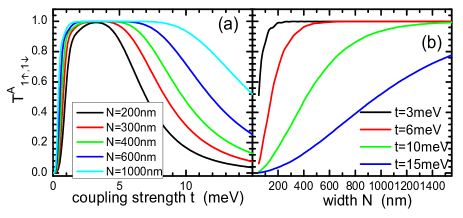
Next, we study how the quantized AR is affected by the system parameters. Fig.2 shows the AR coefficient versus the width of the HgTe/CdTe QW ribbon and the coupling strength . The results show that the quantization of AR persists for a broad range of the coupling strength . In addition, the wider the width , the broader the quantization plateau is. For , the AR quantization plateau can sustain when varies nearly one order of magnitude. Finally, with the increase of the width , the AR coefficient rises monotonously before it reaches quantized value due to the fact that the incident electron has more chance of multi-AR for the longer TI-S interface. These results show the universal feature of the quantum Andreev effect: it is independent of the system parameters.
This universal feature can also be understood analytically from multi-AR along the interface of TI and superconductor. Due to the nature of TI the incoming spin up electron can be Andreev reflected as spin down hole with AR amplitude and normal reflected as a spin up electron with reflection amplitude . Note that and , respectively, play the role of reflection and transmission amplitudes for normal system. Clearly, the normal reflection amplitude that plays the role of transmission coefficient for normal system will vanish after successive ARs for large . While for a particular AR and depend on system parameters such as , incoming electron energy, and coupling strength , it is the multi-AR that makes the quantum Andreev effect independent of system parameters.
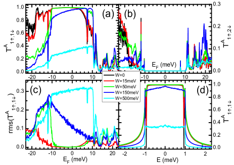
Is the quantized AR robust against the disorder? To answer this question, we consider the on-site Anderson disorder in a region near the TI-S interface (see the light gray (red) region in Fig.1f). Because of the disorder, an extra on-site term is added on each site in the disorder region, where is the diagonal matrix with diagonal elements (). is assumed uniformly distributed in the range with the disorder strength . Fig.3 shows the AR coefficients and its fluctuation versus and . The results show that the quantized AR plateau in is very robust: the AR plateau can persist and its fluctuation is zero for the disorder strength up to because of the helical edge states being very robust. Upon further increasing of from , starts to decrease and the fluctuation becomes nonzero because at large disorders the system reaches the diffusive regime and the helical edge states are destroyed. Hence, as long as the edge state is survived, disorder has no effect on the quantum Andreev effect.

Let us investigate the conductance () and spin conductance (). We set the biases of the HgTe/CdTe QW terminals, , and the superconductor-terminal bias . Fig.4a shows the conductance and spin conductance versus the bias for the four-terminal system. When is inside the bulk gap, (in the unit ) is exactly equal to (in the unit ) since only the spin-up electron traverses from the terminal-1 to the TI-S interface with the spin-down hole Andreev reflected back. In particular, when , a (spin) conductance plateau emerges with the plateau value () because of the quantized AR with . Here we emphasize that like the quantized AR this conductance plateau is also universal (i.e. it is independent of the system parameters and the quality of TI-S coupling) and robust against the disorder. Since the TI phase in HgTe/CdTe QW has been realized experimentally,ref6 ; ref7 this predicted quantum Andreev effect with quantized conductance plateau should not be difficult to observe using the present technology. On the other hand, when is out of the bulk gap, both and are not equal and they are sensitive to the system parameters. Finally, we comment on following two points: (i) If HgTe/CdTe QW is in the normal state (i.e. ), no plateau emerges for both the AR coefficient and conductance (see Fig.4c and 4d), similar to the ordinary conductor-superconductor hybrid system. (ii). For the two-terminal device with the HgTe/CdTe QW in TI regime, the conductance also exhibits the quantum Andreev effect with quantized AR conductance at (see Fig.4b). However, the spin conductance is exactly zero due to the fact that the left and right edges of the HgTe/CdTe QW ribbon carry the same current but opposite spin current.
In summary, we predict a quantum Andreev effect in the 2D TI-S hybrid system, in which the AR coefficient is quantized with the value one. Importantly, the quantized AR plateau is independent of various system parameters and the quality of TI-S coupling, and it also is robust against the disorders. Hence it should be easy to observe it using the present technology. Due to the quantized AR, the conductance also exhibits the same quantized plateau when the bias is within the superconductor gap.
Acknowledgments: This work was financially supported by NSFC under Grant Nos. 10974236, 10974043, and 11074174, and a RGC Grant (No. HKU 704308P) from the gov. of HKSAR.
References
- (1) J.M. Moore, Nature 464, 104 (2010).
- (2) C.L. Kane and E.J. Mele, Phys. Rev. Lett. 95, 146802(2005); 95, 226801(2005).
- (3) B.A. Bernevig et al, Science 314, 1757 (2006).
- (4) D. Hsieh, et al., Nature(London) 452, 970 (2008); 460, 1101 (2009); Y.L. Chen, et al., Science 178, (2009); T. Zhang, et al., Phys. Rev. Lett. 103, 266803 (2009).
- (5) L. Fu et al, Phys. Rev. Lett. 98, 106803 (2007); H. Zhang, et al., Nat. Phys. 5, 438 (2009).
- (6) M. Knig, et al., Science 318, 766 (2007); J. Phys. Soc. Jpn. 77, 031007 (2008).
- (7) A. Roth, et al., Science 325, 294 (2009).
- (8) H. Jiang, et al., Phys. Rev. Lett. 103, 036803 (2009); Q.-F. Sun and X.C. Xie, ibid. 104, 066805 (2010).
- (9) A. F. Andreev, Sov. Phys. JETP 19, 1228 (1964).
- (10) K. Kang, Phys. Rev. B 57, 11891 (1998); Physica E 5, 36 (1999).
- (11) H. Jiang, et al., Phys. Rev. B 80, 165316 (2009).
- (12) Q.-F. Sun and X.C. Xie, J. Phys.: Condens. Matter 21, 344204 (2009); S.-G. Cheng, et al., Phys. Rev. Lett. 103, 167003 (2009).
- (13) M.P. Lopez Sancho, et al., J. Phys. F: Met. Phys. 14, 1205 (1984); 15, 851 (1985).
- (14) Q.-F. Sun et al, Phys. Rev. B 59, 3831 (1999); 59, 13126 (1999).
- (15) G.E. Blonder et al, Phys. Rev. B 25, 4515 (1982).