Phonon Transport in Suspended Single Layer Graphene
Abstract
We report the first temperature dependent phonon transport measurements in suspended Cu-CVD single layer graphene (SLG) from 15K to 380K using microfabricated suspended devices. The thermal conductance per unit cross section /A increases with temperature and exhibits a peak near 280K (10K) due to the Umklapp process. At low temperatures (140K), the temperature dependent thermal conductivity scales as 1.5, suggesting that the main contribution to thermal conductance arises from flexural acoustic (ZA) phonons in suspended SLG. The /A reaches a high value of 1.7105 W/m2K, which is approaching the expected ballistic phonon thermal conductance for two-dimensional graphene sheets. Our results not only clarify the ambiguity in the thermal conductance, but also demonstrate the potential of Cu-CVD graphene for heat related applications.
pacs:
65.80.Ck, 63.22.Rc, 81.05.ue, 81.07.-bHeat conduction in low-dimensional systems has been extensively studied in past decades because of its importance in understanding the microscopic mechanism of thermal transport phenomena, and its potential applications in manipulating and controlling heat flow lowD . Although significant progress has been made for one-dimensional systems lowD , the study of heat conduction in two-dimensional (2D) systems is still in its infancy due to the lack of proper materials. The discovery of graphene has changed this scenario graphene ; neto . It not only provides us with an ideal platform for thermal transport studies in 2D systems, but also opens the door for many novel heat related applications pop . However, difficulties in integrating graphene sheets with device structures needed for measuring intrinsic thermal properties have resulted in experiments which only offer partial answers. Pioneering Raman based measurements at room temperature have indicated exceptional high thermal conductivity in graphene balandin1 ; balandin2 ; balandin3 , far exceeding that of diamond diamond and carbon nanotubes Nanotube ; CNT . However, recent measurements have shown that these values can easily vary by one order of magnitude from 600 W/mK to 5300 W/mK balandin2 ; Geim ; Ruoff . Efforts to develop traditional suspended microfabricated heater wires have been only successful by compromising on the SiO2 substrate, resulting in significant phonon leakage into the substrate and strong interfacial scattering between graphene and the underlying substrate LSScience . Therefore, the temperature dependent thermal conductivity () needs to be investigated in suspended graphene. This will be the key in understanding the 2D nature of phonons in graphene and is crucial in identifying which phonon branch dominating the heat conduction.
In this Letter, we present the first temperature dependent thermal transport measurements in a suspended single layer graphene (SLG) sheet in the temperature range from 15K to 380K. Our approach takes advantage of the recent progress in wafer-scale graphene growth by the Cu-based chemical vapor deposition (Cu-CVD) method CVDruoff ; CVDKorea . The thermal conductivity follows a 1.5 power law, demonstrating that most of the heat in free standing graphene is carried by flexural acoustic (ZA) phonons. At room temperature, the thermal conductance per unit cross section /A in Cu-CVD graphene reaches a high value of 3.8108 W/m2K. Below 140K, this high value is found to be approaching the theoretical ballistic limit in graphene sheets ballisticMingo ; ballisticNL .
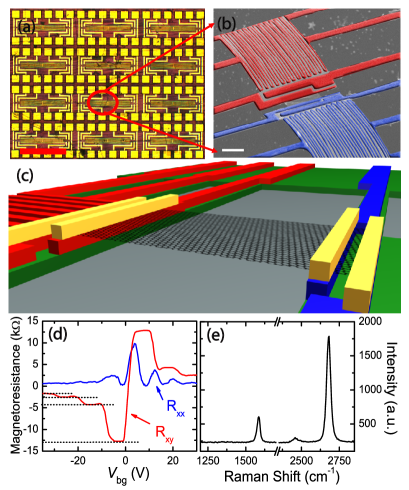
We employed typical prepatterned suspended heater wires to measure the thermal conductance and thermal power in suspended single layer graphene. Similar methods have been used to study thermal transport in carbon nanotubes Nanotube ; Nanotube2 and nanowire Nanowire . The structures were fabricated on silicon nitride (SiNx)/Si multilayer wafers and the fabrication details have already been discussed by Shi . JHT . The transfer of exfoliated graphene onto such fragile structures is difficult and remains very challenging. Fortunately, the recent progress in Cu-CVD graphene allows us to overcome many of these challenges by the sheer number of available junctions on a single chip. The growth of SLG by Cu-CVD method is described elsewhere in detail CVDKorea . The outstanding electronic properties and sub-100 micrometers grain size grainsize suggest that the physical properties of Cu-CVD graphene are comparable to that of exfoliated graphene. Graphene films were transferred onto these prepatterned structures before suspending them (Figure 1a) supplementary . They were then patterned into micrometer-size rectangular structures by standard e-beam lithography, followed by an O2 plasma. In a second lithography step, 30nm Cr/Au bars were deposited on both ends of graphene to ensure good thermal contact with the Pt electrodes underneath graphene (Figure 1c). These Cr/Au bars also securely clamp graphene onto the Pt electrodes during the subsequent fabricating steps. After suspending graphene by etching in KOH, the devices were dried using a critical point dryer to avoid damage due to surface tension.
The scanning electron microscope image of a typical microfabricated device is shown in Figure 1b. The suspended device consists of two 2520 m2 SiNx membranes, each of which is supported by six 400m-long, 0.3m-thick and 1.5m-wide suspended SiNx beams. A 60nm-thick platinum resistor coil is deposited on top of each SiNx membrane. Since the resistance of the Pt resistors changes with temperature, they can serve as both heater (Rh) and temperature sensor (Rs). The suspended graphene (grey sheet in the middle of Figure 1b) bridges the two SiNx membranes and is electrically isolated from the Pt coils. In total, three samples from two separate Cu-CVD growth runs have been measured. Here we discuss representative data based on one graphene sheet, which is patterned to a width of 3m and a suspended length of 500nm. Since there is no back gate for such suspended graphene samples (etch depth200m), we could neither vary the carrier density nor calculate the mobility. However, this is not a severe limitation in our measurements due to the following reasons: a) thermal conductance in graphene is weakly dependent on carrier density; b) we can set the Fermi level near Dirac point by - annealing in vacuum suspended ; c) the sample quality can be investigated by characterizing the same batch of graphene on SiO2. The measured mobility is approximately 7700cm-2/Vs at =2K, which is comparable to that in exfoliated graphene. The half-integer quantum Hall measurements at =2K and =9T (Figure 1d) and Raman measurements (Figure 1e) also indicate high quality of our graphene samples.
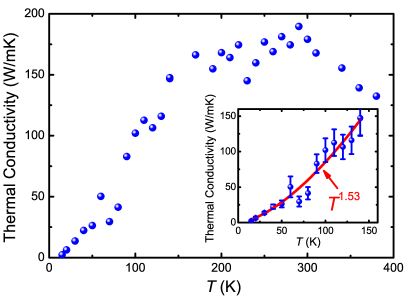
We now turn to the experimental results and discuss first the temperature dependent thermal conductivity (). Figure 2 shows the thermal conductivity in the temperature range from 15K to 380K of the suspended sample G1. is extracted from LA, where L is the sample length, A is the cross section area of graphene and is the measured thermal conductance of graphene supplementary . The observed increases by two orders of magnitude as the temperature increases, reaches a maximum of 190 W/mK at 280K(10K) and decreases at higher temperature. The most important result is the low temperature behavior of . The inset of Figure 2 shows that can be fitted by b. Here, b is the fitting parameter and is found to be 1.53(0.18). Theoretical work has predicted that the thermal conductivity in graphene yields a power law of , where varies from 1 for one-dimensional nanoribbons to 1.5 for two-dimensional graphene sheets ballisticNL . It is worth noting that this power law at low temperatures was not observed in supported graphene LSScience . Our measurements of the law directly reveals for the first time unambiguously intrinsic phonon transport in graphene sheets.
We shall now interpret the physics behind the observed (). The acoustic vibrations in 2D graphene lattice are composed of two types of phonons: in-plane phonons (TA and LA phonons) with linear dispersion, and out-of-plane phonons (ZA phonons or flexural acoustic phonons) with quadratic dispersion. It was proposed that only in-plane acoustic phonons carry heat in graphene and the contribution from out-of-plane phonons can be neglected BalandinTheory . This arises from the fact that the group velocity of ZA phonons is approaching zero for wave vector, q0. However, Mingo . have argued that the ZA phonons carry most of the heat in SLG ZAphonon . This is due to the large density of modes for ZA phonons resulting from their quadratic dispersion. At low temperatures, the in-plane LA and TA modes would introduce a contribution to the thermal conductivity, while the contribution from ZA mode scales as ballisticMingo ; ballisticNL . The observed behavior therefore proves that the thermal conductivity in suspended SLG mainly arises from ZA phonons.
Interestingly, even before the first exfoliation of graphene, Klemens Klemens had predicted that low-frequency phonon leakage into the substrate will reduce thermal conductivity by 20 to 50. Therefore, the measured (T) in this work is much closer to the intrinsic phonon transport than that measured in supported graphene. The observed behavior is different from that of supported graphene and suggests that ZA phonons carry most of the heat in suspended SLG. Theoretical calculations also show that ZA phonons contribute more than 75 to in suspended graphene below room tempereture ZAphonon , which is consistent with our results. The same power law is also observed in samples with much inferior quality, suggesting that this behavior is not strongly dependent on the quality of the samples and may be intrinsic to phonon transport in 2D systems (See Supplementary Information).
As the temperature increases further, the strong phonon-phonon Umklapp scattering becomes more effective and dominates the thermal conductivity due to thermally excited higher energy phonons. It leads to a deviation from the law and a maximum in thermal conductivity around 280K (10K), followed by a decrease with a further increase of temperature. This peak in thermal conductivity near room temperature is consistent with experimental reports in supported graphene LSScience ; Lau and carbon nanotubes Nanotube . At low temperatures where the phonon-phonon Umklapp scattering is suppressed, phonon transport will approach the ballistic limit if the graphene sheet is clean enough.
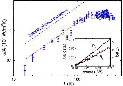
Next, we discuss the thermal conductance per unit cross section /A as a function of temperature. At room temperature /A is 3.8108 W/m2K (Figure 3). This value is comparable to the values observed in suspended exfoliated SLG samples based on Raman measurements (3-5108 W/m2K) balandin2 ; balandin3 . The high quality of CVD graphene is further confirmed by the temperature dependence of /A. It decreases by a factor of 100 to approximately 4.5106 W/m2K at 15 K. Such a steep decrease has not been observed previously, but more interestingly, the data at low temperatures can be fitted with 1.71051.53 W/m2K. This is shown as the dashed red curve in Figure 3 and has important implications for the nature of phonon transport. Mingo and Brodio proposed that for ballistic phonon transport, /A follows 61051.5 W/m2K ballisticMingo , as shown by the blue dashed curve in the same figure. The experimentally observed value is close to 30 of the predicted ballistic thermal conductance for graphene. From this we conclude that in our sample with a channel length of 500nm phonon transport approaches the ballistic limit. It is important to note that even in multiwalled CNT, the experimentally observed /A reached at most 40 of the ballistic limit in graphite Nanotube ; ballisticMingo . Deviation from ballistic transport in our experiment is most likely caused by scattering from PMMA residues, CVD graphene specific organic contamination, ripples and CVD graphene specific defects defectINCVD such as wrinkles. However, even in the absence of defects and contamination, two additional source remain: a) scattering from naturally existing 1.1 13C isotopic impurities isotopic and b) scattering from the boundaries between the suspended area and the supported areas on top of the contacts.
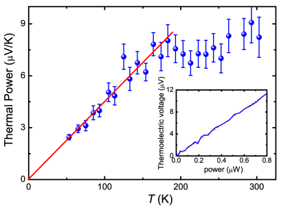
Last but not least, we discuss the thermoelectric power (TEP) of suspended graphene samples. Shown in the inset of Figure 4 is the linear thermoelectric voltage as a function of Joule heat in Rh (blue curve). Since TEP and its temperature dependence vary sharply across the Dirac point and we do not have a gate control, a direct comparison with supported samples is difficult. At room temperature the observed value is 9 V/K, suggesting a hole-like majority carrier. The linear fit (red curve in Figure 4) to our data can be extrapolated to zero at 0K. Similar to TEP measurements in supported graphene thermopower , this confirms the absence of phonon drag in suspended CVD SLG.
In conclusion we have measured phonon transport in suspended graphene as a function of temperature from 380 K down to 15K. We have taken advantage of the recent progress in Cu based CVD graphene and observed a power in these samples. Our results clearly show that the thermal conductance is strongly dominated by ZA phonons. At low temperatures phonon transport is approaching the ballistic limit, demonstrating the high quality of CVD graphene samples also in the context of heat transport.
Acknowledgements.
We thank Y. Zheng for helping with measurements and C.T. Toh for helping with fabrication. This work is supported in part by Singapore National Research Foundation (NRF-RF2008-07), NRF-CRP grant (R-143-000-360-281), by a NUS grant (R-144-000-222-646), by A*STAR grant (R-143-000-360-311), and by NUS NanoCore.References
- (1) A. Dhar, Adv. Phys. 57, 457 (2008); L. Wang and B. Li, Phys. World 21, 27 (2008).
- (2) K.S. Novoselov ., Science 306, 666 (2004); K.S. Novoselov ., Nature 438, 197 (2005); Y.B. Zhang, Y.W. Tan, H.L. Stormer and P. Kim, Nature 438, 201 (2005).
- (3) A.H. Castro Neto ., Rev. Mod. Phys. 81, 109 (2009).
- (4) E. Pop, Nano Res. 3, 147 (2010).
- (5) A.A. Balandin ., Nano Lett. 8, 902 (2008).
- (6) S. Ghosh ., Appl. Phys. Lett. 92, 151911 (2008).
- (7) S. Ghosh ., Nat. Mater. 9, 555 (2010).
- (8) L. Wei ., Phys. Rev. Lett. 70, 3764 (1993).
- (9) P. Kim, L. Shi, A. Majumdar and P.L. McEuen, Phys. Rev. Lett. 87, 215502 (2001).
- (10) E. Pop ., Nano Lett. 6, 96 (2006).
- (11) C. Faugeras ., Acs Nano 4, 1889 (2010).
- (12) W.W. Cai ., Nano Lett. 10, 1645 (2010).
- (13) J.H. Seol ., Science 328, 213 (2010).
- (14) X.S. Li ., Science 324, 1312 (2009).
- (15) S. Bae ., Nat. Nanotechnol. 5, 574 (2010).
- (16) N. Mingo and D.A. Broido, Phys. Rev. Lett. 95, 096105 (2005).
- (17) E. Muñoz, J.X. Lu and B.I. Yakobson, Nano Lett. 10, 1652 (2010).
- (18) C.W. Chang, D. Okawa, A. Majumdar and A. Zettl, Science 314, 1121 (2006).
- (19) R.K. Chen ., Phys. Rev. Lett. 101, 105501 (2008); A.I. Hochbaum ., Nature 451, 163 (2008).
- (20) L. Shi ., J. Heat Transfer 125, 881 (2003).
- (21) The grain size of CVD SLGs is in the order of 20m20m, while the devices for the thermal measurements have lateral dimensions of 3m1m. Hence, the samples have, if at all only one grain boundary at most.
- (22) please refer to the supplementary informaion for details.
- (23) X. Du, I. Skachko, A. Barker and E.Y. Andrei, Nat. Nanotechnol. 3, 491 (2008).
- (24) D.L. Nika, E.P. Pokatilov, A.S. Askerov and A.A. Balandin, Phys. Rev. B 79, 155413 (2009).
- (25) L. Lindsay, D.A. Broido and N. Mingo, Phys. Rev. B 82, 115427 (2010).
- (26) P.G. Klemens, Int. J. Thermophys., 22, 265 (2001).
- (27) W.Y. Jang ., Nano Lett. 10, 3909 (2010).
- (28) O.V. Yazyev and S.G. Louie, Nat. Mater. 9, 806 (2010).
- (29) J.W. Jiang, J.H. Lan, J.S. Wang and B. Li, J. Appl. Phys. 107, 054314 (2010).
- (30) Y.M. Zuev, W. Chang and P. Kim, Phys. Rev. Lett. 102, 096807 (2009); J.G. Checkelsky and N.P. Ong, Phys. Rev. B 80, 081413(R) (2009).