Coherent Heteroepitaxy of Bi2Se3 on GaAs (111)B
Abstract
We report the heteroepitaxy of single crystal thin films of Bi2Se3 on the (111)B surface of GaAs by molecular beam epitaxy. We find that Bi2Se3 grows highly c-axis oriented, with an atomically sharp interface with the GaAs substrate. By optimizing the growth of a very thin GaAs buffer layer before growing the Bi2Se3, we demonstrate the growth of thin films with atomically flat terraces over hundreds of nanometers. Initial time-resolved Kerr rotation measurements herald opportunities for probing coherent spin dynamics at the interface between a candidate topological insulator and a large class of GaAs-based heterostructures.
The narrow band gap semiconductor Bi2Se3 has recently emerged as a promising basis for creating a state of matter known as a topological insulator (TI) wherein protected states can be produced at the surface of the material via the locking of spin and momentum by the constraints of time reversal symmetry.Fu, Kane, and Mele (2007); Qi, Hughes, and Zhang (2008); Zhang et al. (2009a) The prediction that it has the requisite electronic structure for forming these special conducting surface states spanning its bulk electronic energy gap has been confirmed by angle resolved photoemission spectroscopy.Zhang et al. (2009a); Xia et al. (2009); Hsieh et al. (2009) With a bulk band gap ( 0.3 eV) larger than other relevant materials, Bi2Se3 is one of the best candidate materials for engineering of the Fermi energy into the bulk band gap so that transport can occur only through these surface states. However, this simple prescription has proved hard to realize because of an inherent tendency of the material to form Se vacancies or antisites that serve as donors,Navrátil et al. (2004) moving the Fermi energy far above the gap and making the contribution of the surface states to transport properties difficult to detect.Hor et al. (2009)
The growth of Bi2Se3 by molecular beam epitaxy (MBE) provides a potentially attractive solution for minimizing such defects by allowing for flexible control of growth conditions. To date, MBE growth of Bi2Se3 has been demonstrated on several substrates, including silicon, graphene and SrTiO3, albeit without complete removal of midgap states.Zhang et al. (2009b); Li et al. (2010); Zhang et al. (2010); Song et al. (2010); Chen et al. (2010) For silicon, the MBE growth of single crystal Bi2Se3 requires the introduction of an intermediate layer (e.g. a monolayer of Bi or amorphous layers) that improves the film quality by effectively decoupling it from the substrate, while graphene is conductive, complicating transport measurements of the surface states. In this Letter, we report the heteroepitaxy of Bi2Se3 thin films upon another technologically important substrate material, GaAs. Notably, we show that the epitaxial growth is coherent with the substrate, thus opening routes for exploring the coupling of spin polarized TI states with electronic states in a wide variety of advanced semiconductor heterostructures, including magnetically doped III-V and II-VI semiconductors.
We carried out MBE growth of Bi2Se3 thin films on epiready, semi-insulating GaAs (111)B substrates using thermal evaporation of high purity (5N) elemental Bi and Se from conventional Knudsen cells. After thermal desorption of the native oxide on the substrate under an arsenic flux, we first deposited a very thin GaAs buffer layer (18 monolayers), yielding a very flat GaAs surface without the pitting of the surface that occurs with desorption of the oxide or the three dimensional hillocks that form with thicker buffers.Sugahara and Tanaka (2003) Bi2Se3 was then grown at a substrate thermocouple temperature of 400 ∘C (corresponding to an estimated actual substrate temperature of C) and a Se:Bi beam equivalent pressure ratio ranging from 10:1 to 30:1.
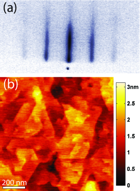
Bi2Se3 has a tetradymite, trigonal crystal structure with a rhombohedral unit cell that can be viewed as consisting of three sets of groupings of Se-Bi-Se-Bi-Se planes commonly referred to as quintuple layers (QLs). Each Se or Bi plane within the QL is a two dimensional hexagonal lattice. This matches the hexagon structure of the GaAs (111) surface with a lattice mismatch of 3.55%. We have grown Bi2Se3 films ranging in thickness from nm down to a few QLs ( nm) with a typical growth rate of 0.85 QL/min. Reflection high energy electron diffraction (RHEED) measurements during growth of Bi2Se3 indicate an unreconstructed surface (Fig. 1(a)). We have also observed RHEED oscillations of the specular spot (data not shown), with each oscillation corresponding to the growth of a QL, indicating that the Bi2Se3 thin films grow layer-by-layer.Song et al. (2010); Li et al. (2010)
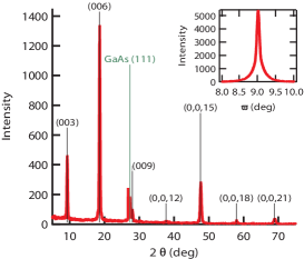
The morphology of the films was studied ex-situ by atomic force microscopy (AFM). For some films, like the 25 nm thick film shown in Fig. 1(b), we grew a second buffer of ZnSe, only a few monolayers thick, by atomic layer epitaxy. While we were unable to directly confirm the presence of ZnSe in these samples by x-ray diffraction (XRD) or Raman spectroscopy, they did tend to result in very flat Bi2Se3 surfaces with RMS roughnesses of nm. Samples without the ZnSe buffer were slightly rougher with an average RMS roughness of a few nm. Very thin films of 2-3 QLs appear to exhibit island-like growth, similar to observations made for growth of Bi2Se3 on graphene.Song et al. (2010) XRD measurements show reflections only from the (003) family of planes of the film, indicating that the films are highly c-axis oriented along the growth direction (Fig. 2). The rocking curve yielded a full width half maximum of 0.1∘, significantly better than those reported for growth on vicinal Si substrates with an amorphous layer.Li et al. (2010). While including a ZnSe buffer resulted in a flatter film, it also resulted in a wider rocking curve.
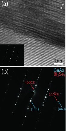
To confirm the epitaxial growth of the Bi2Se3 thin film, we have carried out high-resolution transmission electron microscopy (HRTEM) on one of the samples grown directly on the thin GaAs buffer. Fig. 3(a) shows a typical HRTEM image at the interface of Bi2Se3 and GaAs. The lattice fringes of the phase contrast images show a good registry between the film and substrate without any amorphous growth or secondary phases occurring at the interface. The inset shows a selected area diffraction (SAD) pattern from just the GaAs substrate. Fig. 3(b) shows the SAD pattern from the whole region spanning the interface. Besides the pattern due to GaAs (blue indexes), the new spots (red indexes) are consistent with a single crystal Bi2Se3 film that has grown epitaxially on the GaAs. The interplanar distance between Bi2Se3 (220) and GaAs (440) is found to be 0.336 nm-1 in reciprocal space yielding a lattice mismatch in the plane of 3.62%, consistent with the expected value of 3.55%, and indicating that the film is relaxed. Surprisingly, we do not find any evidence of twinning or dislocations in the TEM study, despite the large lattice mismatch. Both the HRTEM images and the diffraction patterns from several different areas show that the Bi2Se3 thin films are generally high-quality single crystals with a low density of defects.
Electrical transport studies were carried out at 4.2 K using lithographically patterned and wet etched Hall bars (with dimensions of 650 m 400 m) in perpendicular magnetic fields up to 4 T. Electrical and Hall conductivity measurements reveal that all the samples studied are n-doped with carrier densities in the range cm cm-3 and mobilities in the range cm2 (V.s)-1, consistent with previous reports of MBE growth.Li et al. (2010) Thus, we are still faced with unintentional background doping, presumably from a lack of stoichiometry and perhaps some contributions from unintentional Cd contamination from an earlier source in our MBE chamber. Magnetoresistance (MR) curves are shown in Fig. 4(a) for various film thicknesses. All show a positive MR cusp, consistent with weak anti-localization corrections to diffusive transport and typical of measurements of Bi2Se3 reported in the literature.Checkelsky et al. (2009); Peng et al. (2010) A systematic analysis of the temperature, magnetic field and sample thickness dependence of the MR will be reported elsewhere.
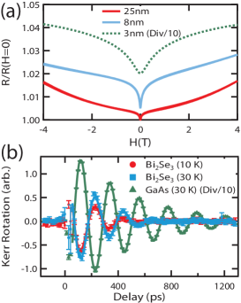
Finally, we discuss preliminary magneto-optical measurements that probe spin-dependent phenomena associated with the interface in these heterostructures. We used a well-established time-resolved Kerr rotation (TRKR) technique Kikkawa and Awschalom (1998) to demonstrate a possible method of probing spin polarization in a TI via coupling to spin states in a conventional semiconductor. Figure 4(b) shows TRKR curves for optically-injected spins in the GaAs substrate precessing in an in-plane magnetic field. Data measured through an 8 nm layer of Bi2Se3 are shown at two temperatures, along with reference data from an area where the Bi2Se3 layer was wet-etched away. By fitting the TRKR to a damped sinusoid,Kikkawa and Awschalom (1998) we deduce the g-factor and the inhomogeneous spin lifetime (). While the g-factor of spins in GaAs () is unchanged by overgrowth of Bi2Se3, is significantly shorter at the Bi2Se3 interface: at K, ps at the interface, compared with ps in the reference region.
In summary, we have demonstrated the coherent epitaxial growth of the candidate TI material Bi2Se3 on GaAs (111)B substrates. The ability to synthesize Bi2Se3 epitaxial films with high quality heterointerfaces on GaAs and ZnSe opens the door to a host of interesting heterostructure applications, including TI-magnetic semiconductor interfaces, where magnetic monopoles or Majorana fermions at domain walls could be studied.Qi et al. (2009); Akhmerov, Nilsson, and Beenakker (2009)
We thank Josh Maier for preparing the cross-sectional TEM specimen. This work was supported by the Penn State MRSEC (NSF-DMR-0820404) through a seed grant and the REU program, and partially by grants ONR N00014-09-1-0221 and -0309. We acknowledge use of the NSF National Nanofabrication Users Network Facilities at Penn State and UCSB.
References
- Fu, Kane, and Mele (2007) L. Fu, C. L. Kane, and E. J. Mele, Phys. Rev. Lett. 98, 106803 (2007).
- Qi, Hughes, and Zhang (2008) X.-L. Qi, T. L. Hughes, and S.-C. Zhang, Phys. Rev. B 78, 195424 (2008).
- Zhang et al. (2009a) H. Zhang, C.-X. Liu, X.-L. Qi, X. Dai, Z. Fang, and S.-C. Zhang, Nat. Phys. 5, 438 (2009a).
- Xia et al. (2009) Y. Xia, D. Qian, D. Hsieh, L. Wray, A. Pal, H. Lin, A. Bansil, D. Grauer, Y. S. Hor, R. J. Cava, and M. Z. Hasan, Nat. Phys. 5, 398 (2009).
- Hsieh et al. (2009) D. Hsieh, Y. Xia, D. Qian, L. Wray, J. H. Dil, F. Meier, J. Osterwalder, L. Patthey, J. G. Checkelsky, N. P. Ong, A. V. Fedorov, H. Lin, A. Bansil, D. Grauer, Y. S. Hor, R. J. Cava, and M. Z. Hasan, Nature 460, 1101 (2009).
- Navrátil et al. (2004) J. Navrátil, J. Horák, T. Plechacek, S. Kamba, P. Lostak, J. Dyck, W. Chen, and C. Uher, J. Solid State Chem. 177, 1704 (2004).
- Hor et al. (2009) Y. S. Hor, A. Richardella, P. Roushan, Y. Xia, J. G. Checkelsky, A. Yazdani, M. Z. Hasan, N. P. Ong, and R. J. Cava, Phys. Rev. B 79, 195208 (2009).
- Zhang et al. (2009b) G. Zhang, H. Qin, J. Teng, J. Guo, Q. Guo, X. Dai, Z. Fang, and K. Wu, Appl. Phys. Lett. 95, 053114 (2009b).
- Li et al. (2010) H. D. Li, Z. Y. Wang, X. Kan, X. Guo, H. T. He, Z. Wang, J. N. Wang, T. L. Wong, N. Wang, and M. H. Xie, ArXiv e-prints (2010), 1005.0449 .
- Zhang et al. (2010) Y. Zhang, K. He, C.-Z. Chang, C.-L. Song, L.-L. Wang, X. Chen, J.-F. Jia, Z. Fang, X. Dai, W.-Y. Shan, S.-Q. Shen, Q. Niu, X.-L. Qi, S.-C. Zhang, X.-C. Ma, and Q.-K. Xue, Nat. Phys. 6, 584 (2010).
- Song et al. (2010) C.-L. Song, Y.-L. Wang, Y.-P. Jiang, Y. Zhang, C.-Z. Chang, L. Wang, K. He, X. Chen, J.-F. Jia, Y. Wang, Z. Fang, X. Dai, X.-C. Xie, X.-L. Qi, S.-C. Zhang, Q.-K. Xue, and X. Ma, Appl. Phys. Lett. 97, 143118 (2010).
- Chen et al. (2010) J. Chen, H. J. Qin, F. Yang, J. Liu, T. Guan, F. M. Qu, G. H. Zhang, J. R. Shi, X. C. Xie, C. L. Yang, K. H. Wu, Y. Q. Li, and L. Lu, Phys. Rev. Lett. 105, 176602 (2010).
- Sugahara and Tanaka (2003) S. Sugahara and M. Tanaka, J. Cryst. Growth 251, 317 (2003).
- Checkelsky et al. (2009) J. G. Checkelsky, Y. S. Hor, M.-H. Liu, D.-X. Qu, R. J. Cava, and N. P. Ong, Phys. Rev. Lett. 103, 246601 (2009).
- Peng et al. (2010) H. Peng, K. Lai, D. Kong, S. Meister, Y. Chen, X.-L. Qi, S.-C. Zhang, Z.-X. Shen, and Y. Cui, Nat Mater 9, 225 (2010).
- Kikkawa and Awschalom (1998) J. M. Kikkawa and D. D. Awschalom, Phys. Rev. Lett. 80, 4313 (1998).
- Qi et al. (2009) X.-L. Qi, R. Li, J. Zang, and S.-C. Zhang, Science 323, 1184 (2009).
- Akhmerov, Nilsson, and Beenakker (2009) A. R. Akhmerov, J. Nilsson, and C. W. J. Beenakker, Phys. Rev. Lett. 102, 216404 (2009).