Measurement of valley splitting in high-symmetry Si/SiGe quantum dots
Abstract
We have demonstrated few-electron quantum dots in Si/SiGe and InGaAs, with occupation number controllable from . These display a high degree of spatial symmetry and identifiable shell structure. Magnetospectroscopy measurements show that two Si-based devices possess a singlet ground state at low magnetic field, and therefore, the two-fold valley degeneracy is lifted. The valley splittings in these two devices were and , suggesting the presence of atomically sharp interfaces in our heterostructures.
Quantum dots fabricated in silicon have been a subject of intense interest recently due to the possibility of their use for semiconductor-based quantum information processing.Eriksson An important requirement in silicon is the ability to lift the conduction band valley degeneracy,Eriksson which is commonly two-fold in the strained Si heterostructure. A lower bound on the valley splitting in a Si quantum dot can be determined by ground state magnetospectroscopy on the first few electron states.Hada Recently, this technique has been applied to metal-oxide-semiconductor-based quantum dotsXiao ; Lim ; Lim2 and a range of values has been obtained. However, no valley splitting measurements in Si/SiGe quantum dots have been reported, only estimates from transport data in quantum point contacts (QPC).Goswami ; *McGuire In the Si/SiGe system, electrons are confined against a buried heterointerface as opposed to the interface. This isolates the electrons from surface traps, but leads to potentially different valley physics. In this Letter we report electron addition spectra for accumulation mode Si/SiGe quantum dots, starting from the first electron. Spectra for equivalent devices fabricated in InGaAs provides validation of our numerical simulations and the high axial symmetry provided by this design. We additionally report measured spin fillings via magnetospectroscopy for two Si/SiGe dots in which clear changes in total spin with magnetic field allow us to extract valley splittings up to .
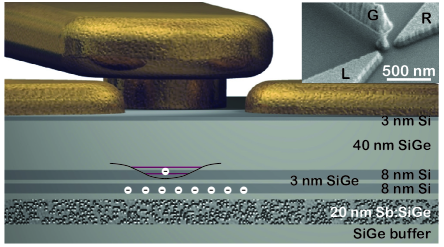
The device design is based on a gated double quantum well heterostructure as shown in Fig. 1. This design has been realized in both InGaAs, as previously reported by our group,Croke and now in Si/SiGe. The Si/SiGe heterostructures were grown on strain-relaxed buffers () and formed two-dimensional electron gases supporting mobilities greater than at carrier concentrations. A quantum dot is created in a potential depression in the upper quantum well under the influence of a nominally diameter circular forward biased gate that is contacted via an air-bridged (dielectric-bridged for device Si4) lead. A pair of reverse-biased gates form a QPC in the lower quantum well electron gas, within of the quantum dot, for charge detection.

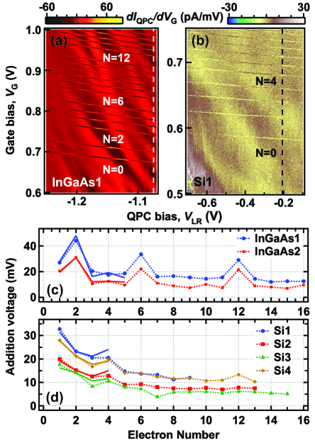
Six individual devices, having slight variations in dot gate diameter and dot-QPC distance, were selected from four Si/SiGe and two InGaAs wafers and measured in either a 3He system at an effective electron temperature of or a dilution refrigerator at (device Si4 only). Addition spectra were taken using lock-in techniques similar to that described in Croke et al.Croke Loading of electrons into the dot was recorded by sweeping the quantum dot gate bias and recording the resulting change in conductance on the constricted current flowing through the nearby QPC. The dc source-drain bias was kept to a modest across the QPC, as larger currents flowing through the charge sensor were found to broaden the dot transitions. A differential transconductance was extracted by measuring the in-phase response of the QPC current to small sinusoidal or square wave modulation of (at modulation frequencies well below the tunneling rates for each respective device). The modulation amplitude was kept as large as possible without broadening the transitions (typically 0.2 mV). Figures 2(a) and 2(b) show representative high resolution scans of in space of gate and QPC biases, obtained for the InGaAs (left) and Si/SiGe (right) accumulation mode devices.

The identification of the last transition as , in terms of the absolute occupation number , was established by observing that the tunneling times between the dot and electron reservoir (lower quantum well), , show no significant variation with electron number, as found by analysis of the time-averaged charge dynamics for the first few observable transitions. Furthermore, our numerical simulations predict the observed addition spectra including in particular first electron filling voltages and spin fillings.
In Figs. 2(c) and 2(d) the addition voltages are plotted for all six measured dots. These data are taken at values of the QPC biases that provided the largest sustained sensitivity that captured all of the observed electron loading transitions [in particular, along dashed vertical lines in Figs. 2(a) and 2(b)]. Addition energies can be obtained from these addition voltages via an independent measure of the gate lever arm , in which the linewidth of the transitions is monitored as a function of sample temperature.Meirav For the series of devices under study is measured to be (InGaAs1), (InGaAs2), (Si1), (Si2), (Si3), within of our numerically simulated values. The simulated value for Si4 is .
The solid curves in Figs. 2(c) and 2(d) are simulated addition voltages computed in the framework of the full configuration interaction (FCI) method.Szabo They are found as the difference of chemical potentials, , for electron addition and converted to voltage differences via concurrently simulated values of : . The chemical potentials, , are computed as the differences between ground state energies of the and electron systems. Two valleys are explicitly accounted for in the case of Si/SiGe. Accurate simulations using the computationally intensive FCI technique are only available up to five (six) electrons for Si (InGaAs) resulting in the first four (five) addition energies.
First shell filling is observed at for all four Si dots, as evidenced by the larger addition energy relative to the monotonically decaying Coulomb background. This first shell is much less prominent in Si due to the smaller orbital energy by a factor of while having comparable charging energies to InGaAs. Si4 displays the most prominent shell, best matching simulation, as well as having a distinct shell at . This is likely due to improvements in our process leading to more symmetric metallization of the dot gates. The shell structure that we observe in InGaAs is the result of two-dimensional parabolic confinement and spin degeneracy,Tarucha ; Reimann whereas that for Si indicates an additional two-fold valley degeneracy as expected.

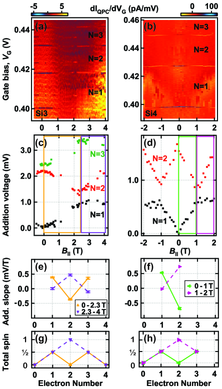
The sequences of spin fillings for these devices are obtained by performing magnetospectroscopy measurements. The application of an in-plane magnetic field, , modifies the energetics of the -electron system primarily through the Zeeman term in the Hamiltonian. Measuring the dots’ transitions as a function of both gate voltage and magnetic field allows inference of the total projected spin state of the dot as a function of electron number for various .Weis ; Potok ; Hanson In Figs. 3(a) and 3(b) we plot the differential transconductance for devices Si3 and Si4 versus gate bias and stepped magnetic field, collected in largely the same manner as for the addition spectra of Figs. 2(a) and 2(b). The centers of each transition versus are extracted from the data by fitting the surrounding 2 mV data to a Gaussian function with fixed linewidth. All fits with transition center uncertainties less than a fixed threshold are included in subsequent analysis. In order to remove spin-independent effects on the chemical potentials,Weis the separations between transitions are calculated and plotted in Figs. 3(c) and 3(d). Slopes from piecewise linear fits for magnetic fields in the four boxed regions of Figs. 3(c) and 3(d), are shown along with error bars in Figs. 3(e) and 3(f), consistent with multiples of the expected for . Taking and , the total spin state can be inferred from the addition slopes, Figs. 3(g) and 3(h).Weis ; Potok ; Hanson
The spin state of device Si3 demonstrates a singlet-triplet (S-T) transition at as evidenced by the change from the spin filling sequence at low fields to at higher fields. Device Si4 demonstrates an identical S-T transition at a lower magnetic field . For devices Si1 and Si2 only a triplet state was observed down to zero magnetic field.Si1Si2 Device InGaAs2 displayed the expected Hund’s rule spin filling out to the third shell.InGaAs2 ; Tarucha
The magnetic field corresponding to the S-T transition indicates the energy of the lowest lying triplet state; from we find and for device Si3 and Si4, respectively. As the intervalley exchange energy is negligible, this is a strict lower bound on the valley splitting, .Hada The equality likely holds due to the large orbital energies of these high-symmetry quantum dots. Further validation is provided by our calculations of the valley splitting in a microscopically-based framework which directly incorporates into the effective mass calculation the core physical origin of intervalley mixing — the change to the local crystal potential due to substitution of individual host atoms in a heterostructure. A value is predicted for the ground orbital in both Si3 and Si4 devices for the case of perfectly flat and atomically sharp heterointerfaces; the splitting would be reduced in the presence of interface imperfections.
We have demonstrated high-symmetry quantum dots in Si/SiGe and InGaAs, with occupation number controllable from . Magnetospectroscopy measurements reveal a valley non-degenerate ground state for two Si dots, a critical requirement for the eventual control and manipulation of single spins in this system.Eriksson ; Hanson
The authors gratefully acknowledge Thaddeus Ladd and Professor Charles Marcus for many useful discussions. Sponsored by United States Department of Defense. The views and conclusions contained in this document are those of the authors and should not be interpreted as representing the official policies, either expressly or implied, of the United States Department of Defense or the U.S. Government. Approved for public release, distribution unlimited.
References
- (1) M. A. Eriksson, M. Friesen, S. N. Coppersmith, R. Joynt, L. J. Klein, K. Slinker, C. Tahan, P. M. Mooney, J. O. Chu, and S. J. Koester, Quantum Information Processing, 3, 133 (2004).
- (2) Y. Hada and M. Eto, Phys. Rev. B, 68, 155322 (2003).
- (3) M. Xiao, M. G. House, and H. W. Jiang, Appl. Phys. Lett., 97, 032103 (2010).
- (4) W. H. Lim, F. A. Zwanenburg, H. Huebl, M. Möttönen, K. W. Chan, A. Morello and A. S. Dzurak, Appl. Phys. Lett. 95, 242102 (2009).
- (5) W. H. Lim arXiv:1103.2895 (unpublished).
- (6) S. Goswami, K. A. Slinker, M. Friesen, L. M. McGuire, J. L. Truitt, C. Tahan, L. J. Klein, J. O. Chu, P. M. Mooney, D. W. Van der Weide, R. Joynt, S. N. Coppersmith, and M. A. Eriksson, Nat. Phys. 3, 41 (2007).
- (7) L. M. McGuire, M. Friesen, K. A. Slinker, S. N. Coppersmith and M. A. Eriksson, New J. Phys., 12, 033039 (2010).
- (8) E. T. Croke, M. G. Borselli, M. F. Gyure, S. S. Bui, I. I. Milosavljevic, R. S. Ross, A. E. Schmitz, and A. T. Hunter, Appl. Phys. Lett. 96, 042101 (2010).
- (9) U. Meirav and E. B. Foxman, Semicond. Sci. Tech. 11, 255, (1996).
- (10) A. Szabo and N. S. Ostlund, Modern Quantum Chemistry (Dover, New York, 1996).
- (11) S. Tarucha, D. G. Austing, T. Honda, R.J. van der Hage, and L. P. Kouwenhoven, Phys. Rev. Lett. 77, 3613 (1996).
- (12) S. M. Reimann and M. Manninen, Rev. Mod. Phys. 74 1283 (2002).
- (13) J. Weis, R. J. Haug, K. V. Klitzing, and K. Ploog, Phys. Rev. Lett. 71, 4019 (1993).
- (14) R. M. Potok, J. A. Folk, C. M. Marcus, V. Umansky, M. Hanson, A. C. Gossard, Phys. Rev. Lett. 91, 016802 (2003).
- (15) R. Hanson, L. P. Kouwenhoven, J. R. Petta, S. Tarucha, L. M. K. Vandersypen, Rev. of Mod. Phys. 79, 1217 (2007).
- (16) Magnetospectroscopy on devices Si1 and Si2 display first addition slopes of and , respectively, from to T.
- (17) Magnetospectroscopy on device InGaAs2 displays three complete shells and nine non-zero addition slopes with an average and standard deviation . With , this results in a .