Energy-efficient mixed mode switching of a multiferroic nanomagnet for logic and memory
Abstract
In magnetic memory and logic devices, a magnet’s magnetization is usually flipped with a spin polarized current delivering a spin transfer torque (STT). This mode of switching consumes too much energy and considerable energy saving can accrue from using a multiferroic nanomagnet switched with a combination of STT and mechanical stress generated with a voltage (VGS). The VGS mode consumes less energy than STT, but cannot rotate magnetization by more than 90∘, so that a combination of the two modes is needed for energy-efficient switching.
In magnetic logic and memory devices, the magnetization of a nanomagnet is usually switched with a spin-polarized current delivering a spin transfer torque RefWorks:7 ; RefWorks:124 . This is a well-established technique that has been experimentally demonstrated in different systems RefWorks:43 ; RefWorks:32 and is widely used for spin transfer torque random access memory (STTRAM).
Unfortunately, this method of switching dissipates too much energy and a more energy-saving approach is to rotate the magnetization of a multiferroic nanomagnet – consisting of a piezoelectric layer and a magnetostrictive layer – with an electrostatic potential applied to the piezoelectric layer RefWorks:154 . The applied voltage generates stress in the magnetostrictive layer, which rotates its magnetization. Such rotations have been experimentally demonstrated RefWorks:167 . Recently, we showed that this can implement Bennett clocking in nanomagnetic logic arrays RefWorks:154 where a very small voltage of 16 mV can rotate the magnetization of a shape-anisotropic multiferroic nanomagnet (made of lead zirconium titanate (PZT) and Terfernol-D) by 90∘ to carry out Bennett clocking. The energy dissipated is only 60 at room temperature and the rotation takes about 80 ns to complete fasha10 . The time can be reduced to 3 ns by increasing the stress to the maximum that PZT might be able to generate in the Terfenol-D layer, but that also increases the energy dissipation to about 48,000 fasha10 . Still, this is considerably smaller than the energy that would have been expended had we clocked the same nanomagnet with spin transfer torque (STT) in the same 3 ns fasha10 .
Unfortunately, the voltage-generated-stress (VGS) mode of switching has a major shortcoming. It can rotate an isolated magnet’s magnetization by nearly 90∘ (e.g. from the easy to the hard axis of a shape anisotropic magnet) but cannot rotate past 90∘ to achieve a complete flip. Thus, it may be adequate for Bennett clocking which requires rotation by 90∘, but inadequate for writing a bit in STTRAM, which requires 180∘ rotation. Therefore, we have devised a mixed-mode approach where both VGS and STT are employed to rotate a magnet’s magnetization by 180∘. We will show that this mixed mode switching (MMS) results in considerable energy saving at any given switching delay compared to using just the STT mode.

In order to study the MMS paradigm, we have solved the appropriate Landau-Lifshitz-Gilbert (LLG) equation analytically. Our nanomagnet is an elliptical multiferroic consisting of a 2 nm/3.5 nm thick layer of Terfenol-D/nickel (magnetostrictive) and a 40 nm thick layer of PZT (piezoelectric) as shown in Fig. 1. Its major and minor axes are 220 nm and 100 nm, respectively, which we tacitly assume precludes formation of multiple domains. This shape anisotropy causes an energy barrier of 32 to appear between the two minimum energy states along the major axis (easy axis). We assume that the magnet’s plane is the y-z plane and the easy axis is along the z-axis. The angle subtended by the nanomagnet with the +z-axis is denoted as (see Fig. 1).
Solution of the LLG equation yields the time rate of change of the angle . The derivation can be found in the supplementary material, but the final expression is
| (1) |
where is the Gilbert damping constant of the magnetostrictive layer, is the volume of that layer, is the gyromagnetic ratio, (energy barrier due to shape anisotropy), is the saturation magnetization of the magnetic layer, is the permeability of free space, and are the demagnetization factors in the y- and z-directions, respectively, (stress-anisotropy energy), is the magnetostrictive coefficient of the polycrystalline magnetic layer, is the stress, , , is the in-plane spin polarized current inducing STT, is the spin polarization of the current, and is the angle between the spin polarization of the current and the +z-axis. In an actual STTRAM configuration, where there will be two magnets separated by an insulating layer, the quantity will be replaced by the quantity , where and are dimensionless voltage-dependent quantities RefWorks:92 , but for an isolated magnet, they do not arise.
In order to flip the magnetization from –z to the +z direction, the spins in the spin polarized current must be aligned along the +z-direction so that .
From Equation (1), we can obtain the time required to rotate the magnetization from an initial orientation to a final orientation as
| (2) |
We will assume that the initial orientation is aligned close to the –z-axis so that . If and the magnetization is exactly along the easy axis, then no amount of stress or spin polarized current can budge it since the effective torque exerted on the magnetization by either stress or spin polarized current will be exactly zero. Such locations are called “stagnation points”. Therefore, we will assume that . This is not an unreasonable assumption since thermal fluctuations can dislodge the magnetization from the easy axis and make .
We now consider three different scenarios: pure stress mediated switching (VGS), pure spin transfer torque mediated switching (STT) and mixed mode switching (MMS).
In the pure VGS switching mode, the time taken to rotate the magnetization from the initial orientation to () is obtained from Equation (2) as
| (3) | |||||
The above equation shows that stress will take infinite time to complete the rotation if either , or . Thus, initial alignment along the easy axis or final alignment along the hard axis is forbidden. The physics behind the stagnation points can be understood by looking at the energy profile of the nanomagnet as a function of (see the supplementary material for an expression that relates to ). Without spin transfer torque, the energy consists of only the shape anisotropy energy and the stress anisotropy energy. The slope of this energy profile at and 180∘ is exactly zero, which means that there is no torque acting on the nanomagnet at these orientations to cause any rotation. This ensures that the pure VGS mode can never rotate the magnetization past 90∘. It can rotate the magnetization from close to the easy axis to close to the hard axis, which is adequate for Bennett clocking of nanomagnetic logic RefWorks:154 , but not adequate for writing bits in MRAM.
Next, let us consider the pure STT switching mode with no stress present. The time required to rotate the magnetization from an initial orientation to a final orientation is obtained from Equation (2) as (see supplementary material)
| (4) |
where and is an arbitrary angle. The above expression is invalid for since then the energy imparted by the spin transfer torque will not be sufficient to overcome the energy barrier due to shape anisotropy and cause rotation of the magnetization.
The last expression shows that the time to complete the rotation approaches infinity if , indicating that spin transfer torque has a stagnation point at and , i.e. when the final or the initial state of the nanomagnet is along the easy axis. However, there is no stagnation point at the hard axis (), unlike in the case of VGS. Hence, thermal fluctuations are needed to nudge the magnetization slightly away from the easy axis so that spin transfer torque can nearly complete the flip. Once again, the origin of the stagnation points can be understood by noting that no spin transfer torque acts on the nanomagnet at these locations.
If thermal fluctuations deflect the nanomagnet from the easy axis by an angle , then the time needed to complete a near-flip is obtained from Equation (4) by setting . Note that becomes exponentially longer as approaches zero, so that one can nearly, but not completely, flip magnetization with STT.
For the MMS mode, we consider the following switching sequence which results in the most energy saving. Stress is applied abruptly to initiate the switching and rotate the magnetization from its initial orientation along to (), then a constant spin polarized current is turned on instantaneously. Thereafter, the sign of the stress is reversed abruptly as soon as the hard axis is crossed, and then the spin polarized current is turned off instantaneously when . Finally stress is removed when . This completes the switching by rotating the nanomagnet from to , where in our simulations. From Equation (2), the time required to rotate from to is , where and are given by
| (5) |
where . The upper sign denotes the switching delay for the rotation from to and the lower sign denotes the switching delay for the rotation from to . We add to this the time to rotate with stress alone between to and from to which are obtained from Equation (3).
Our next task is to compute the energy dissipations in the different switching modes. Since the pure VGS mode cannot rotate past the hard axis and flip the magnetization, we shall not consider it further and concentrate instead on the pure STT mode and the MMS mode.
In the pure STT mode, we will first pick a switching delay and then back out the current needed to switch in that time from Equation (4) using appropriate material values for nickel and Terfenol-D given in the supplementary material. The energy dissipated is then computed as , where is the resistance of the magnetostrictive layer. This allows us to plot versus for the pure STT mode.
In the MMS mode, the energy dissipated is , where is the capacitance of the piezoelectric layer (estimated as 3.8 fF for the dimensions of the multiferroic nanomagnet and assuming a relative dielectric constant of 1000 for the PZT), is the voltage applied on the multiferroic to generate a given stress , and is the spin polarized current needed to rotate the magnetization from to and complete the switching in time in the company of that given stress. We pick a stress and a , and then back out the current from Equation (5) that will be needed to complete the switching in time while applying STT in the angle interval [180∘ - , ]. Clearly, depends on . Therefore, we have to first find for given and as a function of (see supplementary material for a plot of versus ). We then choose that value of for which the is minimum since that will yield the most energy efficient switching scheme. For this optimum value of , we find and repeat this procedure for every , .
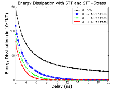
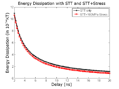
In Fig. 2, we plot the energy dissipations for the pure STT mode and the MMS mode as a function of delay in both Terfenol-D/PZT and nickel/PZT multiferroics with stress as a parameter. Typical switching delays of magnets contemplated for STTRAM is 2–20 ns srcm09 , which is why we plot within this range of delay. In this range, MMS is always superior to STT in the same material, and the energy saving increases with increasing delay since a larger portion of the rotation role can be handed over to stress if we allow for a larger delay. The saving is very pronounced in Terfenol-D/PZT (3 orders of magnitude at long delays) but much less pronounced for nickel (36% at long delays of 20 ns). However, for delays exceeding 6 ns, the MMS mode in Terfenol-D/PZT is more energy efficient than both the pure STT in nickel and the MMS mode in nickel/PZT.
In conclusion, we have shown MMS mode switching can be considerably more energy-efficient than STT mode. This could potentially lead to a new family of magnetic logic and memory devices based on multiferroics that are switched with a combination of voltage-generated stress and spin polarized current.
References
- (1) J. Z. Sun, Phys. Rev. B 62, 570 (2000).
- (2) B. Behin-Aein, et al., IEEE Trans. Nanotech. 8, 505 (2009).
- (3) J. A. Katine, et al., Phys. Rev. Lett. 84, 3149 (2000).
- (4) G. D. Fuchs, et al., Phys. Rev. Lett. 96, 186603 (2006).
- (5) J. Atulasimha et al., Appl. Phys. Lett. 97, 173105 (2010).
- (6) T. Brintlinger, et al., Nano. Lett. 10, 1219 (2010).
- (7) M. S. Fashami, et al., Nanotechnology (submitted) (2010).
- (8) D. Datta, et al., Arxiv preprint arXiv:0910.2489 (2009).
- (9) www.src.org/calendar/e003676/FinalReport.pdf (2009).