Evidence for electron-electron interaction in topological insulator thin films
Abstract
We consider in our work single crystal thin films of Bi2Se3, grown by molecular beam epitaxy, both with and without Pb doping. Angle-resolved photoemission data demonstrate topological surface states with a Fermi level lying inside the bulk band gap in the Pb doped films. Transport data show weak localization behavior, as expected for a thin film in the two-dimensional limit (when the thickness is smaller than the inelastic mean free path), but a detailed analysis within the standard theoretical framework of diffusive transport shows that the temperature and magnetic field dependences of resistance cannot be reconciled in a theory that neglects inter-electron interactions. We demonstrate that an excellent account of quantum corrections to conductivity is achieved when both disorder and interaction are taken into account. These results clearly demonstrate that it is crucial to include electron electron interaction for a comprehensive understanding of diffusive transport in topological insulators. While both the ordinary bulk and the topological surface states presumably participate in transport, our analysis does not allow a clear separation of the two contributions.
I Introduction
Topological structures in condensed matter often result from interactions; examples include vortices in superconductors, superfluids, two-dimensional XY systems, and the fractional quantum Hall effect. Topology also governs the behavior of certain non-interacting systems: the integer quantum Hall effect is the quintessential example, while the recently proposed topological band insulators provide another. The latter are predicted to contain conducting surface states with an odd number of Dirac cones that are topologically protected against time reversal invariant perturbation. Fu2007 ; Moore2007 ; Roy2009 ; Qi2008 It is important to demonstrate that the topological features of these new systems are robust to interparticle interaction. The existence of surface states has been investigated and confirmed for several candidate topological insulators using angle-resolved photoemission spectroscopy (ARPES). Hsieh2009 ; Hasan2010 Detecting these surface states by transport, which might at first appear the most natural probe, has proved more challenging, largely because of non-negligible bulk conduction. Here, we report a detailed study of the temperature and magnetic field dependence of the conductivity in topological insulator thin films grown by molecular beam epitaxy. A theoretical analysis of the observed quantum corrections to the conductivity unambiguously demonstrates that electron-electron interactions play a crucial role in determining the diffusive transport behavior of topological insulators.
Bi2Se3 is a candidate for a three dimensional topological insulator (TI), provided its Fermi level can be shifted to lie inside the bulk energy gap, as can be accomplished by appropriate amount of doping. Due to its relatively large band gap (0.3 eV) and its simple surface state structure (a single Dirac cone), it has become the canonical reference material for the 3D TIs. Zhang2009 ; Hasan2010 ; Qi2010 Several transport experiments have suggested the presence of conducting surface states in candidate 3D TIs. A large magnetofingerprint signalCheckelsky2009 in macroscopic crystals of nonmetallic Bi2Se3, Aharonov-Bohm oscillations in Bi2Se3 nanoribbonsPeng2010 with dimensions of 100 nm, and Shubnikov-de Haas (SdH) oscillationsQu2010 in bulk TI (Bi2Te3) have been reported and associated with the surface states. However, another SdH measurement on high quality Bi2Se3 single crystals did not find significant contributions from surface states and suggested that these are subject to strong scattering. Butch2010 It is noted that the analysis of all the above experiments neglects interactions.
Recent progress in thin film growth of TI materials by molecular beam epitaxy (MBE) Cheng2010 ; Zhang2010 has enabled the fabrication of thin films of crystalline Bi2Se3. We study the temperature and magnetic field dependence of two thin films of Bi2Se3, one undoped and the other doped. The latter is doped with an appropriate concentration of Pb, which should ideally render the bulk insulating. ARPES measurements demonstrate that the latter thin film possesses Dirac-cone surface states with the Fermi level lying in the bulk band gap. Although it is likely that there is bulk conduction in the doped thin film as well, the expectation is that the contribution from surface states will make a significant contribution to the electrical transport. The conductance shows a logarithmic temperature dependence at low temperatures, a hallmark of weak localization (WL) in two dimensions (2D), originating from the interplay between disorder, spin-orbit coupling and/or electron-electron interactions (EEI)Lee1985 . We find that the temperature and magnetic field dependences of our data are qualitatively inconsistent with conventional 2D transport theory of non-interacting electrons, but are successfully explained when we include, following the theory of Lee and Ramakrishnan Lee1982 , quantum corrections to the conductivity originating from EEI and also account for the Zeeman splitting, which is large in these narrow band gap materials Kohler1975 .
II Experimental results
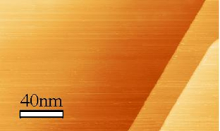
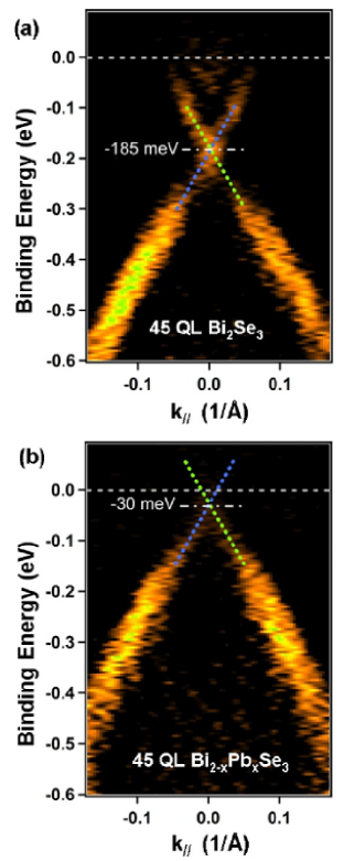
We use MBE to grow 45 QL Bi2Se3 films on bare insulating 6H-SiC (0001) substrates whose resistivity is cm, allowing us to neglect the conductance contribution from the substrate. A scanning tunneling microscope (STM) image of a typical film is shown in Figure 1. Atomically flat terraces with widths over 100 nm can be observed, with 1 quintuple layer thick terraces. Figure 2(a) shows the ARPES band map of a 45 QL Bi2Se3 film. A single Dirac cone is observed at the point, with the Dirac point located at 0.185 eV below the Fermi level. Hence, both the surface states and the bulk conduction band can contribute to electronic transport. The bulk chemical potential can be tuned inside the bulk energy gap by using appropriate dopants. Checkelsky2009 In this experiment, we accomplish this by doping the sample with Pb. Zhang2010b As shown in Fig. 2(b), after doping, the Fermi level of the Bi2-xPbxSe3 film is inside the energy gap. In this situation, the bulk conductivity is suppressed and the surface conductance becomes more evident.
The Bi2Se3 films were grown under Se-rich conditions on 6H-SiC (0001) substrates at 220∘C in an ultrahigh-vacuum (UHV) system (Omicron), equipped with MBE, STM and ARPES Zhang2010 . The base pressure of the system is Torr. High purity Bi (99.9999%) and Se (99.999%) were thermally evaporated from standard Knudsen cells. The temperatures of the Bi source and Se source are 550 and 170∘C. The Se4(Se2)/Bi flux ratio was between 10 and 15, which leads to a growth rate of QL min-1. In ARPES measurement, He-I (21.21 eV) photons produced by a Gammadata VUV 5000 discharging lamp and a Scienta SES2002 analyzer are used to excite and collect photoelectrons, respectively. All STM and ARPES data are taken at room temperature.
Subsequent to the ARPES analysis, the films were covered by 30 nm thick amorphous Se, which is quite insulating, as protective layers. Then, the samples were taken out from the UHV system for transport measurements in a variable temperature magnetocryostat with high magnetic field ( kOe) and low temperature ( K K) capability. Standard four probe electrical transport measurements were carried out using an ac resistance bridge with an excitation current of 500 nA. All resistance values were obtained by averaging over 50 measurements.
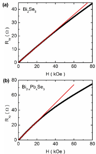
We determine the carrier density in the two samples using the Hall effect, as shown in Fig. 3. The carriers are electrons in both samples, and from the approximately linear behavior of at low magnetic fields, we estimate a carrier density of cm-3 ( cm-2) for the Bi2Se3 film and cm-3 ( cm-2) for the Bi2-xPbxSe3 film at 2 K. We estimate for Bi2Se3 and for Bi2-xPbxSe3, well within the diffusive transport regime. (The quantity is the elastic scattering length.) has a slightly non-linear behavior at high magnetic fields, which appears to be quite generic at low temperatures, and is likely an indication of more than one transport channel. Kong2010 ; Steinberg2010
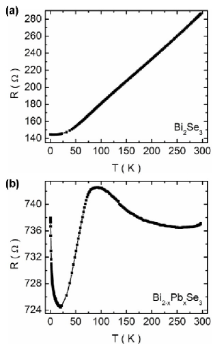
The temperature dependence of the sample resistivity in the range K K reveals a qualitative difference between the electrical properties of the two thin films. See Fig. 4 for the resistance vs temperature (R-T) plots for the two films from room temperature to 0.5 K. Above 50 K, the resistance of the Bi2Se3 film increases linearly with temperature, characteristic of the metallic behavior expected for a degenerately doped semiconductor. Its resistivity varies from 1.43 m cm at 297 K to 0.72 m cm at 500 mK. For the Bi2-xPbxSe3 film, the resistance is higher, with only a very weak, non-monotonic T dependence. Its resistivity is 3.69 m cm at both 297 K and 500 mK.
In an earlier studyButch2010 of a bulk Bi2Se3 system, it was found that the bulk remains conductive even for densities much smaller than those quoted above. The origin of the qualitative difference between our two thin films is not understood, but presumably has to do with the low-dimensional nature of our system, and also the fact that it has a much lower mobility than the system in Ref. Butch2010 .
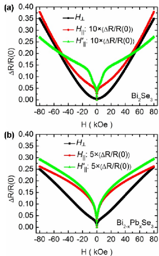
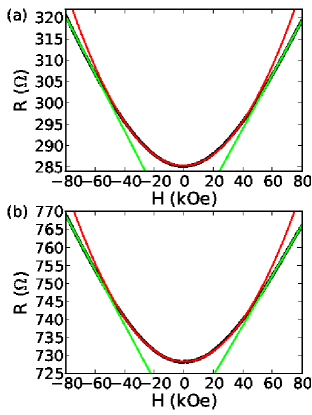
We have also measured the magnetoresistance for fields up to 80 kOe for three orientations of the magnetic field, as shown in Fig. 5. In the perpendicular field (), the fractional MR change, , between 80 and 0 kOe is about 35% for the Bi2Se3 film and 25% for the Bi2-xPbxSe3 film. When H is parallel to the film, the fractional MR change is much smaller, between 2.7% and 5.9%. Linear MR was observed above 10 kOe (30 kOe) when a perpendicular field was applied to the Bi2-xPbxSe3 (Bi2Se3) film as shown in Fig. 5(b). Such a linear MR has been attributed to the quantum linear MR of the surface states Tang2010 . We note that even at room temperature, the MR above 45 kOe has a better fit with a linear rather than parabolic dependence on the magnetic field for both samples (see Fig. 6). Upon closer inspection, the MR of the Bi2Se3 and Bi2-xPbxSe3 films shows sharp minima at zero field at low temperatures. These are better revealed in the Figure 7.
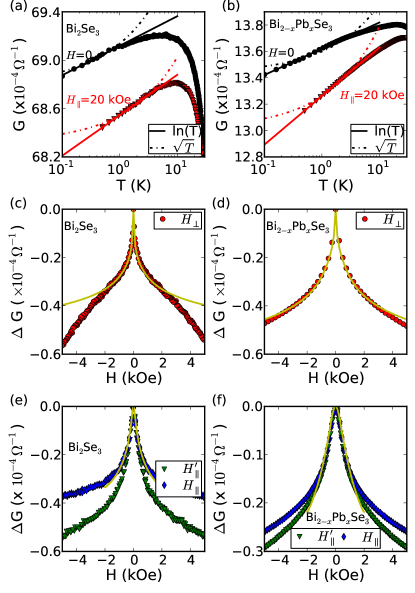
In the following, we focus on the behavior at low temperatures and low magnetic fields, because that is the most relevant parameter regime for our discussion within the context of quantum theories of localization. Figures 8(a) and (b) display the dependence of the conductance for zero magnetic field as well as for a 20 kOe in-plane field. The logarithmic behavior is suggestive of a weakly disordered 2D system where diffusive transport is determined by either weak localization or EEI. Figures 8(c) and 8(d) show the magnetoconductance as a function of a perpendicular field , while Figs. 8(e) and 8(f) show the magnetoconductance for the two directions of an in-plane field ( and ) as defined in the caption of Fig. 5. The observed magnetoconductance is negative, which is often referred to as weak antilocalization. In all cases, the magnetoconductance peak disappears at temperatures above 20 K, suggesting quantum correction as its origin.
III Analysis
III.1 Weak localization for noninteracting electrons
We first attempt to analyze these measurements using the standard results of weak localization (WL) theory for noninteracting electrons, and find that they are inconsistent with either 3D or 2D weak localization. The logarithmic temperature dependence of conductance rules out 3D behavior, because in 3D we expect , where is defined by the dependence of the phase coherence time . The exponent is dependent on the source of the inelastic scattering which causes the phase decoherence. For example, for phonon scattering, and (3D) or (2D) for the electron-electron interaction. In 2D, on the other hand, the correction to the conductivity at zero field is given by Hikami1980
| (1) |
where is a constant depending on the relative strengths of the spin-orbit and spin-flip (magnetic) scatterings. In the limit of weak spin orbit and magnetic scattering, one obtains ; in the limit of strong spin orbit scattering and weak magnetic scattering, one finds ; and when the magnetic scattering is strong, we have . The Hikami-Larkin-Nagaoka equation for magnetoresistance in perpendicular field is Hikami1980 ,
| (2) | |||||
where is the digamma function and is the inelastic scattering length. The positive slope of conductance vs. implies that our samples are in the limit of weak spin-orbit scattering (). However, positive implies positive magnetoconductance, which is qualitatively inconsistent with the observed anti-localization behavior.
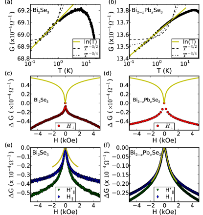
Figure 7 shows explicit comparison of the experimental results to the weak localization theory. The lines in Figure 7 (c-d) show the weak localization theory (Eq. (2) in the main text) for , as implied by the positive slopes of the data in Figure 7 (a-b). We have taken a typical value for the coherence length, nm. The lines in Figure 7 (e-f) are fits to the weak localization theory of Maekawa and FukuyamaMaekawa1981 in parallel field,
| (3) | |||||
where
| (4) | |||||
| (5) | |||||
| (6) | |||||
| (7) |
is the Zeeman g-factor, refers to the scattering time from disorder, and refers to the spin-orbit scattering in the directions perpendicular and parallel to the film. The source of the magnetic field dependence is the Zeeman splitting only, and this effect vanishes for . Roughly speaking, the factor is a measure of the comparative strengths of the spin orbit and elastic scattering. For example, if elastic scattering is strong (large ) compared to spin-orbit scattering, then this factor will be small. In the low-field limit, this equation gives , which is different from the observed sharp cusp. Nevertheless, as shown in Fig. 7(e) and (f), a very narrow parabola can be obtained for ; i.e. weak spin orbit scattering (). Although consistent with the temperature dependence, it is inconsistent with the expectation that the spin-orbit interaction in Bi2Se3 is strong.
III.2 Electron-electron interaction
Having shown that spin-orbit related WL alone cannot explain our data, we now examine the role of the dynamically screened EEI which also produces corrections to the conductivity. Again the logarithmic dependence rules out the 3D theory where we expect Lee1985 ; Lee1982 . On the other hand, the correction in 2D is
| (8) |
where is a function of the average of the static screened Coulomb interaction over the Fermi surface, . In 2D, . A non-zero magnetic field activates the large Zeeman splitting in Bi2Se3 Kohler1975 , introducing a further correction to the conductivity: Lee1985
| (9) |
where
| (10) |
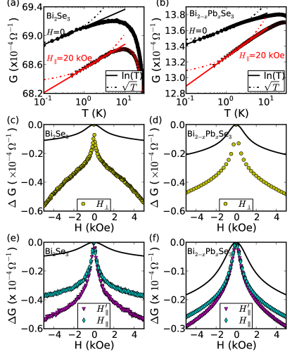
In Bi2Se3, the Zeeman -factor is 23 when is in-plane, and 32 when is out of plane Kohler1975 . When the Zeeman energy is much larger than , . At 20 kOe (red data shown in Figs. 9(a) and (b)), this limit is satisfied for K. The conductance is related to conductivity by a geometrical factor (e.g. length/width for a 2D surface) 1 for our samples.
Figure 8 shows a comparison of the data with the electron-electron interaction (EEI) theory. There are two fitting parameters, which are both obtained from the slopes of the lines in Figure 8 (a-b). These are the screening parameter, , and a geometrical factor relating the conductance with the conductivity, . In a wire with uniform current, is the ratio of cross-sectional area to length. We do not make this assumption, and instead use this factor as a parameter of the model. Using no further parameters, the EEI expressions correctly reproduce the signs of the and dependences, which already indicates the importance of EEI interactions. Although it does not capture the sharp peaks at zero field, the theory nicely reproduces all of the other qualitative features.
III.3 Combined weak localization and electron-electron interaction
We finally proceed to fit the experiment to the theory that contains corrections due to both weak localization and interaction. The temperature and H⟂ dependences in Figure 9(a)-(d) are fitted to the combined model, using the approximation , with , and taken as fitting parameters. (We take , as appropriate for 2D systems at sufficiently low temperatures where EEI is the dominant mechanism for dephasing.) The data were fitted in the range kOe2 kOe, which corresponds to the “low-field” region of the Bi2Se3 plot. We find (), () m, and () for Bi2Se3 (Bi2-xPbxSe3). The values for are slightly different from the value of expected from the strong spin-orbit interaction. The inelastic mean free paths are consistent with a previous measurement, m at 2 K Peng2010 .
The parameter , which incorporates the effect of interaction through , can be estimated from first principles. While our sample thickness is much smaller than the inelastic scattering length, making it two dimensional insofar as the weak localization correction to conductivity is concerned Lee1985 , the thickness is much larger than the Thomas Fermi screening length ( nm), suggesting that is to be estimated in a three-dimensional calculation. We will assume that to be the case. For the carrier densities reported above, a straightforward calculation using the Thomas-Fermi approximation for the interaction gives () and () for the Bi2Se3 and Bi2-xPbxSe3 films. For the calculation of we have assumed a three dimensional parabolic dispersion relation where ( is the charge of an electron) Kohler1974 . We have used the same dispersion for both samples, assuming that the doping has a negligible effect on the effective mass. (We note that if we had taken 2D screening with parabolic dispersion, we would get for 0.60 and 0.66, respectively. A 2D calculation assuming a Dirac cone with Fermi velocity m/s yields a calculated independent of the Fermi wave vector.) The fitted values of are smaller, suggesting that we are overestimating the strength of the interaction. This discrepancy is not understood, but is not surprising in view of the crudeness of our model; specifically, we neglect: the strong anisotropy of the effective mass (which can change by a factor of 8 between parallel and perpendicular directions Tichy ); doping dependence of the mass (which can change its value by as much as a factor of two Tichy ); and corrections to the mass due to quantum confinement in one direction.
We have also fit the data in parallel field, shown in Fig. 9(e-f). Since the theory does not allow for a difference between the two in-plane field directions, we have performed a simultaneous fit to both data sets. While the two data sets agree well at low fields, the disagreement at higher fields is not understood. In the limit of large spin-orbit scattering and low disorder, the predicted behavior cannot explain the sharp peak observed in the experiments. However, when the spin-orbit and disorder scattering times are comparable (roughly speaking, this occurs in the parameter range ), the weak localization model (Eqn. (3)) gives a good account of the observed behavior.
We note that there have been other experimental studies of thin films of TI materials Chen2010b ; He2010 ; Hirahara2010 . These do not identify the essential role of electron electron interactions. After the completion of this work we became aware of another article Liu2010 which studies transport in much thinner Bi2Se3 films (1-6 QLs) and interpret their results as indicating EEI as the origin of localization; their samples are not doped, however, and they also did not fit their data to EEI corrections discussed in the present article.
IV Conclusion
In conclusion, we have studied two thin film samples of the Bi2Se3, one of which has surface states with Fermi energy located in the conduction band, while the other has a Fermi energy within the bulk band gap because of Pb doping. We find a 2D WL theory combined with EEI fits the transport data of both samples very well. Note that the 2D WL model is relevant because the inelastic length in the these samples is much larger than the sample thickness, Lee1985 and does not in itself indicate transport in a surface state. Although ARPES results indicate that the surface states should play a role in the conductance of the doped sample, it is not possible at this stage to single out the contribution from the surface states. What we can conclude with confidence is that the electron-electron interaction, which has been neglected in most previous analyses, plays an essential role in quantum corrections to transport in thin films of TI Bi2Se3 material.
We acknowledge financial support from the Penn State MRSEC under NSF grant DMR-0820404 and by DOE under grant no. DE- SC0005042.
∗ These authors contributed equally to the project.
References and Notes
- (1) L. Fu, C. L. Kane, and E. J. Mele, Phys. Rev. Lett., 98, 106803 (2007).
- (2) J. E. Moore and L. Balents, Phys. Rev. B, 75, 121306 (2007).
- (3) R. Roy, Phys. Rev. B, 79, 195321 (2009).
- (4) X. L. Qi, T. L. Hughes, S. C. Zhang, Phys. Rev. B 78, 195424 (2008).
- (5) D. Hsieh et al., Nature (London) 460, 1101 (2009).
- (6) M. Z. Hasan and C. L. Kane, Rev. Mod. Phys., 82, 3045 (2010).
- (7) H. J. Zhang, C. -X. Liu, X. L. Qi, X. Dai, Z. Fang, and S. -C. Zhang, Nature Phys. 5, 438 (2009).
- (8) X. -L. Qi and S. -C. Zhang, Phys. Today 63, No. 1, 33 (2010).
- (9) J. G. Checkelsky et al., Phys. Rev. Lett., 103, 246601 (2009).
- (10) H. L. Peng et al., Nature Materials, 9, 225 (2010).
- (11) D. -X. Qu et al., Science, 329, 821 (2010).
- (12) N. P. Butch et al., Phys. Rev. B, 81, 241301(R) (2010).
- (13) P. Cheng et al., Phys. Rev. Lett., 105, 076801(2010).
- (14) Y. Zhang et al., Nature Phys., 6, 584 (2010).
- (15) P. A. Lee, and T. V. Ramakrishnan, Rev. Mod. Phys., 57, 287 (1985).
- (16) P. A. Lee, and T. V. Ramakrishnan, Phys. Rev. B, 26, 4009 (1982).
- (17) H. Köhler, and E. Wöchner, Phys. Status Solidi B, 67, 665 (1975).
- (18) Y. Zhang, et al., Appl. Phys. Lett., 97, 194102 (2010).
- (19) D. S. Kong et al., Nano Lett., 10, 329 (2010).
- (20) H. Steinberg, et al., Nano Letters, http://pubs.acs.org/doi/pdf/10.1021/nl1032183.
- (21) H. Tang et al., arXiv: 1003.6099v4.
- (22) S. Hikami, A. I. Larkin, and Y. Nagaoka, Prog. Theor. Phys., 63, 707 (1980).
- (23) S. Maekawa and H. Fukuyama, J. Phys. Soc. Jpn., 50, 2516 (1981).
- (24) H. Köhler and J. Kartmann, Phys. Status Solidi. B,63, 171 (1974).
- (25) L. Tichý and J. Horák, Phys. Rev. B, 19, 1126 (1979).
- (26) J. Chen et al., Phys. Rev. Lett., 105, 176602 (2010).
- (27) H. -T. He et al., arXiv: 1008.0141.
- (28) T. Hirahara et al. Phys. Rev. B, 82, 155309 (2010).
- (29) M. Liu et al. arXiv: 1011.1055 (2010).