APEnet+: a 3D toroidal network enabling Petaflops scale Lattice QCD simulations on commodity clusters
Abstract:
Many scientific computations need multi-node parallelism for matching up both space (memory) and time (speed) ever-increasing requirements. The use of GPUs as accelerators introduces yet another level of complexity for the programmer and may potentially result in large overheads due to the complex memory hierarchy. Additionally, top-notch problems may easily employ more than a Petaflops of sustained computing power, requiring thousands of GPUs orchestrated with some parallel programming model.
Here we describe APEnet+, the new generation of our interconnect, which scales up to tens of thousands of nodes with linear cost, thus improving the price/performance ratio on large clusters. The project target is the development of the APElink+ host adapter featuring a low latency, high bandwidth direct network, state-of-the-art wire speeds on the links and a PCIe X8 gen2 host interface. It features hardware support for the RDMA programming model and experimental acceleration of GPU networking. A Linux kernel driver, a set of low-level RDMA APIs and an OpenMPI library driver are available, allowing for painless porting of standard applications.
Finally, we give an insight of future work and intended developments.
1 Introduction
When we started our research on custom cluster interconnect back in 2003, we were at the beginning of the cluster revolution in a HPC arena which used to be dominated by custom supercomputers. Around that time, some seminal works [1] demonstrated the effective use of mainstream processors on Lattice QCD as well as on many other numerical problems. Not moving from the field of LQCD, another pioneering paper appeared some time afterward [2], showing that the same codes could be easily implemented on the newborn GPGPU architectures — with costs that didn’t deviate from those of, say, an ordinary PC workstation equipped with a medium/high-end video card —, displaying a substantial performance increase; research in this area is still progressing [3].
Today, to stay on a sustainable and green path towards the 10 Petaflops barrier, cluster systems are morphing into hybrid systems, starting from RoadRunner to current GPU accelerated systems. The TOP10 November 2010 list, the top 10 systems among the Top500 (www.top500.org), enlists 3 GPU accelerated clusters and, perhaps more significantly, 6 between custom and proprietary network interconnected systems. Today as seven years ago, we think that there is still room for innovation in the area of custom interconnection networks. Take for example a hypothetical 4 Petaflops GPU cluster — similar in performance to recently introduced GPU-based HPC systems; — it can be currently assembled out of 6000 GPU accelerated nodes, crammed into roughly 90-100 compute cabinets plus additional storage and communication cabinets. Connecting together 6000 nodes with current top-performing Infiniband QDR technology, e.g. using a full bi-sectional bandwidth tree, means building a multi-level fat tree of switches which easily imposes hard engineering problems — reliability, stability, etc.— and unexpectedly high costs, as high as 2000$ per port, properly accounting for the costs of the adapters, switches, cables both between cards and switches and between switches at different levels. Surprisingly, a high-performance interconnect can amount to 30-40% of the cost of a computing node.
Drawing on our past experience with the design of custom hardware for Lattice QCD HPC [4, 5, 6, 7], together with further developments in EU Framework Programme 6 project SHAPES [8, 9] we designed APEnet+, a new implementation of our 3D torus cluster interconnect [10, 11], based on the APElink+ adapter, which integrates both a network interface and a switching component 111This is commonly referred to as a direct network, as there is a packet switching component integrated into each network node, as opposed to traditional indirect networks like Ethernet and Infiniband, where switching capabilities are moved to dedicated hardware components.. The advantages of a torus network over a switched fabric network — i.e. Infiniband — are clear and well known: it naturally suits the transmission patterns of a broad range of numerical simulation codes that are parallelized using the domain decomposition approach (which is the case with our codes for LQCD). It is performant, its bi-sectional bandwidth being conserved when cluster size is scaled to large volumes. It grants linear scaling of costs without additional expenses, the unitary cost of the APElink adapter and three cables being the only factor.
The downside clearly lies in the additional number of cables, with the necessary planning for the routing of cables of assorted lengths, according to the distance they have to travel, i.e. inside or outside each cabinet. Additionally, a torus interconnect gradually degrades its performance as the application communication pattern gets more irregular — e.g. protein folding, fluid dynamics, etc.— In these cases, an initial pre-processing operation may be necessary to optimally map the problem onto the underlying interconnect.
2 The APEnet+ hardware
In this section, we introduce the APEnet+ interconnect, our low latency, high bandwidth direct network, supporting state-of-the-art link wire speeds and a PCIe X8 gen2 host connection. The APEnet+ project is based on the APElink+, an FPGA-based board, which is discussed in section 2.2.
On this network, the computing nodes — e.g. a multi-core CPU optionally paired with GPU — are arranged in a cubic mesh interconnected by point-to-point links to form a 3D torus; thus, each node has 6 bi-directional full-duplex communication channels, i.e. along the , , , , and directions. Packets have a fixed size envelope (header+footer) and are auto-routed to their final destinations according to wormhole dimension-ordered static routing, with dead-lock avoidance.
2.1 Architecture Outlook
A computing host can be equipped with one such board and made into a low latency, high bandwidth cluster node.
The APEnet+ architecture may be seen as a network of routers — see router component in Fig. 1 — with configurable routing capabilities operating on packets with payload of variable size.
The torus link block — see top part of Fig. 1 — manages the data flow by encapsulating the APEnet+ packets into a light, low-level, word-stuffing protocol able to detect transmission errors via CRC. It implements two virtual channels [12] and proper flow-control logic on each RX link block to guarantee deadlock-free operations.
The APElink+ network interface — see bottom part of Fig. 1 — has basically two main tasks:
-
•
On the transmit data path, it gathers data coming in from the PCIexpress port, fragmenting the data stream into packets which are forwarded to the relevant destination ports, depending on the requested operation.
-
•
On the receive side, it provides hardware support for the RDMA programming model, implementing the basic RDMA capabilities (PUT and GET semantics) at the firmware level.
A micro-controller — the NIOS II 32 bit embedded processor, which is a standard Altera® Intellectual Property — mainly helps in simplifying the implementation of the receive path.
2.2 The APElink+ card
The APElink+ card is the latest generation of the APElink hardware, leveraging the most recent advances in host interface technology, physical link speed and connector mechanics — see Table 1. — The APElink+ card is a single FPGA-based PCI Express board, representing a vertex of a 3D torus mesh network with 6 independent point-to-point multiple links channel (i.e. the links between mesh sites).
The employed FPGA device is the EP4SGX290 which is part of the Altera® 40 nm Stratix IV device family. This device is equipped with 36 full-duplex CDR-based transceivers, each supporting data rates up to 8.5 Gbps. Each link is made up of 4 bidirectional lanes bonded together with proper alignment logic.
High-level functions, like RDMA virtual-to-physical address tables look-up, are carried out by a program running on the FPGA embedded micro-controller (NIOS II) which uses the DDR3 module as both program- and data-memory.
The hardware block structure, depicted in Fig. 1, is split into a so called network interface — the packet injection and processing logic comprising PCIe, TX/RX logic, etc.— a router component and multiple torus links.
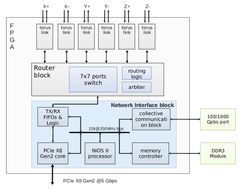
The torus links are 6 independent blocks with 2 virtual channel receive buffers needed for deadlock prevention. Proper flow control is maintained via credits handshake between a local RX block and the remote TX block, and it is embedded in the link protocol data layer. The torus link is autonomously able to re-transmit the header and the footer in case of transmission errors. Therefore the protocol assures the delivery of the packet avoiding nonrecoverable situations where badly corrupted packets (with errors in the header or footer) pose a threat to the global routing. Packets with payload errors (signaled by the footer) are handled at the software level. The chosen CRC polynomial generator is the industry-standard, well-known CRC-32.
The router comprises a fully connected, 7-ports-in/7-ports-out switch, plus routing and arbitration blocks. The routing block examines a packet header and resolves the destination address to a proper path across the switch. It supports the dimension-ordered routing algorithm, with a routing latency of 60ns.
The host interface, implemented as PCIe X8 gen2, allows communication between the host processor and the network.
| APElink | APElink+ | |
|---|---|---|
| FPGA component | Altera Stratix S30 | Altera Stratix IV GX 290 |
| # links | 6 | 4/6 |
| link technology | external National ser/des | embedded Altera transceivers |
| link cables | LVDS | QSFP+ standard |
| raw link speed | 6 Gbps | 34 Gbps |
| host interface | PCI-X 133MHz | PCIe X8 Gen2 |
| peak host BW | 1GB/s | 4+4GB/s |
Moreover, an Ethernet port is foreseen in order to build an additional, secondary network with an offload engine for collective communication tasks.
3 The APEnet+ software
All APEnet+ software is developed and tested on RedHat Enterprise Linux 5 and is available under the GNU GPL Licence. It spans across four major topics: the firmware software running on the FPGA embedded processor — the NIOS II processor in Fig. 1, — the linux kernel driver, the application level RDMA library and a MPI implementation. We developed a native APEnet+ BTL module for OpenMPI 1.X, implemented on top of the RDMA APIs.
The firmware software running on the FPGA embedded processor is currently in charge of managing the RDMA virtual-to-physical address translation table, but we are exploring new ways to exploit it for higher-level tasks.
For maximum performance, applications can use a set of low-level custom RDMA APIs, which is available as a C language library:
-
•
Communication primitives available to applications are: rmda_put(), rdma_get(), rdma_send().
-
•
Memory buffer registration primitives allow for exposing memory buffers to RDMA primitives: register_buffer(), unregister_buffer().
-
•
Events are routed to applications whenever RDMA primitives are executed by APEnet+: wait_event().
We are currently working [14] on the hardware and software features needed for GPU-initiated communications, e.g. providing a NVidia CUDA version of the rdma_put() primitive, using so called PCIe peer-to-peer transactions, in order to avoid intermediate copies onto CPU memory buffers. Along the same lines of overhead reduction, there is work underway for implementing RDMA events delivery — by the APElink+ hardware in CPU memory — accessible from within CUDA kernels.
Another research topic is exposing GPU memory areas as RDMA buffers, in such a way they can be target of RDMA PUT and GET operations, so cutting the latency of network operations. To this end, discussions are ongoing with some GPU vendors.
4 The deployment initiative
We are aggregating a small community of LQCD developers and users around our QUonG (lattice QUantum chromodynamics ON Gpus) deployment initiative.
The reference platform is a GPU-accelerated cluster with the following characteristics: a single enclosure system with at least 16 computing nodes, e.g. with a Torus topology. Each node is a dual-socket CPU system in a 1U enclosure with at least 2 X16 PCIexpress slots. One APElink adapter per CPU. One or two GPUs, possibly using separate enclosures — e.g. NVidia Tesla S2050. — The software environment is mainly OpenMPI or an hybrid OpenMP plus OpenMPI. Some optimized LQCD kernels will be provided, mainly consisting of the GPU optimized Wilson-Dirac kernel and a simple multi-node parallel solver.
5 Project status and future developments
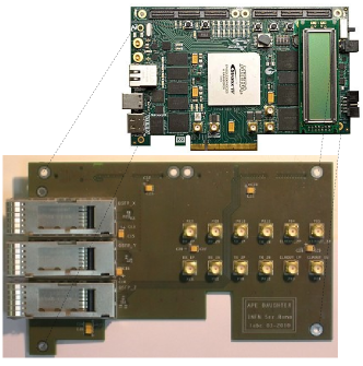
The APEnet+ hardware is at its final stages of development. A schematic view of the complete board is visible in Figure 2. Four links out of six are hosted on the main board, and two more, say and , are located in a small daughter-card on the upper level. In this way, the complete card occupies two PCI standard slots in a PC chassis, while it’s still possible to use it in a four-link and only one slot wide configuration. The prototypes will be available at beginning of 2011.
Meanwhile, a test system has been implemented in order to develop the FPGA firmware, the PCI Express interface and the physical layer interconnection technology. We used a commercial Altera® development kit (equipped with a smaller Altera® Stratix IV GX 230) and a custom-designed daughter-card (an HSMC mezzanine designed at LABE in INFN-Roma) hosting 3 QSFP+ connectors. This assembled system allows us to test the QSFP+ technology together with the embedded Altera® transceivers up to a bit rate of 24 Gbps for each link. Extensive electrical characterization is in progress ([13], [15] and more work yet to be published).
A first mini-cluster is being assembled together with GPUs and the APElink+ version with 3 links, for final validation of the firmware, the interconnection and the complete software stack on a small size (2-8 nodes). Synthetic tests, as well as real life simulations, will be performed by the end of 2010, so to be ready with the 6-links prototype release and eventually a bigger cluster deployment.
We thank the people in the Electronics Laboratory (LABE) in INFN-Roma, in particular Valerio Bocci, Giacomo Chiodi and Riccardo Lunadei.
This work was partially supported by the EU Framework Programme 7 project EURETILE under grant number 247846.
References
- [1] M. Lüscher, Lattice QCD on PCs? Nucl. Phys. Proc. Suppl. 106 (2002) 21 [arXiv:hep-lat/0110007].
- [2] G. Egri, Z. Fodor, C. Hoelbling, S. Katz, D. Nogradi and K. K. Szabo, Lattice QCD as a video game, Comput. Phys. Commun. 177 (2007) 631 [arXiv:hep-lat/0611022v2].
- [3] M. A. Clark, R. Babich, K. Barros, R. C. Brower and C. Rebbi, Solving Lattice QCD systems of equations using mixed precision solvers on GPUs, Comput. Phys. Commun. 181 (2010) 1517 [arXiv:0911.3191 [hep-lat]].
- [4] http://apegate.roma1.infn.it/APE
- [5] F. Bodin et al., The APENEXT project, Proceedings of Lattice2001 conference, Nucl.Phys.Proc.Suppl.106:173-176, 2002
- [6] R. Ammendola et al., Status of the apeNEXT project, Proceeding of Lattice2002 conference, Nucl.Phys.Proc.Suppl.119:1038-1040,2003.
- [7] F. Belletti et al., Computing for LQCD: apeNEXT, Computing in Science Engineering, 8, Jan-Feb, 18-29, 2006, [doi:10.1109/MCSE.2006.4].
- [8] P.S. Paolucci, A.A. Jerraya, R. Leupers, L. Thiele, and P. Vicini, Shapes: a tiled scalable software hardware architecture platform for embedded systems, Proceedings of the 4th international Conference on Hardware/Software Codesign and System Synthesis CODES+ISSS ’06 (Seoul, Korea), ACM Press, Pages 167-172, 2006.
- [9] P.S. Paolucci, P. Vicini et al., Introduction to the Tiled HW Architecture of SHAPES, Proc. Design, Automation and Test in Europe (DATE’07), Vol.1, Pages 77-82, France, Nice, April 2007.
- [10] R. Ammendola, M. Guagnelli,G. Mazza, F. Palombi, R. Petronzio, D. Rossetti, A. Rossetti, A. Salamon, P. Vicini, APENet: LQCD clusters a la APE, Proceedings of Lattice 2004 conference, Nucl.Phys.B - Proc.Suppl.140:826-828, March 2005 [arXiv:hep-lat/0409071v1].
- [11] R. Ammendola, R. Petronzio, D. Rossetti, A. Salamon, N. Tantalo and P. Vicini, Status of the APENet project, Proceedings of Lattice2005 conference, \posPoS(LAT2005)100.
- [12] W.J. Dally and C.L. Seitz, Deadlock-Free Message Routing in Multi- processor Interconnection Networks, IEEE Trans. Comput. 36 (1987) 547-553
- [13] R. Ammendola et al., High Speed Data Transfer with FPGAs and QSFP modules, to be published on Journal of Instrumentation (JINST)
- [14] R. Ammendola et al., Mastering Multi-GPU Computing on a Torus Network, poster at NVidia GPU Technology Conference 2010, San Jose (CA).
- [15] R. Ammendola et al., APEnet+: high bandwidth 3D torus direct network for petaFLOPS scale commodity clusters, to be published on Journal of Physics: Conference Series (JPCS)