Polytypic nanowhiskers: electronic properties in the vicinity of the band edges
Abstract
The increasing interest of nanowhiskers for technological applications has led to the observation of the zinc-blend/wurtzite polytypism. Polytypic nanowhiskers could also play, by their characteristics, an important role on the design of optical and electronic devices. In this work we propose a theoretical model to calculate the electronic properties of polytypic zinc-blend/wurtzite structure in the vicinity of the band edges. Our formulation is based on the method connecting the irreducible representations in the interface of the two different crystalline phases by group theory arguments. Analyzing the composition of the states in the point and the overlap integrals of the envelope functions we predict energy transitions that agree with experimental photoluminescence spectra.
I Introduction
Recently an increasing number of papers have reported high quality and control growth of nanowires and nanowhiskers (NWs) of III-V compounds such as InP, InAs, GaAs and GaP Bao et al. (2009); Johansson et al. (2007, 2005); Caroff et al. (2009); Tchernycheva et al. (2007); Kitauchi et al. (2010); Ihn et al. (2007). Nanoelectronics, nanophotonics and solar cells are some of the technological applications for these nanostructures like described in the references above.
Vapor-liquid-solid (VLS) method Wagner and Ellis (1964) was used, in 1964, by Wagner and Ellis to grew a silicon whisker. Since then, other methods like molecular beam epitaxy (MBE) and metal organic vapor phase epitaxy (MOVPE) have also been applied to the growth of NWs. These techniques allow the fabrication of homo and heterostructures in both axial and radial directions opening new opportunities to engineering novel device applications.
A heterostructure is composed by assembling different materials side-by-side along a growth direction. The homostructure is a similar concept, however, it is not the kind of material that is different but its crystalline structure. This effect is also known as polytypism and have been observed in NWs structures of several III-V compounds.
Under standard temperature and pressure conditions, the III-V compounds have as the bulk stable phase the zinc-blend (ZB) structure, exception made for the nitrides that have the wurtzite (WZ) structure as the most stable phase. However, reducing the dimensions to the nanoscale level such as in these NWs, the WZ phase has been observed for non-nitride III-V compounds. The natural explanation to this behavior is the small formation energy difference between the two crystal structures.
The phase alternation creates ZB and WZ regions along the growth direction affecting the NWs optical and electronic properties, generating new forms of band offsets and electronic minibands that can be explored to produce new kinds of applications.
The WZ/ZB polytypism in III-V compounds can make a type II homostructure characterized by a staggered band-edge lineup, i. e., the charge carriers are spatially separated: the electrons will be concentrated in the ZB region while the holes will be in the WZ region. A summary of NWs growth, properties and applications was made by Dubrovskii et al. Dubrovskii et al. (2009).
From the theoretical point of view, the literature about these III-V NW structures, is focused in growth stability, surface energies and formation of polytypism Glas (2008); Sano et al. (2007); Akiyama et al. (2006); Moreira et al. (2010); Sibirev et al. (2010); Nastovjak et al. (2010); Lubov et al. (2009). Only recently theoretical calculations of the electronic properties in the band edges have been done for such structures Gadret et al. (2010). None has been done in the vicinity of the band edges.
The polytypism was investigated in a paper of Murayama and Nakayama Murayama and Nakayama (1994) by ab initio calculations of the band offsets in WZ/ZB interfaces. A useful schematics of the correspondence between the symmetry of the states of the WZ and ZB structures has been presented in the same article.
The aim of this study is to propose a theoretical model based on group theory arguments and the method to calculate the electronic band structure in the vicinity of the band edges and envelope functions of a WZ/ZB/WZ homostructure for indium phosphide (InP). The effective mass parameters for the WZ bulk phase of InP were extracted from a paper by Pryor and De De and Pryor (2010) that predicted the band structures of some III-V bulk compounds in the WZ phase (phosphides, arsenides and antimonides). The ZB parameters are extracted from Vurgaftman et al. Vurgaftman et al. (2001).
The formulation of a theoretical model for this new kind of nanostructures can lead to band gap engineering and novel electronic a and also work as a guide for the crystal growth community.
II Theoretical model
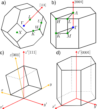
The existence two different crystal phases in a single whisker, can be explained by a simple joint analysis of the ZB and WZ crystal structures. Looking into ZB along the [111] direction and to WZ along the [0001] direction, one can found a noticeable similarity. Both can be described as stacked hexagonal layers. In fact, the ZB structure has three layers in the stacking sequence (ABCABC) while the WZ structure has only two (ABAB). So, a stacking fault in WZ becomes a single segment of ZB and two sequential twin planes in ZB form a single segment of WZ Caroff et al. (2009).
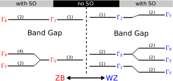
An important difference between the two structures is the crystal field energy present in the WZ structure that defines the top of the valence band, neglecting spin, as a composition of two different bands, a non-degenerate and a bidegenerate bands. In ZB, the top of valence band is composed by a three-degenerate band. This difference in the energy bands between the two structures can be seen schematically for the point in figure 1, with and without the spin-orbit interaction.
To calculate the band structure of a polytypic NW based in the matrix formalism, it is necessary to understand the differences between the two crystal structures in the reciprocal lattice or, more precisely, what happens with the high-symmetry points in the ZB first Brillouin zone when we are dealing with the [111] growth direction and how they can be related to the WZ ones.
Looking through the [111] axis in figure 2a one can see that the point of ZB structure is projected in the point. Since the number of atoms in the primitive unit cell for WZ is twice the number in ZB, there are more states in the point of WZ. This correspondence is done by assigning and points of the ZB to the point of WZ. This compatibility can be seen in the energy diagram presented by Murayama and Nakayama Murayama and Nakayama (1994), that relates the irreducible representations of the ZB and points to the WZ point. This energy diagram provides the essential insight for our method since we are going to relate matrices developed with irreducible representations belonging to different crystal structures.
The usual matrix formulation is constructed in the vicinity of the point for ZB and WZ structures Kane (1966); Chuang and Chang (1996) considering the first three valence bands and the first conduction band, represented by a matrix. When the spin-orbit interaction is included this number is multiplied by 2, resulting in a matrix. These bands are exactly the ones presented in figure 1, and represent a smaller set of the states first presented by Murayama and Nakamura Murayama and Nakayama (1994). Analyzing this, one may notice that, in the present method the irreducible representations of ZB [111] belong only to the point and no irreducible representation of the point will appear in the formulation.
Another subject, asides the symmetry correspondence, must be pointed out: the matrix for the ZB structure is developed for the cubic main axes, which are the [100], [010] or [001] growth direction. This implies that the definition of the coordinate system defines the matrix representations of the symmetry operations used to calculate the matrix elements in the formulation. Changing the coordinate system to , which is the coordinate system of the WZ Hamiltonian, will enable us to relate the ZB and WZ matrices.
We can either recalculate the matrix representations of the symmetry operations and develop the ZB matrix or use the rotation matrices presented in the paper of Park and Chuang Park and Chuang (2000) to transform the ZB Hamiltonian in the to the coordinate system.
The basis, , in the prime coordinate system is defined as (from this point on, the prime will be dropped out of the notation):
| (1) |
which is convenient to describe the WZ Hamiltonian.
Since we are not treating the interband interaction explicit in the matrix, the conduction band have a parabolic form for both crystals and is not affected by the rotation, reading as
| (2) |
where is the gap energy, is the energy of the top valence band and for the ZB structure the electron effective masses are the same .
Applying the rotation matrices to the valence band ZB Hamiltonian we obtain a common matrix for the two structures:
| (3) |
The matrix terms are defined as:
| (4) |
where .
The only difference from the usual WZ formulation is the inclusion of a new parameter, , that takes into account the reorientation of the ZB growth axis.
The and WZ parameters can be related to the and ZB parameters comparing the ZB rotated matrix to the WZ matrix.
In this work we will assume the WZ as ideal and therefore the lattice parameters will considered the same as ZB. As a consequence, strain effects will not be taken into account.
III Results and discussion
We first apply our model for bulk ZB and WZ InP to check the reliability of the matrix for both crystal structures. This initial investigation is useful to fit the effective mass parameters and to understand the valence band states in the band edge since now we are dealing with different basis states for the ZB matrix.
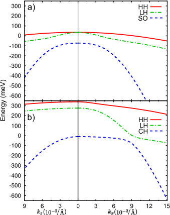
The ZB parameters were obtained from Ref. Vurgaftman et al. (2001) and the WZ parameters were derived using the effective masses presented in Ref. De and Pryor (2010). Since in our model there is no explicit interband interaction only the valence band is presented in figure 3 for the bulk form of both crystal structures.
The usual identification of the bands were used for ZB while in WZ we had to analyze the composition of the states in the point. Table 1 summarizes the energies and states compositions in the point that helps us to identify the WZ states.
| Energy | Set of states 1 | Set of states 2 |
|---|---|---|
The energies and the and coefficients are given by Chuang and Chang (1996):
| (5) |
| (6) |
| (7) |
| (8) |
| (9) |
The states identification were made as described in Ref. Chuang and Chang (1996): HH (heavy hole) states are composed only by or , LH (light hole) states are composed mainly of or and CH (crystal-field split-off hole) are composed mainly of or . According to the identification of the energies presented in table 1, is the HH state and, if , is the LH state and is the CH state or is the CH state and is the LH state otherwise. The valence band ordering in the point, which depends on the values of , and , and the value of the coefficients for both crystal structures can be found in table 2.
| Energies | |||
|---|---|---|---|
| ZB | 0.57735 | 0.81650 | |
| WZ | 0.98345 | 0.18116 |
Since in our model we are using the WZ basis to describe the ZB structure it is useful to think that ZB is a WZ structure with zero crystal-field energy. Noting this feature we can identify the ZB valence band states in the point using the WZ identification. This helps us to understand the band edge in the WZ/ZB interface in a quantum well structure. Table 3 relates the two different identifications.
| ZB identification | WZ identification |
| HH | HH |
| LH | CH |
| SO | LH |
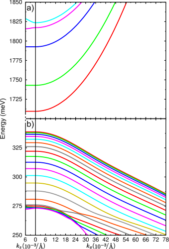
As the dimensions of NWs are big enough to avoid lateral confinement, this structure can be considered as a 2-dimensional system, like a quantum well or a superlattice. In this context, we simulated a single WZ/ZB/WZ polytypic quantum well with well width and barrier width so that the whole system has .
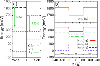
Using the band mismatch value given in Ref. De and Pryor (2010) it is possible to construct the quantum well profile. To understand the confinement profile we plotted, in figure 4a, the band edge energy in the WZ/ZB interface. Since the composition of the states LH and CH is different in both crystal structures we did not think it was convenient to draw a line connecting the energies. We believe that there’s a mix of these values to form the effective potential. However, we can note that the conduction band and the first valence band form a type-II homostructure.
It is also convenient to plot the diagonal terms of the total Hamiltonian to check the variation of the parameters along the growth direction, which can be found in figure 4b. Although the nondiagonal terms of the matrix will mix the three profiles we can expect that the confinement of the electrons will be in the ZB region while the holes will be in the WZ region belonging in their most to the HH state.
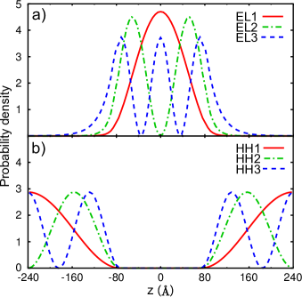
The band structure of the quantum well plotted up to 10% of the direction and 100% of the direction is shown in figure 5. We can observe that the bound states in the valence band are mainly HH states, which means they are composed entirely by the and states of the basis that have only and components. This feature directly reflects in the luminescence properties of the system: the light will be almost fully polarized in the plane, i. e., transversal to the growth axis of the polytypic quantum well. The LH states have less than 5% of component.
The probability densities calculated from the envelope functions for the point of the EL1, EL2, EL3, HH1, HH2 and HH3 bands are shown in figure 6. These results agrees with the experimental data suggesting a spatial separation of the carriers, due to the fact that is more likely to find holes in the WZ region and electrons in the ZB region.
In a quantum well the selection rules for dipole optical transition are given by the matrix element Fox (2001).
| (10) |
This matrix element can be divided in two parts: and . is the matrix element between the electron and hole states in the basis that depends on the polarization of the light and is the overlap integral between the electron and hole envelope functions.
| (11) |
| (12) |
The matrix elements are known from symmetry properties of the point and the non-vanishing elements are , and . We just have to calculate the overlap integral . Since the potential profile is even, the envelope functions have well defined parities, they are either even or odd and we can expect to have null overlap integrals between conduction and valence states. The non-zero overlap integrals and the difference energy in the point are presented in table 4.
| (%) | Energy difference (meV) | |
|---|---|---|
| EL1-HH1 | 2.6 | 1370.76 |
| EL1-HH3 | 6.4 | 1372.89 |
| EL2-HH2 | 12 | 1405.06 |
| EL3-HH1 | 23 | 1453.86 |
| EL3-HH3 | 33.5 | 1455.99 |
Although we have achieved reliable results with the model considered here for InP, we believe that improvements should be made to treat other III-V compounds. In systems where the lower conduction band has symmetry in the WZ phase and the spin-orbit splitting is bigger or equivalent to the gap energy (InAs and InSb De and Pryor (2010)) the full method should be considered with the inclusion of the Kane interband momentum matrix elements () and also Kane quadratic terms (). In systems with symmetry in the lower conduction band for WZ phase, like AlAs or GaAs De and Pryor (2010), the full symmetry analysis should be redone.
IV Conclusions
In summary, we have presented a theoretical method based in group theory arguments and the method to calculate the electronic properties of InP polytypic structures in the vicinity of the band edges.
Understanding the behavior of the band structure of the calculated system we could predict the trends in the luminescence energy transitions. The preliminary results are in good agreement with the experimental data available so far such as carriers’ spatial separation and light polarization in luminescence spectra.
With the proposed model, it will be possible to predict the optical properties of selected structures and to design systems that best fit new device applications.
V Acknowledgements
We like to thank the Brazilian funding agencies CAPES and CNPq for the financial support.
References
- Bao et al. (2009) J. Bao, D. C. Bell, F. Capasso, N. Erdman, D. Wei, L. Froberg, T. Martensson, and L. Samuelson, Advanced Materials, 21, 3654 (2009).
- Johansson et al. (2007) J. Johansson, L. S. Karlsson, C. P. T. Svensson, T. Mårtensson, B. A. Wacaser, K. Deppert, L. Samuelson, and W. Seifert, Journal of Crystal Growth, 298, 635 (2007).
- Johansson et al. (2005) J. Johansson, L. S. Karlsson, C. P. T. Svensson, T. Martensson, B. A. Wacaser, K. Deppert, L. Samuelson, and W. Seifert, Nature Materials, 5, 574 (2005).
- Caroff et al. (2009) P. Caroff, K. A. Dick, J. Johansson, M. E. Messing, K. Deppert, and L. Samuelson, Nature Nanotechnology, 4, 50 (2009).
- Tchernycheva et al. (2007) M. Tchernycheva, G. E. Cirlin, G. Patriarche, L. Travers, V. Zwiller, U. Perinetti, and J.-C. Harmand, Nano Letters, 7, 1500 (2007).
- Kitauchi et al. (2010) Y. Kitauchi, Y. Kobayashi, K. Tomioka, S. Hara, K. Hiruma, T. Fukui, and J. Motohisa, Nano Letters, 10, 1699 (2010).
- Ihn et al. (2007) S.-G. Ihn, J.-I. Song, Y.-H. Kim, J. Y. Lee, and I.-H. Ahn, Nanotechnology, IEEE Transactions on, 6, 384 (2007).
- Wagner and Ellis (1964) R. S. Wagner and W. C. Ellis, Applied Physics Letters, 4, 89 (1964).
- Dubrovskii et al. (2009) V. Dubrovskii, G. Cirlin, and V. Ustinov, Semiconductors, 43, 1539 (2009).
- Glas (2008) F. Glas, Journal of Applied Physics, 104, 093520 (2008).
- Sano et al. (2007) K. Sano, T. Akiyama, K. Nakamura, and T. Ito, Journal of Crystal Growth, 301-302, 862 (2007).
- Akiyama et al. (2006) T. Akiyama, K. Sano, K. N. Akamura, and T. Ito, Japanese Journal of Applied Physics, 45, L275 (2006).
- Moreira et al. (2010) M. D. Moreira, P. Venezuela, and R. H. Miwa, Nanotechnology, 21, 285204 (2010).
- Sibirev et al. (2010) N. Sibirev, M. Timofeeva, A. Bol′shakov, M. Nazarenko, and V. Dubrovskii, Physics of the Solid State, 52, 1531 (2010).
- Nastovjak et al. (2010) A. Nastovjak, I. Neizvestny, I. Shwartz, and Z. Yanovitskaya, Semiconductors, 44, 127 (2010).
- Lubov et al. (2009) M. Lubov, D. Kulikov, and Y. Trushin, Technical Physics Letters, 35, 99 (2009).
- Gadret et al. (2010) E. G. Gadret, G. O. Dias, L. C. O. Dacal, M. M. de Lima Jr., C. V. R. S. Ruffo, F. Iikawa, M. J. S. P. Brasil, T. Chiaramonte, M. A. Cotta, L. H. G. Tizei, D. Ugarte, and A. Cantarero, Physical Review B, 82, 125327 (2010).
- Murayama and Nakayama (1994) M. Murayama and T. Nakayama, Phys. Rev. B, 49, 4710 (1994).
- De and Pryor (2010) A. De and C. E. Pryor, Physical Review B, 81, 155210 (2010).
- Vurgaftman et al. (2001) I. Vurgaftman, J. R. Meyer, and L. R. Ram-Mohan, Journal of Applied Physics, 89, 5815 (2001).
- Kane (1966) E. O. Kane, Physics of III-V compounds vol. 1, edited by R. K. Willardson and A. C. Beer, Semiconductors and Semimetals, Vol. 1 (World Scientific, 1966) Chap. 3, pp. 75–100.
- Chuang and Chang (1996) S. L. Chuang and C. S. Chang, Physical Review B, 54, 2491 (1996a).
- Park and Chuang (2000) S. H. Park and S. L. Chuang, Journal of Applied Physics, 87, 353 (2000).
- Chuang and Chang (1996) S. L. Chuang and C. S. Chang, Applied Physics Letters, 68, 1657 (1996b).
- Fox (2001) M. Fox, Optical Properties of Solids, Oxford Master Series in Condensed Matter Physics (Oxford University Press, c2001) Chap. 6, pp. 115–142.