Direct correlation of crystal structure and optical properties in wurtzite/zinc-blende GaAs nanowire heterostructures
Abstract
A novel method for the direct correlation at the nanoscale of structural and optical properties of single GaAs nanowires is reported. Nanowires consisting of 100% wurtzite and nanowires presenting zinc-blende/wurtzite polytypism are investigated by photoluminescence spectroscopy and transmission electron microscopy. The photoluminescence of wurtzite GaAs is consistent with a band gap of 1.5 eV. In the polytypic nanowires, it is shown that the regions that are predominantly composed of either zinc-blende or wurtzite phase show photoluminescence emission close to the bulk GaAs band gap, while regions composed of a nonperiodic superlattice of wurtzite and zinc-blende phases exhibit a redshift of the photoluminescence spectra as low as 1.455 eV. The dimensions of the quantum heterostructures are correlated with the light emission, allowing us to determine the band alignment between these two crystalline phases. Our first-principles electronic structure calculations within density functional theory, employing a hybrid-exchange functional, predict band offsets and effective masses in good agreement with experimental results.
pacs:
78.55.Cr,68.37.Og,61.72.Mm,78.67.Uh,71.15.MbI Introduction
Semiconductor nanowires are attracting increasing interest because of their exciting optical and electronic properties and the possibility of synthesizing them in a controllable fashion Cui and Lieber (2001); Samuelson et al. (2004); Cui et al. (2003); Bjork et al. (2002). They are considered promising building blocks for the next generation of optical, sensing, electronic and energy harvesting devices Wang et al. (2005); Duan et al. (2001); Chan et al. (2008); Tian et al. (2007). Their small diameters, often at distances a few times the inter-atomic spacing in crystals, and their unique geometries lead to physical properties which differ significantly from the corresponding bulk material. Furthermore, nanowires hold the promise of integrating lattice-mismatched crystals on a single device, which opens new design possibilities and has the potential to significantly decrease production costs in solar cell applicationsKayes et al. (2005).
The functionality of nanowires is increased, and their properties are modified, when radial or axial heterostructures are created within a single wireLauhon et al. (2002); Gudiksen et al. (2002). Radial heterostructures can be produced by growing different materials on the side facets of the nanowires Fontcuberta i Morral et al. (2008); Heigoldt et al. (2009), while axial heterostructures correspond generally to a variation in the chemical composition along the growth axisBjork et al. (2002); Samuelson et al. (2004); Heiß et al. (2009). Recently, a second type of axial heterostructure has attracted attention, where the crystalline structure varies along the growth axis while the chemical composition is conserved. Typically, the structure is changed from the cubic zinc-blende to the hexagonal wurtzite structure Ross (2009); Caroff et al. (2009); Algra et al. (2008). This change of crystalline structure has been observed in some bulk materials such as SiC and GaN Park et al. (1994); Strite and Morkoc (1992). In phosphides and arsenides, it has been shown that the appearance of wurtzite phase is restricted to the nanowire form and is never observed in the bulk Davidson et al. (2007). The change in crystal structure is accompanied by changes in the electronic structure; for example, earlier theoretical work predicted a type II band alignment between the zinc-blende and wurtzite phases in III-V semiconductors Murayama and Nakayama (1994).
Recently, type II band alignment in InP nanowires Bao et al. (2008); Pemasiri et al. (2009) has been demonstrated allowing the formation of crystal phase qantum dots Akopian et al. (2010). Meanwhile the band structure of wurtzite GaAs has been a subject of controversy in the last few years. Recent works on the luminescence of GaAs nanowires with a high percentage of wurtzite phase show a large variety of results. Recently luminescence of wurtzite GaAs in the range of 1.53-1.54 eV has been reported Hoang et al. (2009). Previously, Martelli et al. had reported an emission at 1.522 eV in wurtzite GaAs nanostructures Martelli et al. (2007). Meanwhile Moewe et al. reported an emission at 10 meV below the zinc-blende GaAs band gapMoewe et al. (2008). Additionally, our own results presenting a mixture of wurtzite and zinc-blende phases in nanowires are consistent with a type II band alignment and smaller band gap Spirkoska et al. (2009). Indeed in nanowires presenting 30% and 70% wurtzite phase we have observed extremely sharp peaks 1.43 and 1.515 eV Spirkoska et al. (2009). The spectra could be explained by the existence of quantum heterostructures forming a type II band alignment Spirkoska et al. (2009). Additionally similar results have been obtained by other groups Akopian et al. (2010). We believe that the apparent contradictions of some of these literature results can be related to the fact that the optical and structural characterizations were not performed on the same nanowire. This limits the possibilities to account for variability in the structure of different nanowires from one growth. In this work we will perform a direct correlation between the structural and optical properties in order to overcome this limitation.
To the best of our knowledge, a direct correlation between the optical properties and the structural sequence in the polytypism, which requires both functional and structural characterization on the the same nanowire, has not yet been demonstrated Ropers et al. (2007). An initial effort in this direction was carried out by Bao et al. Bao et al. (2008) who looked at the shift of the luminescence band as a function of the excitation power for highly twinned and twin-free zinc-blende structures in InP nanowires. Arbiol et al. Arbiol et al. (2009) demonstrated by in-situ local electron energy loss spectroscopy (EELS) measurements on [111] zinc-blende inclusions in [0001] wurtzite nanowires in GaN the variation in the local density of states close to the band gap. Finally in different type of heterostructures, transmission electron microscopy (TEM) based cathodoluminescence was used to characterize GaN/InGaN/AlGaN nanowire heterostructures Lim et al. (2009). This technique enabled the direct correlation between the structural quality and and the carrier recombination characteristics in InGaN quantum wells Lim et al. (2009).
In this work, we provide a study that demonstrates direct correlation between the optical properties and structure at the atomic scale of GaAs nanowires formed by either pure wurtzite-GaAs or a combination of various thicknesses of the zinc-blende and wurtzite phases. This enables us to elucidate the band alignment between the two crystalline phases and represents an important step towards structural band gap engineering.
II Experimental Details
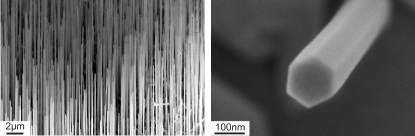
The nanowires were grown in a Gen II Molecular Beam Epitaxy (MBE) system. Wurtzite GaAs nanowires were grown by using gold as a catalyst, while the polytypic GaAs nanowires were obtained by the gold-free gallium-assisted growth method. In order to avoid cross-contamination because of the use of gold, the two different samples were fabricated in separate MBE systems. The nanowires with 98-100% wurtzite GaAs were grown on GaAs (11)B substrates at a growth temperature of 540 under a As4 Beam flux of mbar at a Ga rate equivalent to a planar growth of 0.8 Å/s. The growth time was 7500 s. The nucleation and growth followed the Vapor-Liquid-Solid mechanism, with Au as catalystWagner and Ellis (1964). Details on the growth procedure are described in Rudolph et al. (2009). After the axial growth of the nanowires the growth parameters were changed to conditions suitable for planar growth and the nanowires were passivated by an epitaxial prismatic shell of AlGaAs/GaAs material Heigoldt et al. (2009); Fontcuberta i Morral et al. (2008). The 2D equivalent amount grown during capping was 60 nm AlGaAs followed by 30 nm GaAs.
Wurtzite/zinc-blende polytypic nanowires were obtained on (11)B GaAs substrates previously coated with 20 nm SiO2. The growth temperature was C and the As beam flux at the beginning of the growth process mbar at a Ga rate equivalent to a planar growth of 0.22 Å/s. For this sample, the As beam flux increased slightly up to approx. mbar during the growth. The nanowires were capped by an epitaxial shell of AlGaAs/GaAs Heigoldt et al. (2009); Fontcuberta i Morral et al. (2008).
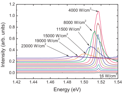
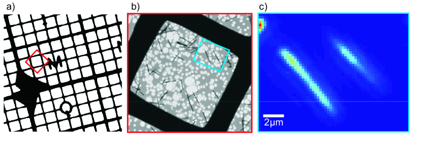
For the direct correlation experiments, the nanowires were first transferred onto TEM holey carbon Cu grids. The grids presented markers in order to facilitate the localization of the nanowires in the multiple measurements, see Fig. 1a-b. For the optical characterization, the grids were fixed freely suspended to a sample holder mounted in a confocal micro-photoluminescence (PL) setup. The sample stick was then immersed in a liquid helium bath cryostat. In order to ensure a good thermal dissipation during the optical measurements, the sample space was filled with a helium exchange gas at a pressure of 5 mbar. The measurements were carried out at a temperature of 4.2 K. The excitation sources were a semiconductor laser diode emitting at nm or a helium neon laser emitting at 632.8 nm. The laser was focused to a diffraction limited spot of about 0.8 m in diameter. This diffraction limit of light of the confocal microscopy is also the limiting factor for the overall resolution of the correlation technique. Typical excitation power densities were in the order of 10-50 W/cm2, orders of magnitude below the level where significant heating of the sample could be observed (Fig. 2). Indeed, in contrast to similar experiments performed in a helium flow cryostat Bao et al. (2008), we did not observe any severe heating effects resulting from the low heat conductivity of the thin carbon membrane. In our case, we are able to realize measurements on nanowires dispersed to a free-standing carbon membrane without the need of adding supplementary layers on top to allow for thermal dissipation as it was realized in previous studies Bao et al. (2008). Only this configuration enables simultaneous high resolution TEM and measurements on the same single nanowire. The position of the sample in the in the focal plane of the objective was verified by acquiring a confocal reflectivity image from the sample area. The measurements were then acquired by scanning an area of 20 m/side with a step of 250 nm and aquiring a spectrum at each position, see Fig. 1c. The spatial dependence of PL spectra along the nanowire axis was obtained by plotting the suitable cross-section of this dataset.
Right after measurements the nanowires were studied by TEM. A series of connected bright field HRTEM micrographs was obtained from the bottom to the top of the nanowire, with the purpose of obtaining detailed information on the structure. Both high resolution and low resolution measurements were taken. The micrographs were taken along the nanowire, ensuring that the ends were overlapping with the previous/following micrographs. Multiple subsequent micrographs was necessary to map the whole length. The electron microscopy (TEM and HRTEM) measurements were carried out in a CM300 LaB6 microscope with a point to point resolution of 0.17 nm.
III Results
III.1 Wurtzite GaAs band gap
We start by presenting results in nanowires consisting of nearly 100% wurtzite. In this case, the direct correlation method is less important, as there is no significant variation on the structure along the nanowire. The correlation allows us to verify that the photoluminescence characteristics are correctly attributed to nanowires composed from wurtzite GaAs.
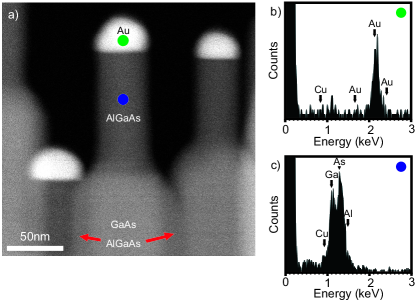
Fig. 3a shows a high angle annular dark field (HAADF) STEM micrograph of several nanowires from the sample. In principle the HAADF detector directly gives a contrast proportional to the atomic charge Z of the nuclei in the sample. The contrast also depends on the sample thickness that is not uniform in the axial extension compared to the rest of the wire. The image contrast in Fig. 3a therefore cannot directly indicate the chemical composition. For this reason energy dispersive X-ray spectroscopy (EDX) was performed at the thin extension and the catalyst droplet to clearly determine the chemical composition. Fig. 3b shows the EDX spectrum taken with the electron beam focused at the tip of the nanowire. The spectral features clearly demonstrate the presence of the Au catalyst. Meanwhile Fig. 3c shows that the thin extension of the nanowire towards the tip corresponds to axially grown AlGaAs. This is in clear agreement with the picture that during the radial capping with the AlGaAs/GaAs shell the nanowire continues to grow axially from precipitation below the catalyst droplet. Indeed for the case of Au catalyzed nanowire the metallic catalyst is not affected by the growth conditions. We can therefore use the size of the nanowire neck to accurately estimate the size of the nanowire core.
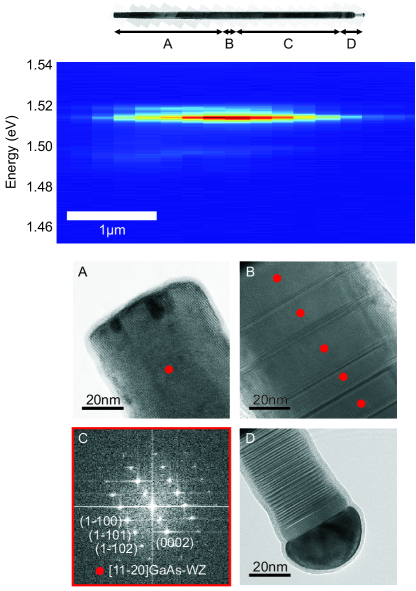
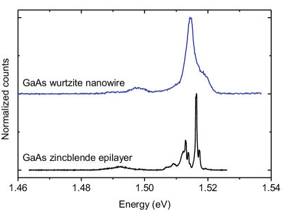
Now we turn to the correlation between HRTEM and spatial dependent PL. In Fig. 4 we have included TEM micrographs representative of various locations along the nanowire. As shown at the left end the nanowire consists of pure wurtzite GaAs free of stacking faults throughout a long region A (Fig. 4). In the 150 nm long region B we can observe seven stacking faults in the nanowire that is otherwise still composed of pure wurtzite phase. The following of the nanowire (C) are stacking-fault free wurtzite GaAs material. The final 250 nm (D) of the nanowire exhibits a mixture of heavily twinned zinc-blende and wurtzite phases. This can be attributed to the stage in which the conditions (mainly As pressure) were changed from axial to predominantly radial growth. Region D corresponds to the remaining axial growth occurring during the capping and is composed of AlGaAs as discussed before. Fig. 5 shows the typical PL spectra along the approximately long nanowire. An emission peak at approx. 1.515 eV is observed throughout the length of the nanowire. By exciting the luminescence with an HeNe laser with a photon energy of 1.96 eV, we have verified that there is no emission in the range of energies between 1.52 and 1.63 eV. This is in agreement with our previous studies in which the luminescence in wurtzite/zinc-blende heterostructured nanowires was always observed below 1.515 eV Spirkoska et al. (2009). Furthermore this value is in agreement with recent theoretical predictions De and Pryor (2010).
We have examined at least 4 nanowires with the same structural characteristics (nearly 100% wurtzite) and we did not observe any luminescence at the energies between 1.52 and 1.63 eV . Additionally, in order to rule out possible contamination of the nanowires, we have measured the PL of a thick GaAs epilayer. The spectrum is shown in Fig. 5 The emission is peaked at 1.516 eV, as expected for excitonic transitions in high purity GaAs. The additional sharp peaks in the PL spectrum as well as the broad emission at 1.49 eV can be attributed to carbon impurities. As a consequence we can conclude that our measurements are consistent with an interband transition in the wurtzite GaAs at 1.515 eV clearly originated in the core of the nanowire.
Finally, we want to further discuss the relation between the observed emission at 1.515 eV and the band gap of bulk wurtzite GaAs. The diameter of the catalyst droplet and therefore the nanowire core is approx. 33 nm (see Fig. 4D). Due to the small size, the radial confinement of carriers is causing a slight blue shift with respect to the actual bulk band gap. We have estimated this confinement energy by simulatingBirner et al. (2007) this structure with nextnano3. For simplicity the calculations are using the zinc-blende GaAs band parameters. The simulations show a confinement energy in the range of 13.5-17.8 meV for diameters between 35-30 nm. By correcting the observed emission energy with the estimated radial confinement energy we obtain an estimated wurtzite GaAs band gap of 1.50 eV.
III.2 Wurtzite/zinc-blende GaAs band offsets

| (meV) | (meV) | ||||
|---|---|---|---|---|---|
| \colorblue | 84 | 117 | 0.51 | 0.067 | Theory Murayama and Nakayama (1994) |
| \colorblack | 0.51 | 0.067 | Optimized fit | ||
| \colorred | 122 | 101 | 0.766 | 1.092 | Theory (present work) |
We now turn to the central aspect of this work, which is the correlation between the structural and optical properties in wurtzite/zinc-blende heterostructures. Representative SEM micrography of the as-grown Ga catalyzed sample is shown in Fig. 6. The gallium droplet at the top of the nanowire disappeared during the growth of the shell.
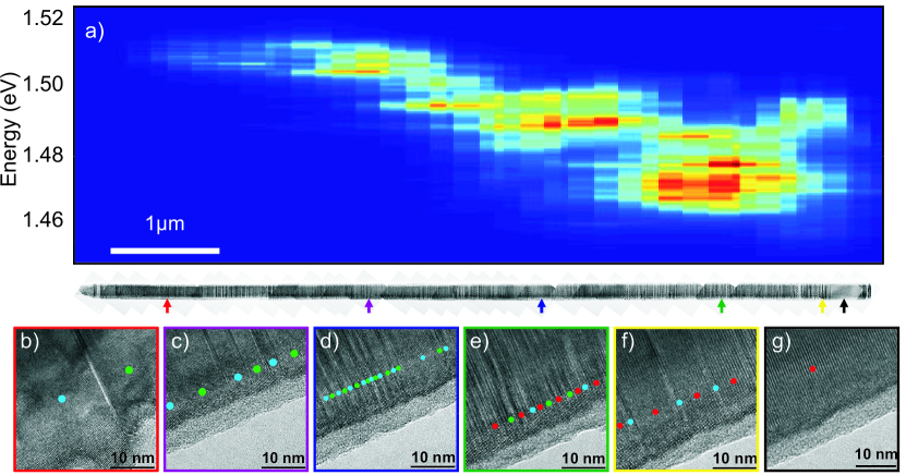
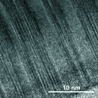
Fig. 7a shows the spatial dependence in a 7 m long nanowire with a diameter of 170 nm. Below the PL scan we have included TEM micrographs representative of various locations on the nanowire. From the structural point of view the nanowire is composed of two regions: (i) one with zinc-blende and a variation in twin density. (ii) one with a mixture of zinc-blende and wurtzite phases similar to a slightly disordered superlattice. The left side of the figure corresponds to the tip of the nanowire, which is in the zinc-blende phase with rotational twins separated by nm, shown in Fig. 7b. From left to right (towards the base of the nanowire), the density of deviations from an ideal zinc-blende crystal structure increases in a regular way.
Within 6 m from the left end of the nanowire these deviations are predominantly rotational twins and can be described considering a gradually increasing statistical twin density. For example, at positions 1 m, 3 m and 5 m, we observe a twin density of 60, 223 and 479 twins/m, respectively, shown in Fig. 7c-d. This increase in the twin density is accompanied by a regular red-shift of the PL peak from 1.50 to 1.48 eV. The PL signal is spatially discontinuous.
In the final third of the nanowire the concept of twin density is not sufficient to describe the structure of the nanowire, as segments of wurtzite phase appear regularly. We can describe considering the fraction of wurtzite phase present in the nanowire. At a distance of 6 m from the tip, the highly dense twin lattice turns into an alternation of 2 to 5 nm thick zinc-blende and wurtzite sections. At that point, the percentage of wurtzite is and the average spacing of each of the phases nm (Fig. 7e). Moving forward towards the right, the percentage of wurtzite quickly increases up to 100%, approximately 400 nm before the bottom of the nanowire. Some stacking faults and inclusions of zinc-blende smaller than 1 nm are observed right at the base, as shown in Fig. 7f. A continuous wurtzite region of 290 nm is also found, shown in Fig. 7g. This region is followed by a single 2.4 nm insertion of zinc-blende followed by 84 nm of wurtzite. Exactly at the base, we find a 46 nm thick section with a mixture of wurtzite and zinc-blende. The gradual decrease of wurtzite fraction and twins is related to the increase in As4 pressure during the growth Spirkoska et al. (2009).
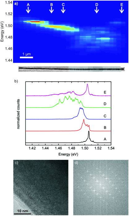
Interestingly, for the nanowire section where the twin density increases, the PL shifts from 1.51 down to 1.48 eV. After this, consistent with the regions where wurtzite sections appear clearly, the PL peak shifts further down to 1.46 eV. At the final section of the nanowire a blue-shift of the PL energy is observed. We never observe PL signal above 1.515 eV. A total of four nanowires were investigated with the direct correlation method. They all showed a similar behavior. Another example is shown in Fig. 8a.
The measurements presented above raise two main questions:
1) In the
top two thirds of the nanowire, why is the twinning density shifting
the PL emission towards lower energies from 1.51 to 1.48 eV?
2) Can
one derive the values of the conduction and valence band discontinuity
between wurtzite and zinc-blende from the correspondence between the
TEM and PL measurements?
In order to address the first question, we start by analyzing what seems to be a twin density dependence of the PL emission. Indeed, we have observed a significant red-shift (40 meV) for a twin density varying from 50 to 500 twins/m. Various causes may be responsible for this. For example, it is known that the binding energy of excitons confined in quantum well–like structures increases Miller et al. (1981). However in GaAs, even in the ideal 2D confinement limit, this could not account for a shift of more than 12 meV at most Miller et al. (1981). It is known that a change of effective mass within the quantum well plane could further increase the exciton binding energies Ropers et al. (2007). However the in-plane effective masses are not expected to change so significantly in wurtzite GaAs De and Pryor (2010). Most importantly, the presumably type II nature of the transition actually leads to a separation of electrons and holes thus diminishing the Coulomb interaction between the carriers. Moreover, a type II superlattice of single wurtzite layers in zinc-blende with varying superlattice periodicity cannot be an explanation because it would lead to a blue shift instead of a red shift. Finally, we must consider the possible correlation between the twin density and the appearance of single structures with several consecutive twins, corresponding to thin sections of the wurtzite phase. The occurrence of one twin is often illustrated as one monolayer of wurtzite. Multiple consecutive twinning leads to the formation of thicker wurtzite segments, which could account for the PL peaks below the GaAs band gap.
For a relatively homogeneous twin density over a length of several hundreds of nm, the twin density in that region gives directly the probability for a twinning event to occur during nucleation of a GaAs atomic layer in the (111) direction:
| (1) |
where is the cubic GaAs lattice constant and is the density of twins in the region of the nanowire. Assuming statistical independence of the twinning process Johansson et al. (2006) and the law of large numbers the probability of subsequent twinning events to occur is given by . We can therefore derive the average distance between such occasional segments consisting of consecutive twins.
| (2) |
In order to reveal the existence of multiple twinning and formation of thin segments of wurtzite, we examined each of the HRTEM micrographs along the nanowire. We found sections formed by monolayers (ML) of wurtzite in regions with increasing twin density. HRTEM micrographs corresponding to and are shown in Fig. 9a-b. The position of these sections corresponds to regions in the nanowire with high PL intensity. In Fig. 9c we plot the PL peak position as a function of the twin density of the nanowire section. Low temperature PL is very sensitive to the presence of such inhomogeneities with lower recombination energies. The majority of photogenerated carriers diffuse to the wurtzite quantum wells (lower energy) where they recombine. The line widths of the peaks are extremely sharp with a FWHM below 2.5 meV, which further corroborates our explanation (Fig. 8b). We also plot the position of the peaks observed in positions where twin stacks with n between 1 and 4 are observed by HRTEM. Clearly, the redshift in the PL peaks is correlated with the existence of consecutive twins and the existence of 1, 2 and 3 ML thick single wurtzite regions.
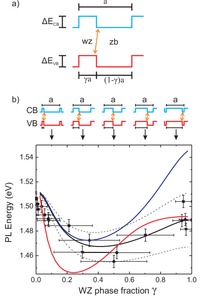
In the last third of the nanowire, segments of wurtzite appear regularly, as shown in Fig. 7e. In the PL mapping, multiple peaks are observed from 1.49 down to 1.455 eV. The final part on the right end of the nanowire is composed of pure wurtzite GaAs material segments with a length of up to 290 nm, see Fig. 7f-g, with small insertions of the zinc-blende structure. This region shows again PL emission above 1.49 eV. In order to address the question of whether the band offsets between wurtzite and zinc-blende GaAs phases can be determined, we plot the PL peaks as a function of the wurtzite phase fraction in Fig. 10. The horizontal error bars represent the microscopic variations of the actual nonperiodic heterostructure from an ideal homogeneous superlattice. Peaks at 1.455 eV correspond to regions of the nanowire exhibiting approximately 50:50 composition of the wurtzite and zinc-blende phases. Peaks at energies higher than 1.455 eV correspond to sections in the nanowire richer in one of the two phases. We point out that the highest energy PL peaks in the region with pure wurtzite correspond to a band gap of 1.504 eV; we never observed PL at energies above the free exciton of zinc-blende GaAs.
Finally, we propose a model to explain the PL emission in the last third of the nanowire. To this end, we calculate the miniband formation of a homogeneous superlattice (SL) with type II band alignment and band offsets and , shown in Fig. 10a, using a Kronig-Penney model. The overall lattice periodicity was set to nm which is the widest periodicity observed by TEM in the region of 50:50 phase composition, see Fig. 11. The largest periodicities in the structure correspond to the lowest recombination energies. Low temperature microphotoluminescence is most sensitive to the transitions with the lowest recombination energies. The calculations were performed for various valence and conduction band offsets and are plotted in Fig. 10b varying the relative thickness of the wurtzite and zinc-blende segments in the superlattice and considering the experimental band gap of zinc-blende GaAs in all cases. We want to note that the calculations are neglecting modifications of the band structure from strain Zardo et al. (2009) and spontaneous polarization of the hexagonal phase Bernardini et al. (1997). As a first attempt to provide a quantitative explanation, we use the values meV and meV obtained in earlier theoretical work Murayama and Nakayama (1994), and effective masses in wurtzite GaAs identical to the experimental ones for zinc-blende GaAs. The result is shown in Fig. 10b. Clearly, there is a disagreement between the theory and the experimental data for sections of the nanowire with a large wurtzite content. By least square fitting of the experimental data with the periodic superlattice model we can estimate meV and meV.
III.3 Calculation of the band offset and effective masses
| (eV) | (eV) | (meV) | (meV) | |
|---|---|---|---|---|
| DFT-LDA Murayama and Nakayama (1994) | 0.614 | 84 | 117 | |
| DFT-LDA Yeh et al. (1994) | 0.44 | - | - | |
| DFT-GW Zanolli et al. (2007) | 1.133 | - | - | |
| EP De and Pryor (2010) | 1.519111Based on fit to experimental zinc-blende band gap | 79.2 | 63.2 | |
| DFT-LDA | 0.351 | 114 | 70 | |
| DFT-HSE06 | 1.405 | 122 | 101 | |
| experiment | 1.51 |
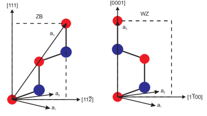
In order to obtain more accurate band offsets and effective mass values, we performed electronic structure calculations in the context of Density Functional Theory (DFT) Kohn and Sham (1965) using VASP Kresse and Furthmüller (1996). For the full band-structure throughout the Brillouin Zone (BZ), we employed the standard Local Density Approximation (LDA) Ceperley and Alder (1980); Perdew and Zunger (1981), with corresponding pseudopotentials. It is well known that this type of approach does not reproduce well the unoccupied part of the electronic spectrum and the energy band gap. Recently, it was shown that both the band gap Marsman et al. (2008) and the excitation energies Paier et al. (2008) are vastly improved by applying a screened Hartree–Fock hybrid exchange functional (HSE06) Heyd et al. (2003); Krukau et al. (2006). However, such calculations due to their high computational cost can be performed only for selected high-symmetry points in the BZ. Our approach then consists of performing a full band-structure calculation with the LDA method and using the HSE06 results to correct the excited states, by applying a uniform shift equal to the band gap correction for the zinc-blende structure; we are fully aware that such a “scissor operator” approach may not be adequate Remediakis and Kaxiras (1999), but for the bands of interest this approach gives very good results as explained below. For the hybrid exchange calculations we employed the PBE exchange-correlation functional in the DFT part Perdew et al. (1996) and PAW potentials to represent the ions Blöchl et al. (2003). We use a unit cell that has the same number of atoms in the zinc-blende and wurtzite lattices, by doubling one of the lattice vectors of the former, as shown in Fig. 12. We used plane-wave energy cutoffs of 326 eV for the LDA and 400 eV for the HSE06 calculations, and a reciprocal space Monkhorst-Pack grid of k-points Monkhorst and Pack (1976). We used the experimental in-plane lattice constant of zinc-blende (3.99 Å) corresponding to bulk Å. This is very close to the calculated ones, (3.95 Å) for both the zinc-blende and wurtzite phases. For this we neglected the effect of strain and influence of band structure.
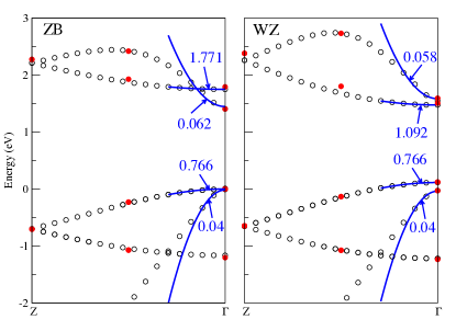
The results of the calculations are collected in Table 1 and the band structures for the zinc-blende and wurtzite phases are shown in Fig. 13, along the important directions, that is, [111] for zinc-blende and [0001] for wurtzite. We can calculate the band structure of this interface and assign each band to relevant wurtzite or zinc-blende phase, based on density distribution and similarity to bands of the bulk zinc-blende and wurtzite structure. In this way we can get information of band alignment/offsets of this interface. It is clear from the plot in Fig. 13 that along these directions in reciprocal space the uniform shift of excited LDA states (open black circles) by an amount equal to the band gap correction for the zinc-blende phase, brings them to excellent agreement with the calculated HSE06 results (filled red circles). The calculated band offsets are meV and meV, and effective masses along the [0001] wurtzite orientation are and ; the corresponding values for the [111] zinc-blende orientation are and . The essential difference is in the electron effective mass, which comes from the folding of the bands along the [0001] wurtzite orientation, as seen in Fig. 13. The corresponding superlattice model curve using the calculated band offsets and wurtzite effective masses is shown in Fig. 10b. Our first principles calculations indicate that the band gap of wurtzite GaAs is 21 meV lower compared to the band gap of the zinc-blende phase are in good agreement with the experimental data. Our experimentally determined band offsets are also in excellent agreement with band offsets recently calculated by De and Pryor De and Pryor (2010) using an Empirical Pseudopotential method (see Table 1).
IV Conclusions
In conclusion, we have presented results on a new technique that enables the experimental direct correlation between confocal micro-photoluminescence measurements and the structural characterization with high resolution transmission electron microscopy of nanowires consisting of nearly 100% wurtzite and presenting wurtzite/zinc-blende polytypism. The observations are in good agreement with theoretical predictions for the band gap and band offsets between the wurtzite and zinc-blende phases of GaAs. In wurtzite GaAs nanowires, we observe photoluminescence always below 1.52 eV. Taking into account the electronic confinement, the results indicate that the electronic band gap of wurtzite GaAs phase is slightly smaller than zinc-blende GaAs with an estimated .
The results on the polytypic nanowires are multiple. First, we correlate the appearance of wurtzite sections with the probability of twin formation. Then, we link the position of the luminescence with the stacking sequence of the wurtzite and zinc-blende phases. Due to the fact that the actual nanowire heterostructure is non periodic, an exact calculation for the optical transitions would require a model including the complete stacking sequence of each nanowire with atomic precision; it is extremely challenging to determine this sequence experimentally. Using a more simple periodic superlattice model, we have demonstrated that the experimental findings can be well explained despite the drastic simplifications of the model; we determine for the first time an experimental estimation for the band offsets of meV and meV. These band offsets correspond to a band gap for wurtzite GaAs of approx. 23 meV lower compared to the band gap of the zinc-blende phase. This is in excellent agreement with our results on pure wurtzite GaAs nanowires, other experiments Moewe et al. (2008), our first principles calculations and other recent band structure calculations De and Pryor (2010) . Furthermore, a slightly smaller band gap of the wurtzite phase of GaAs is supported by our general observation that even though both nanowire samples contain large amounts of wurtzite GaAs, we have never observed PL emission above the band gap of zinc-blende GaAs.
Acknowledgements.
The authors thank G. Abstreiter, T. Garma, D. Spirkoska and M. Bichler for their experimental support and discussions. We thank A. Petroutchik and L. T. Baczewski for the preparation of the Au-covered substrates for NW growth. This research was supported by Marie Curie Excellence Grant ’SENFED’, the DFG excellence cluster Nanosystems Initiative Munich, as well as SFB 631 and ERC Starting Grant ’Upcon’. This work was partially supported by the Spanish Government projects Consolider Ingenio 2010 CSD2009 00013 IMAGINE and CSD2009 00050 MULTICAT. J.A. acknowledge the funding from the Spanish CSIC project NEAMAN and MICINN project MAT2010-15138 (COPEON). The authors would like to thank the TEM facilities in the Interdisciplinary Center for Electron Microscopy in Lausanne and in Barcelona. E.R. acknowledge financial support from the ERA Nanoscience Project ’QOptInt’. E.R. and D.S. thank for support via SFB 689.References
- Cui and Lieber (2001) Y. Cui and C. M. Lieber, Science 291, 851 (2001).
- Samuelson et al. (2004) L. Samuelson, M. T. Björk, K. Deppert, M. Larsson, B. J. Ohlsson, N. Panev, A. I. Persson, N. Sköld, C. Thelander, and L. R. Wallenberg, Proceedings of the Eleventh International Conference on Modulated Semiconductor Structures, Physica E 21, 560 (2004).
- Cui et al. (2003) Y. Cui, Z. Zhong, D. Wang, W. U. Wang, and C. M. Lieber, Nano Letters 3, 149 (2003).
- Bjork et al. (2002) M. T. Bjork, B. J. Ohlsson, T. Sass, A. I. Persson, C. Thelander, M. H. Magnusson, K. Deppert, L. R. Wallenberg, and L. Samuelson, Applied Physics Letters 80, 1058 (2002).
- Wang et al. (2005) W. U. Wang, C. Chen, K.-h. Lin, Y. Fang, and C. M. Lieber, Proceedings of the National Academy of Sciences of the United States of America 102, 3208 (2005).
- Duan et al. (2001) X. Duan, Y. Huang, Y. Cui, J. Wang, and C. M. Lieber, Nature 409, 66 (2001).
- Chan et al. (2008) C. K. Chan, H. Peng, G. Liu, K. McIlwrath, X. F. Zhang, R. A. Huggins, and Y. Cui, Nat Nano 3, 31 (2008).
- Tian et al. (2007) B. Tian, X. Zheng, T. J. Kempa, Y. Fang, N. Yu, G. Yu, J. Huang, and C. M. Lieber, Nature 449, 885 (2007).
- Kayes et al. (2005) B. M. Kayes, H. A. Atwater, and N. S. Lewis, Journal of Applied Physics 97, 114302 (2005).
- Lauhon et al. (2002) L. J. Lauhon, M. S. Gudiksen, D. Wang, and C. M. Lieber, Nature 420, 57 (2002).
- Gudiksen et al. (2002) M. S. Gudiksen, L. J. Lauhon, J. Wang, D. C. Smith, and C. M. Lieber, Nature 415, 617 (2002).
- Fontcuberta i Morral et al. (2008) A. Fontcuberta i Morral, D. Spirkoska, J. Arbiol, M. Heigoldt, J. R. Morante, and G. Abstreiter, Small 4, 899 (2008).
- Heigoldt et al. (2009) M. Heigoldt, J. Arbiol, D. Spirkoska, J. M. Rebled, S. Conesa-Boj, G. Abstreiter, F. Peiro, J. R. Morante, and A. Fontcuberta i Morral, Journal of Materials Chemistry 19, 840 (2009).
- Heiß et al. (2009) M. Heiß, A. Gustafsson, S. Conesa-Boj, F. Peiro, J. R. Morante, G. Abstreiter, J. Arbiol, L. Samuelson, and A. Fontcuberta i Morral, Nanotechnology 20, 075603 (6pp) (2009).
- Ross (2009) F. M. Ross, Nat Nano 4, 17 (2009).
- Caroff et al. (2009) P. Caroff, K. A. Dick, J. Johansson, M. E. Messing, K. Deppert, and L. Samuelson, Nat Nano 4, 50 (2009).
- Algra et al. (2008) R. E. Algra, M. A. Verheijen, M. T. Borgstrom, L.-F. Feiner, G. Immink, W. J. P. van Enckevort, E. Vlieg, and E. P. A. M. Bakkers, Nature 456, 369 (2008).
- Park et al. (1994) C. H. Park, B.-H. Cheong, K.-H. Lee, and K. J. Chang, Phys. Rev. B 49, 4485 (1994).
- Strite and Morkoc (1992) S. Strite and H. Morkoc, Journal of Vacuum Science & Technology B: Microelectronics and Nanometer Structures 10, 1237 (1992).
- Davidson et al. (2007) F. M. Davidson, D. C. Lee, D. D. Fanfair, and B. A. Korgel, J. Phys. Chem. C 111, 2929 (2007).
- Murayama and Nakayama (1994) M. Murayama and T. Nakayama, Phys. Rev. B 49, 4710 (1994).
- Bao et al. (2008) J. Bao, D. C. Bell, F. Capasso, J. B. Wagner, T. Mårtensson, J. Trägårdh, and L. Samuelson, Nano Letters 8, 836 (2008).
- Pemasiri et al. (2009) K. Pemasiri, M. Montazeri, R. Gass, L. M. Smith, H. E. Jackson, J. Yarrison-Rice, S. Paiman, Q. Gao, H. H. Tan, C. Jagadish, X. Zhang, and J. Zou, Nano Letters 9, 648 (2009).
- Akopian et al. (2010) N. Akopian, G. Patriarche, L. Liu, J.-C. Harmand, and V. Zwiller, Nano Letters 10, 1198 (2010), pMID: 20205446, http://pubs.acs.org/doi/pdf/10.1021/nl903534n .
- Hoang et al. (2009) T. B. Hoang, A. F. Moses, H. L. Zhou, D. L. Dheeraj, B. O. Fimland, and H. Weman, Applied Physics Letters 94, 133105 (2009).
- Martelli et al. (2007) F. Martelli, M. Piccin, G. Bais, F. Jabeen, S. Ambrosini, S. Rubini, and A. Franciosi, Nanotechnology 18, 125603 (4pp) (2007).
- Moewe et al. (2008) M. Moewe, L. C. Chuang, S. Crankshaw, C. Chase, and C. Chang-Hasnain, Applied Physics Letters 93, 023116 (2008).
- Spirkoska et al. (2009) D. Spirkoska, J. Arbiol, A. Gustafsson, S. Conesa-Boj, F. Glas, I. Zardo, M. Heigoldt, M. H. Gass, A. L. Bleloch, S. Estrade, M. Kaniber, J. Rossler, F. Peiro, J. R. Morante, G. Abstreiter, L. Samuelson, and A. Fontcuberta i Morral, Phys. Rev. B 80, 245325 (2009).
- Ropers et al. (2007) C. Ropers, M. Wenderoth, L. Winking, T. C. G. Reusch, M. Erdmann, R. G. Ulbrich, M. Grochol, F. Grosse, R. Zimmermann, S. Malzer, and G. H. Döhler, Phys. Rev. B 75, 115317 (2007).
- Arbiol et al. (2009) J. Arbiol, S. Estrade, J. D. Prades, A. Cirera, F. Furtmayr, C. Stark, A. Laufer, M. Stutzmann, M. Eickhoff, M. H. Gass, A. L. Bleloch, F. Peiro, and J. R. Morante, Nanotechnology 20, 145704 (9pp) (2009).
- Lim et al. (2009) S. K. Lim, M. Brewster, F. Qian, Y. Li, C. M. Lieber, and S. Gradečak, Nano Letters 9, 3940 (2009).
- Wagner and Ellis (1964) R. S. Wagner and W. C. Ellis, Applied Physics Letters 4, 89 (1964).
- Rudolph et al. (2009) A. Rudolph, M. Soda, M. Kiessling, T. Wojtowicz, D. Schuh, W. Wegscheider, J. Zweck, C. Back, and E. Reiger, Nano Letters 9, 3860 (2009).
- De and Pryor (2010) A. De and C. E. Pryor, Phys. Rev. B 81, 155210 (2010).
- Birner et al. (2007) S. Birner, T. Zibold, T. Andlauer, T. Kubis, M. Sabathil, A. Trellakis, and P. Vogl, Electron Devices, IEEE Transactions on 54, 2137 (2007).
- Miller et al. (1981) R. C. Miller, D. A. Kleinman, W. T. Tsang, and A. C. Gossard, Phys. Rev. B 24, 1134 (1981).
- Johansson et al. (2006) J. Johansson, L. S. Karlsson, C. P. T. Svensson, T. Martensson, B. A. Wacaser, K. Deppert, L. Samuelson, and W. Seifert, Nat. Mater. 5, 574 (2006).
- Zardo et al. (2009) I. Zardo, S. Conesa-Boj, F. Peiro, J. R. Morante, J. Arbiol, E. Uccelli, G. Abstreiter, and A. Fontcuberta i Morral, Phys. Rev. B 80, 245324 (2009).
- Bernardini et al. (1997) F. Bernardini, V. Fiorentini, and D. Vanderbilt, Phys. Rev. B 56, R10024 (1997).
- Yeh et al. (1994) C.-Y. Yeh, S.-H. Wei, and A. Zunger, Phys. Rev. B 50, 2715 (1994).
- Zanolli et al. (2007) Z. Zanolli, F. Fuchs, J. Furthmüller, U. von Barth, and F. Bechstedt, Phys. Rev. B 75, 245121 (2007).
- Kohn and Sham (1965) W. Kohn and L. J. Sham, Phys. Rev. 140, A1133 (1965).
- Kresse and Furthmüller (1996) G. Kresse and J. Furthmüller, Phys. Rev. B 54, 11169 (1996).
- Ceperley and Alder (1980) D. M. Ceperley and B. J. Alder, Phys. Rev. Lett. 45, 566 (1980).
- Perdew and Zunger (1981) J. P. Perdew and A. Zunger, Phys. Rev. B 23, 5048 (1981).
- Marsman et al. (2008) M. Marsman, J. Paier, A. Stroppa, and G. Kresse, Journal of Physics: Condensed Matter 20, 064201 (2008).
- Paier et al. (2008) J. Paier, M. Marsman, and G. Kresse, Phys. Rev. B 78, 121201 (2008).
- Heyd et al. (2003) J. Heyd, G. E. Scuseria, and M. Ernzerhof, J. Chem. Phys. 118, 8207 (2003).
- Krukau et al. (2006) A. V. Krukau, O. A. Vydrov, A. F. Izmaylov, and G. E. Scuseria, J. Chem. Phys. 125, 224106 (2006).
- Remediakis and Kaxiras (1999) I. N. Remediakis and E. Kaxiras, Phys. Rev. B 59, 5536 (1999).
- Perdew et al. (1996) J. P. Perdew, K. Burke, and M. Ernzerhof, Phys. Rev. Lett. 77, 3865 (1996).
- Blöchl et al. (2003) P. Blöchl, C. Först, and J. Schimpl, Bulletin of Materials Science 26, 33 (2003).
- Monkhorst and Pack (1976) H. J. Monkhorst and J. D. Pack, Phys. Rev. B 13, 5188 (1976).